Defect healing at room temperature in pentacene thin films
and improved transistor performance
Abstract
We report on a healing of defects at room temperature in the organic semiconductor pentacene. This peculiar effect is a direct consequence of the weak intermolecular interaction which is characteristic of organic semiconductors. Pentacene thin-film transistors were fabricated and characterized by in situ gated four-terminal measurements. Under high vacuum conditions (base pressure of order 10-8 mbar), the device performance is found to improve with time. The effective field-effect mobility increases by as much as a factor of two and mobilities up to 0.45 cm2/Vs were achieved. In addition, the contact resistance decreases by more than an order of magnitude and there is a significant reduction in current hysteresis. Oxygen/nitrogen exposure and annealing experiments show the improvement of the electronic parameters to be driven by a thermally promoted process and not by chemical doping. In order to extract the spectral density of trap states from the transistor characteristics, we have implemented a powerful scheme which allows for a calculation of the trap densities with high accuracy in a straightforward fashion. We show the performance improvement to be due to a reduction in the density of shallow traps eV from the valence band edge, while the energetically deeper traps are essentially unaffected. This work contributes to an understanding of the shallow traps in organic semiconductors and identifies structural point defects within the grains of the polycrystalline thin films as a major cause.
pacs:
73.61.Ph, 73.20.At, 73.61.-rI Introduction
Organic electronics now rapidly enters the consumer markets. Field-effect mobilities in polycrystalline organic semiconductors are comparable to the mobilities in hydrogenated amorphous silicon and the organic semiconductors can be deposited by thermal evaporation or from solution at low costs on large areas. Pentacene and its soluble derivatives are among the most promising organic semiconductors for organic thin-film transistor applications.Lin et al. (1997); Sheraw et al. (2003)
Organic semiconductors are distinct in that they generally consist of neutral molecules which interact by rather weak forces (predominantly Van der Waals forces). The energy associated with a Van der Waals bond is 10-3-10-2 eV, i.e. orders of magnitude smaller than the energy of a covalent bond (several eV).Silinsh and Capek (1994) Therefore, organic semiconductors are soft, have a low mechanic strength and a high compressibility, low melting and sublimation temperatures and a large thermal expansion coefficient. The weak interaction forces between the molecules not only enable low-cost processing but also lead to peculiarities such as the existence of at least four different pentacene polymorphs or an even negative thermal expansion coefficient.Mattheus et al. (2001); Haas et al.
As in the case of amorphous inorganic materials, the charge transport in organic semiconductors can be described with a mobility edge or transport level concept. In the case of crystalline small molecule organic semiconductors such as pentacene, the mobility edge may be identified with the valence or conduction band edge and the charge carriers are transported in extended states. However, the charge carriers are transported in states above a mobility edge and are multiply trapped by and thermally released from trap states below the mobility edge. Consequently, the conduction of charge in organic semiconductors and thus the transistor characteristics critically depend on trap states. Energetically deep traps influence the subthreshold swing of a device which needs to be sufficiently steep for a low power operation. The density of shallow traps, on the contrary, can dominate the effective field-effect mobility. Trap states in organic semiconductors have long been a subject of investigation.Probst and Karl (1975) This topic is currently attracting much attention due to the crucial importance of trap states for the emerging applications of organic field-effect transistors.Northrup and Chabinyc (2003); Jurchescu et al. (2004); Kang et al. (2005); Goldmann et al. (2006); Kalb et al. (2007); Krellner et al. (2007) The shallow traps in particular are poorly understood.
The density of trap states as a function of energy can be derived from the transistor characteristics. On the one hand, a density of states function can be postulated a priori and the corresponding transistor characteristic can be simulated by means of a suitable computer program. The density of states function is then iteratively refined until, after a number of predictor-corrector loops, good agreement between the measured characteristic and the simulated curve is achieved.Völkel et al. (2002); Scheinert et al. (2002); Oberhoff et al. (2007) On the other hand, the density of states function can be calculated from the linear regime transfer characteristics in a straightforward fashion. A number of such extraction schemes has been suggested.Horowitz et al. (1995); Schauer (1999); Lang et al. (2004); De Angelis et al. (2006a) This approach has the advantage of giving an unambiguous result but, depending on the complexity of the extraction scheme, spurious errors may result from simplifying assumptions.
Organic thin-film transistors (TFTs) are most often characterized after the samples have been exposed to ambient air and in situ electrical characterization is very rare.Kiguchi et al. (2005); Knipp et al. (2007) The organic semiconductors, however, are generally presumed to be sensitive to water vapor and oxygen. Moreover, the transistors are often characterized by two-terminal measurements which do not allow to distinguish between contact effects and effects of the semiconducting layer. The gated four-terminal method yields the field-effect conductivity and the effective field-effect mobility free from contact effects. It also allows for an extraction of the device contact resistance.Takeya et al. (2003); Goldmann et al. (2004); Pesavento et al. (2004, 2006)
For this work pentacene served as a prototypical small molecule semiconductor and we have investigated the performance of pentacene thin-film transistors by in situ gated four-terminal measurements. The corresponding trap states functions were derived with a straightforward extraction scheme which had been successfully used to understand trap states in hydrogenated amorphous silicon.
II Experimental
II.1 Device fabrication
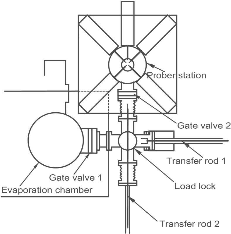
Pentacene from Aldrich (purum) was sublimation purified twice and was introduced into the evaporation chamber soon after the purification. As substrates we used heavily doped Si wafers with a 260 nm thick SiO2 layer. The substrates were cleaned with hot acetone and hot isopropanol (MOS grade) in an ultrasonic bath. Immediately after the cleaning, the substrates were mounted on a sample holder and were introduced into the in situ device fabrication and characterization system via the load lock (Fig. 1). The evaporation chamber and the prober station were both separated from the load lock with a gate valve and were constantly kept under vacuum (base pressure mbar). The vacuum in the evaporation chamber and in the prober station was maintained with a cryopump and a turbopump, respectively. The substrates were introduced into the evaporation chamber with transfer rod 1 and were placed on a shadow mask for the pentacene evaporation. A high precision mask positioning mechanism allowed for a proper adjustment of the mask with respect to the substrates.
The substrates were kept in high vacuum for approximately 24 h prior to the device fabrication. After that time, also the pressure in the turbo-pumped load lock was mbar. A 50 nm thick film of pentacene was evaporated through the shadow mask onto the Si/SiO2 substrates while the substrates were kept at room temperature. After the pentacene evaporation, the sample holder was positioned on a shadow mask for the gold evaporation with transfer rod 1 and the pentacene TFTs were completed by evaporating 40 nm thick gold electrodes.
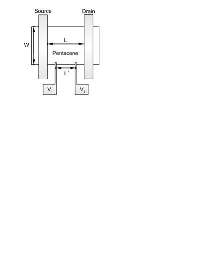
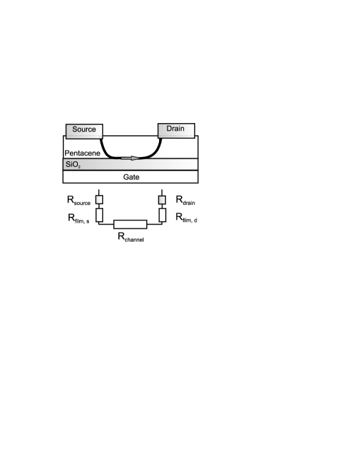
The resulting transistor test structures are shown schematically in Fig. 2. The transistors consisted of a well-defined stripe of pentacene and had voltage sensing electrodes with little overlap to the pentacene film. It has been shown that the use of a “masked” pentacene film and a proper alignment of the electrodes is important for the four-terminal measurement.Pesavento et al. (2006) The channel length and width of the devices was m and m, respectively. The voltage sensing electrodes were situated at and , such that the distance between these electrodes was m.
After the completion of the device fabrication, the samples were transported to the prober station by means of transfer rod 1 and transfer rod 2 (Fig. 1).
II.2 Electrical characterization
For the electrical measurements we used a HP 4155A semiconductor parameter analyzer connected to five microprobers at the prober station. Transfer characteristics in the linear regime were measured in steps of 0.2 V (drain voltage V). In all cases, the forward and the reverse sweeps were measured. The integration time was 20 ms and the delay time was 0 s. In addition to the drain current , the voltage drops and between the grounded source and the two voltage sensing electrodes were measured at each gate voltage (gated four-terminal measurement). All electrical measurements were carried out in the dark.
A device was measured initially h after the completion of the pentacene evaporation. Subsequently, the same device was measured regularly (normally twice a day) for approximately one week while being kept in the prober station at mbar in the dark.
In some experiments, the effect of oxygen or nitrogen exposure on the device characteristics was investigated. This was done by introducing a continuous flow of gas (pureness Vol.-) into the prober station through a leak valve, thus adjusting the partial pressure of the gas within the prober station. A few days prior to the device fabrication for the gas exposure experiments, the prober station was filled with the respective gas through the leak valve in order to flush the gas supply line and the valve. The prober station was then re-evacuated and the supply lines were held at an overpressure of atm until the leak valve was opened in the experiment.
In other experiments, the influence of annealing was explored by means of an electrical heating element on the sample holder tray in the prober station.
III Parameter extraction
In this section, we elucidate the extraction of key parameters from the device characteristics. Linear regime transfer characteristics are particularly interesting for the study of semiconductor physics, because the gradual channel approximation is valid which leads to a drastic simplification of the device physics. The two-dimensional problem is approximated by two one-dimensional equations, i.e. Possion’s equation for the charge distribution perpendicular to the insulator-semiconductor interface and a simple ohmic current-voltage relationship.
III.1 Basic parameter extraction
In single crystalline inorganic MOSFETs above a threshold voltage, essentially all the trap states are filled and the charge which is induced by the gate appears in the valence/conduction band.Shur and Hack (1984) Both the constant mobility in the above threshold regime and the threshold voltage are important device parameters. This approach may also be valid in the case of organic single crystal transistors, i.e. organic field-effect transistors with a very low trap density. However, contact effects often severely affect the characteristics of these devices because of the low channel resistance.Podzorov et al. (2003)
As in the case of amorphous silicon field-effect transistors, the equations developed for single crystalline MOSFETs are not suitable to describe organic TFTs due to the increased trap density.Shur and Hack (1984); Horowitz et al. (1999, 2004) Depending on the density of trap states, the majority of charge carriers induced by the gate may be trapped even at relatively high gate voltages.Oberhoff et al. (2007) Provided that contact effects are negligible, the drain current of an organic TFT in the linear regime is given by
| (1) |
is the field-effect conductivity which is the effective field-effect mobility multiplied with the total gate induced charge per unit area , i.e
| (2) |
is the flatband voltage and the capacitance per unit area. The effective field-effect mobility is one of the most important device parameters and, for a p-type semiconductor such as pentacene, can be written as
| (3) |
where and are respectively the density of free and trapped holes per unit area. is the extended state mobility. The effective field-effect mobility is expected to increase with gate voltage even at relatively high gate voltages, because the ratio increases as the valence band is bent towards the Fermi energy.Horowitz et al. (1999)
The flatband voltage is the gate voltage which needs to be applied in order to enforce flat bands at the insulator-semiconductor interface. A non-zero flatband voltage can result from a difference of the semiconductor and the gate Fermi levels. More importantly, the flatband voltage is influenced by charge that is permanently trapped at the interface or within the gate dielectric and only the latter contribution can explain the large shifts of the transfer characteristics that are sometimes observed in experiments.Wang et al. (2006) The flatband voltage is approximately equal to the onset voltage of the device. The onset voltage is defined as the gate voltage, where the drain current, as a function of gate voltage, rises sharply if plotted on a logarithmic scale. In the present work we assume that the flatband voltage is equal to the onset voltage.
From a technological point of view it is useful to define a threshold voltage which marks the transition between the regime below threshold to the regime above threshold. In the above-threshold regime, the deep traps are filled and the field-effect mobility is less strongly dependent on gate voltage. The above-threshold regime in an organic TFT can be understood as being in between the below-threshold regime and the above-threshold regime of a single crystalline MOSFET.Shur and Hack (1984) It can be shown that the field-effect mobility in the above-threshold regime follows a power law and this allows for a refined extraction of the field-effect mobility and the threshold voltage .Shur and Hack (1984); Horowitz et al. (2000, 2004)
In this study we do, however, follow the IEEE Standard for the characterization of organic transistors and materials. The field-effect conductivity can be calculated from
| (4) |
With Eq. 2 and Eq. 4 can be approximated as
| (5) |
Since this approach is frequently used it has the advantage that the values of can easily be compared. Moreover, the definition and extraction of a threshold voltage is not necessary. However, small errors in the absolute value of the field-effect mobility and its gate voltage dependence are to be expected since the derivation rests on the assumption of a weak dependence of the field-effect mobility on gate voltage.Horowitz et al. (2004)
In an organic field-effect transistor, a significant fraction of the drain voltage may drop at the contacts which can introduce significant errors when extracting the field-effect conductivity and the field-effect mobility. From gated-four terminal measurements, the conductivity can be derived without error with . is the distance between the voltage sensing electrodes and the voltage drop between these electrodes (Fig. 2). The contact-corrected field-effect conductivity is then given by
| (6) |
The effective field-effect mobility is not influenced by contact effects when calculated from
| (7) |
In the following we use the expressions “two-terminal conductivity” and “two-terminal mobility” as short hand for Eq. 4 and Eq. 5. We furthermore use the abbreviations “four-terminal conductivity” and “four-terminal mobility” for the quantities defined in Eq. 6 and Eq. 7.
The device contact resistance was extracted from the four-terminal measurement and was compared to the device channel resistance . We now assume a linear voltage drop all along the channel, i.e. from the source to the drain. With this assumption, the voltage drop across the transistor channel is and the voltage drop at the contacts is . The contact resistance is thus given by
| (8) |
and the channel resistance by
| (9) |
III.2 Advanced parameter extraction
The gate voltage dependence of the field-effect mobility reflects the spectral density of trap states close to the valence band. A number of direct extraction schemes has been suggested to obtain the underlying density of states function.Horowitz et al. (1995); Schauer (1999); Lang et al. (2004); De Angelis et al. (2006a) In these approaches, the relevant energy scale is derived from the activation energy of the current (i.e. the field-effect conductivity) which is obtained from temperature dependent measurements. If, however, the electrical characteristics of a transistor change on a timescale comparable to the time of a temperature dependent measurement (hours), this approach is not suitable.
Grünewald et al. have suggested an extraction scheme of high accuracy for amorphous silicon thin-film transistors which allows to convert a single linear regime transfer characteristic into the underlying density of states function.Grünewald et al. (1980, 1981); Weber et al. (1982) It is based on surprisingly few simplifying assumptions including:
-
a)
the gradual channel approximation,
-
b)
the semiconductor is homogenous normal to the dielectric-semiconductor interface, and
-
c)
insulator surface states only introduce an initial band bending without applied field, i.e. contribute to a non-zero flatband voltage .
Extraction schemes often rest on the abrupt approximation: all the charge is assumed to reside in a region close to the dielectric-semiconductor interface of depth . Grünewald’s method, however, is not based on this simplification but takes proper account of the gate-induced band bending. In the following, the key equations of the extraction scheme are given.
Within the Boltzmann approximation, the field-effect conductivity is given by
| (10) |
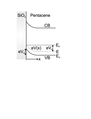
Now is the gate voltage above the flatband voltage, is the thickness of the pentacene film, is the band shift as a function of the distance from the insulator-semiconductor interface and is the conductivity at flatband. can be approximated as
| (11) |
is an effective density of extended states and the energy of the valence band edge far from the insulator-semiconductor interface. The situation is depicted in Fig. 3. The complicated dependence of the band shift on the space coordinate in Eq. 10 can be eliminated and an equation can be derived, which implicitly contains the interface potential as a function of gate voltage:
| (12) |
is the thickness of the gate insulator and and are the dielectric constants of the insulator and the semiconductor, respectively (see Ref. Grünewald et al., 1980 for a derivation of this equation). For each gate voltage, Eq. III.2 can be evaluated numerically and a value for the interface potential is obtained. Eventually, we have the complete function .
In most general terms, the total hole density (volume density) is
| (13) |
where N(E) is the density of states function. The total hole density can be calculated as
| (14) |
i.e. by a numerical differentiation of the previously obtained set of data .Grünewald et al. (1981) Differentiating Eq. 13 with respect to the band shift yields
| (15) |
Several deconvolution methods exist to solve this type of equation for , e.g. with cubic spline functions.Schauer et al. (1986); Krellner et al. (2007) However, for a slowly varying density of states function (absence of monoenergetic states), the difference between and is expected to be relatively small on a logarithmic scale.Schauer et al. (1986) Consequently, we obtain the final result by a numerical derivation of with respect to the interface potential according to
| (16) |
Within this zero temperature approximation, the band shift at the interface is equal to the energy of the respective traps relative to the Fermi energy of the sample, i.e. (Fig. 3).
We have used Grünewald’s method to interpret the current voltage characteristics from pentacene TFTs. We used the “four-terminal conductivity” as a starting point which allows to extract a density of states function free from contact artifacts. A simple MATLAB® coding allowed for the calculation of the density of states function from Eq. III.2, 14 and 16.
IV Results
IV.1 Improvement of the device performance with time
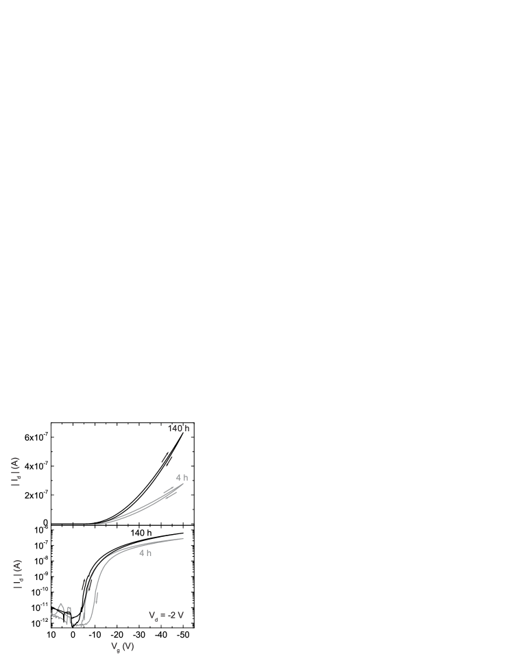
Fig. 4 shows the transfer characteristic from a pentacene TFT measured 4 h and 140 h after the completion of the pentacene evaporation. The device was kept at mbar all along. After 140 h, the device shows an increased on-current. In addition, the current hysteresis is reduced: at a current level of A, the difference between the forward and the reverse sweep is 3.8 V after 4 h and 1.2 V after 140 h. The subthreshold swing is essentially unaffected by the high vacuum storage. There is a small shift of the onset voltage to more positive voltages from -6.4 V after 4 h to -4.9 V after 140 h.
An increase in on-current can be due to changes of the pentacene film and/or to a reduction of the device contact resistance. The gated four-terminal method can disentangle the field-effect conductivity and the device contact resistance. In Fig. 5 we show the “four-terminal conductivity” after 4 h and after 140 h, as derived from the forward sweeps (Eq. 6). The “two-terminal conductivity” (Eq. 4) is shown for comparison. The “four-terminal conductivity” is increased after 140 h, which reveals changes of the pentacene film. The difference between the “four-terminal conductivity” and the “two-terminal conductivity” is reduced after 140 h, indicative of an additional contact resistance reduction.

Fig. 6 shows the “four-terminal mobility” derived with Eq. 7 and the “two-terminal mobility” calculated from Eq. 5. As expected, the mobility increases monotonically with gate voltage. When comparing both measurements, a significant improvement in mobility can be ascertained. At V, the mobility is cm2/Vs after 4 h and cm2/Vs after 140 h, i.e. has increased by a factor of 2.111We compare mobilities for comparable total charge densities. Since we only observe small onset voltage shifts, a correction of the gate voltage by the onset voltage is not necessary.

In Fig. 7 we show the width-normalized contact resistance according to Eq. 8 and, for comparison, the width-normalized channel resistance (Eq. 9). There is a drastic reduction in contact resistance. At V the contact resistance decreases by a factor of from cm to cm. The channel resistance decreases by a factor of . The channel resistance is always higher than the contact resistance: at V and after 4 h the channel resistance is times larger than the contact resistance and after 140 h it is times the contact resistance. Thus, the device is always dominated by the channel resistance.

IV.2 Influence on the density of states function
In Sec. IV.4 and IV.5 we show, that the performance improvement is not due to doping by a residual gas but due to a healing of defects at room temperature. To investigate the energetic position of these defects, we have applied the scheme described in Sec. III.2. The first step was to calculate the interface potential as a function of gate voltage with Eq. III.2. We have assumed a dielectric constant of for SiO2 and for pentacene. Fig. 8(a) shows the result of the extraction for the measurement after 4 h and after 140 h. In a second step, the density of states was calculated by two numerical differentiations of according to Eq. 14 and Eq. 16. Some degree of data smoothing was applied in order to obtain a reasonably smooth density of states function. Fig. 8(b) shows the final result for the measurement after 4 h and after 140 h. A step width of 0.2 V in the gate voltage sweeps leads to a good resolution of the deep states.
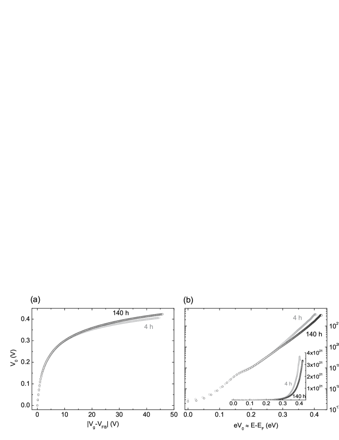
The Fermi energy of the sample coincides with the zero point of the energy scale in Fig. 8(b). At high gate voltages, the valence band edge at the interface is close to the Fermi level. Consequently, the Fermi level is approximately eV from the valence band edge at flatband. For comparison, the bandgap of pentacene is 2.24-2.5 eV.Gundlach et al. (2006) The interface potential in Fig. 8(a) reflects the spectral density of trap states. At low gate voltages bands bend easily, which indicates a low trap density. At high gate voltages, however, band bending is more difficult and this is indicative of a high trap density very close to the valence band edge.
The energetics in Fig. 8(a) are in good agreement with activation energies from temperature dependent measurements of pentacene-based transistors.Vissenberg and Matters (1998); Lang et al. (2004); De Angelis et al. (2006b) In these studies the activation energy is derived from by means of Arrhenius plots. Assuming the abrupt approximation, Eq. 10 can be approximated as
| (17) | |||||
and we have . The activation energy from the Arrhenius plots is approximately equal to the energetic difference between the Fermi level and the valence band at the interface. The activation energy is found to be eV near the onset voltage of the devices and eV when the devices are turned on completely. shows a similar functional dependence on gate voltage as in Fig. 8(a).Vissenberg and Matters (1998); Lang et al. (2004); De Angelis et al. (2006b)
From Fig. 8(b) it is clear that it is the shallow traps with energies approximately eV from the valence band edge which are reduced by the high vacuum storage. It is the density of these states that influences the value of the field-effect mobility . A relatively small reduction leads to a significant improvement in field-effect mobility. The traps which are deeper in energy are essentially unaffected, resulting in an almost identical subthreshold swing of the transfer characteristics.
Both after 4 h and after 140 h, the density of states function can reasonably well be approximated by a single exponential function
| (18) |
It is however slightly steeper than exponential. Fitting the curves in Fig. 8(b) for eV to Eq. 18 yields the parameters meV for the measurement after 4 h and meV for the measurement after 140 h. This is in good agreement with results for pentacene TFTs obtained with a device simulation program.Oberhoff et al. (2007); Pernstich et al. In Ref. Oberhoff et al., 2007, characteristic slopes of meV and 37 meV are specified and in Ref. Pernstich et al., a slope of meV was determined.
IV.3 Comparison of several experiments
The effects described above, i.e. a significant increase in the “four-terminal mobility”, a drastic reduction in the contact resistance and a reduction in the current hysteresis, have been observed in all experiments. Fig. 9 shows the evolution of the “four-terminal mobility” and the contact resistance with time for four different runs. The values are for and are normalized by the value obtained after h.222The value for the contact resistance was taken at . For the mobility, an average in the range V to V was taken since in some cases the derivative of the drain current was more noisy. A time span of at least 4 h was allowed in between subsequent measurements. The absolute values for the mobility and the contact resistance from the initial measurement are summarized in Table 1.
| Run | [cm2/Vs] | [cm] | [V] |
| 1 | 0.22 | 1.95 | -6.4 |
| 2 | 0.24 | 1.10 | -4.1 |
| 3 | 0.14 | 3.03 | -5.1 |
| 4 | 0.14 | 3.35 | -6.4 |
| Oxygen | 0.12 | 3.98 | -6.2 |
| Nitrogen | 0.10 | 4.70 | -7.0 |
| Annealing | 0.10 | 4.55 | -5.7 |
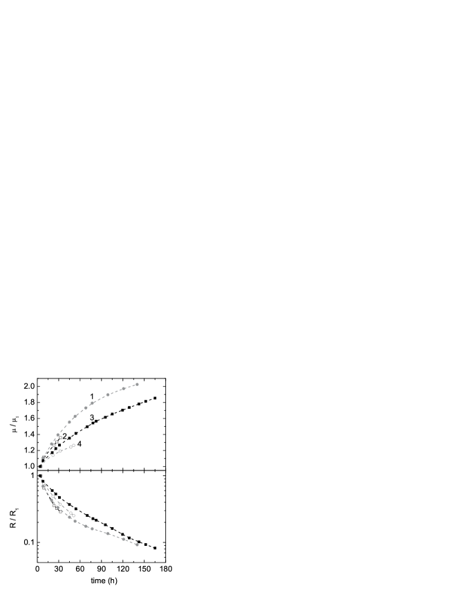
Table 1 also contains the respective onset voltages. Initially, the onset voltage is between V and V and shifts in all cases by less than 2.5 V during the course of an experiment. The reduction of the current hysteresis takes place in the early stages of the experiments. In all four runs, the current hysteresis is significantly reduced after the first h to V at a current level of A. Subsequently, there is only a small further reduction of the current hysteresis.
We now proceed by providing experimental evidence that the performance improvement is not due to doping of the pentacene thin films by residual oxygen or nitrogen and show that the performance improvement is a thermally promoted process.
IV.4 Influence of oxygen and nitrogen
Even at a pressure of order mbar the time for the formation of a monolayer of residual gas molecules is less than ten minutes.Roth (1990) In the case of semiconducting polymers experimental evidence indicates that doping leads to an increased field-effect mobility.Brown et al. (1997) This may be understood if one assumes the charge transport to take place by variable-range hopping and the doping to increase the density of states/hopping sites.Brown et al. (1997) In crystalline small molecule organic semiconductors, however, charge transport in extended states has to be considered. Doping raises the Fermi level of the sample. This results in an increase of the (flatband) conductivity, since the density of free holes is increased (Eq. 11). When the device is turned on, however, the current flow is due to the gate induced holes and the holes from a chemical doping are negligible in Eq. 3. Thus it would not immediately be obvious how chemical doping would increase the field-effect mobility in pentacene.
Both oxygen and nitrogen have been reported to have the capability of doping pentacene. Gas exposure is found to lead to a shift of the transistor transfer characteristic to more positive voltages which corresponds to a shift of the Fermi level.Ogawa et al. (2005); Knipp et al. (2007) In other studies, an increase in conductivity of gas exposed pentacene thin-films or single crystals was observed in two-terminal measurements without gate-field induced charge. The increased conductivity is ascribed to an increased charge carrier density caused by doping.Kuroda and Flood (1961); Jurchescu et al. (2005); Parisse et al. (2006) There seems to be no evidence that doping leads to an increased effective mobility in pentacene. Recent measurements on rubrene single crystals also show doping not to increase the field-effect mobility.So et al. (2007)
The issue of reversibility and the importance of light for the doping is not completely clear. Doping is observed when pentacene thin films are exposed to relatively high partial pressures (0.01 atm-1 atm) of oxygen or nitrogen in the presence of light.Kuroda and Flood (1961); Ogawa et al. (2005); Parisse et al. (2006) The doping effect by oxygen is reported to be negligible in the absence of light.Kuroda and Flood (1961); Ogawa et al. (2005) Ultraviolet photoelectron spectroscopy (UPS) before and after exposure to mbar oxygen could not detect a lasting effect on the position of the energy levels.Vollmer et al. (2005) According to Ref. Knipp et al., 2007, exposing pentacene TFTs to an oxygen partial pressure of mbar leads to a doping of the films.
While the mobility increase in crystalline/polycrystalline samples cannot be easily linked to chemical doping, a reduction of the contact resistance might be reconciled with doping. From inorganic semiconductor physics it is well known that doping close to a contact reduces the contact resistance. Moreover, it has been shown with UPS that oxygen, at a low partial pressure, can lead to a lowering of the injection barrier for holes at an Au/pentacene interface.Vollmer et al. (2005)
The results of our studies concerning the effect of gas exposure on the field-effect mobility and on the contact resistance are discussed in the following. If e.g. oxygen was responsible for the increase in mobility and/or reduction in contact resistance, an increase in the oxygen partial pressure should accelerate the rate of the respective process. Fig. 10 shows the influence of oxygen on the “four-terminal mobility” and on the contact resistance (see Table. 1 for the initial parameters). After 41 h, the oxygen partial pressure was raised from a total turbo-pumped background pressure of order mbar to mbar. After 69 h, the partial pressure was increased to mbar and eventually, after 98 h, the chamber was re-evacuated. The increase in oxygen partial pressure does not accelerate the gradual increase in mobility or the reduction in contact resistance. The dashed red line in Fig. 10 is an estimate for the time-dependence of the contact resistance if the sample had not been exposed to oxygen. Consequently, the increase in oxygen partial pressure even leads to a delay of the reduction in contact resistance. It is noteworthy that neither the small current hysteresis nor the subthreshold swing of the devices are effected by the oxygen exposure. Since oxygen at a partial pressure of mbar for 28 h and at a partial pressure of mbar for 29 h appears not to accelerate the development of the device parameters with time one would conclude that oxygen at the base pressure is not responsible for the performance improvement.
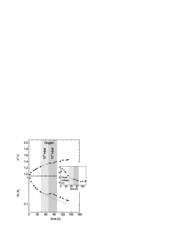
The inset in Fig. 10 shows the onset voltage for each of the measurements. The overall shift of the onset voltage is small and smooth ( V over h). In particular, there is no sudden shift of the transfer characteristic after an increase in oxygen partial pressure. Therefore, there is no evidence that oxygen at partial pressures mbar leads to a doping of the films.
Fig. 11 shows the analogous experiment with nitrogen. After 50 h the nitrogen partial pressure was increased to mbar, followed by an increase to mbar after 69.5 h. After 98 h, the system was pumped down to the base pressure of order mbar. The increase in nitrogen partial pressure does not accelerate the increase in mobility or the reduction in contact resistance. Similarly to the oxygen experiment we have estimated the time-dependence of the contact resistance if the sample had not been exposed to nitrogen (dashed red line in Fig. 11). Clearly, the nitrogen exposure leads to a slowing down of the decrease in contact resistance. The nitrogen exposure leaves the small current hysteresis and the subthreshold swing unaffected. Residual nitrogen is not responsible for the performance improvement.
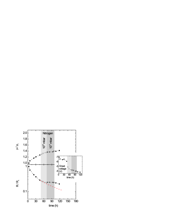
The inset in Fig. 11 shows the device onset voltage as a function of time. When the nitrogen partial pressure is increased to mbar there is a sudden shift of the onset voltage to more positive voltages by 1.2 V. We take this as evidence for doping by nitrogen at a partial pressure of mbar. When the pressure is increased to mbar, there is no additional marked shift of the onset voltage.
IV.5 Annealing at slightly elevated temperatures
Annealing pentacene thin films at moderate temperatures (e.g. 50∘ C) results in an improved crystallinity of the films as seen by XRD.Komoda et al. (2002); Ye et al. (2003); Kang et al. (2004) When concentrating on the channel region adjacent to the gate dielectric in a field-effect transistor, the annealing is found to leave the mobility unchanged (Ref. Komoda et al., 2002) or to lead to an increased mobility (Ref. Kang et al., 2004). Since the interaction between the pentacene molecules is of the weak Van der Waals type, it is not too surprising that annealing at moderate temperatures leads to an improved crystallinity of the films. Moreover, it seems plausible that structural defects can be “annealed” even at room temperature, which will account for the effects we observe. In this scenario we would expect an acceleration of the performance improvement at higher temperatures. Fig. 12 shows the influence of such an annealing at 320 K (see Table 1 for the initial parameters). After 44.5 h, the sample temperature was slowly raised from RT to 320 K at a rate of ∘/min. Transfer characteristics were measured after the temperature of 320 K had been reached. After 104.5 h, the heating was switched off, followed by a slow cooling of the sample to room temperature. Two effects can be discerned in the annealing process. First, the overall level of the mobility and the contact resistance are affected by the increase in temperature since both quantities depend on temperature. Second, and more significant in the present context, is the rate of change: after raising the temperature, the increase in mobility and the decrease in contact resistance is accelerated significantly. This is indicated by the dashed red lines in Fig. 12.
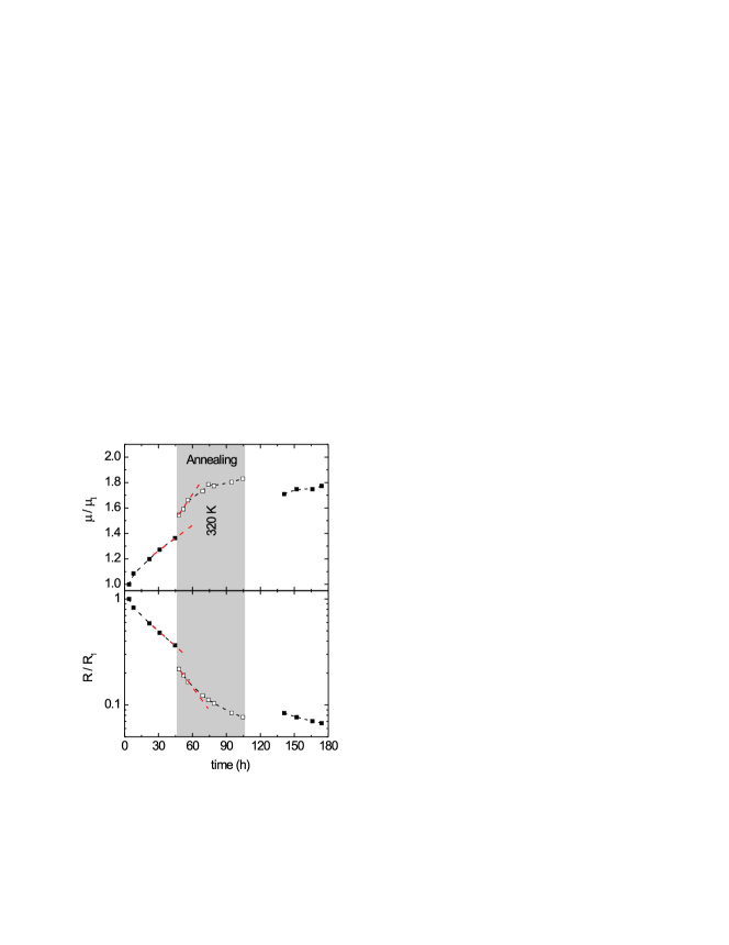
In an additional experiment (not shown), the sample temperature was raised from room temperature to 310 K after 45.5 h and was increased to 320 K after 74 h. Even at 310 K, which is not much above room temperature (), the increase in mobility and the decrease in contact resistance is accelerated noticeably.
All these results taken together clearly indicate an improvement of the electronic parameters driven by a thermally promoted process, and not by chemical doping. We suggest this process to be a healing of structural defects. We now discuss the microscopic origin of the relevant traps and suggest how a reduced trap density can lead to a reduced contact resistance.
V Discussion
V.1 Defect healing at room temperature
Pentacene thin-films on Si/SiO2 substrates are known to have a layered structure and the layers are parallel to the substrate. Within these layers, the molecules are arranged in a herringbone pattern and are oriented almost perpendicular with respect to the substrate. It has been shown by high impedance STM that some of the pentacene molecules in the layers are displaced along their long molecular axis, while the two-dimensional packing is not disturbed.Kang et al. (2005) With electronic structural calculations it could be shown that the displaced molecules result in traps eV from the valence band edge.Kang et al. (2005)
In Sec. IV.2 we have shown that only the shallow traps eV from the valence band edge are reduced during the high vacuum storage at room temperature. We suggest that a major cause of the shallow traps in pentacene thin films are pentacene molecules within the grains that are slightly misplaced, i.e. various types of structural point defects. Some of these defects are in a metastable state before relaxation. They require only a small amount of energy in order to align which can be provided by the thermal energy at room temperature. This is a direct manifestation of the weak intermolecular interaction which is characteristic of small molecule organic semiconductors. The “annealing” of shallow traps at room temperature can easily explain the increase in the effective field-effect mobility.
V.2 Defects and contact resistance
In a simplistic view, the contact resistance is given by the energetic difference between the work function of the metal and the ionization energy of the pentacene. In reality, however, a clear correlation between the metal work function and the contact resistance is often not observed.Gundlach et al. (2006) Interface states can significantly affect the energetics at the metal-pentacene interface.Pesavento et al. (2004) In a top contact device, also the film resistance should contribute to the contact resistance. The film resistance in pentacene devices with gold top contacts has even been suggested to dominate the contact resistance.Pesavento et al. (2006) The situation is illustrated in Fig. 13: the hole injection at the source/pentacene interface is good, but the holes must cross the pentacene film in order to reach the channel at the insulator-semiconductor interface. The intrinsic mobility perpendicular to the molecular layers is lower than parallel to the layers. Combined with high trap densities, this can result in a large resistance between the gold electrodes and the transistor channel. If the contact resistance is dominated by the film resistance, a reduction in the density of hole traps is therefore expected to lead to a reduced contact resistance.
VI Summary and conclusions
Pentacene thin-film transistors were made by thermal evaporation, employing a high precision in situ mask alignment mechanism. The devices were characterized electrically by gated four-terminal measurements without breaking the high vacuum (base pressure of order 10-8 mbar). Under the high vacuum conditions, the device performance is found to improve with time. Within approximately one week, the contact-corrected field-effect mobility improves by a factor of up to two and the device contact resistance typically decreases by more than an order of magnitude. In addition, the current hysteresis reduces significantly. We have shown that an increased partial pressure of oxygen or nitrogen does not accelerate the performance improvement. On the contrary, the gas exposure delays the decrease in contact resistance. Nitrogen was found to dope pentacene thin films at partial pressures as low as 10-6 mbar. Annealing at a slightly elevated temperature (e.g. 320 K), on the contrary, leads to an acceleration of the performance improvement.
Some defects within the pentacene “anneal” even at room temperature. This is a peculiarity of the physics of organic semiconductors, which is governed by the weak Van der Waals type interaction between the molecules. We have derived the spectral density of trap states from the “four-terminal conductivity”. The calculations show shallow traps eV from the valence band edge to be significantly affected by the defect healing. We suggest these traps to originate from structural point defects, i.e. slightly misaligned molecules within the grains of the polycrystalline film. The effective field-effect mobility critically depends on the number of these shallow traps and a relatively small reduction results in a significant improvement of the mobility. The contact resistance is likely to be dominated by the film resistance and also depends on the active traps within the film.
The method to calculate the spectral density of traps is a powerful tool to further elucidate the origin of trap states in organic semiconductors, provided that contact effects are properly taken into account. It is particularly suitable to study metastable defects in organic semiconductors, because the density of states function can be derived from a single transfer characteristic in an unambiguous fashion and with a minimal set of simplifying assumptions.
Acknowledgements.
The authors thank K. P. Pernstich, D. J. Gundlach and S. Haas for their help with the experimental setup and for valuable discussions.References
- Lin et al. (1997) Y. Y. Lin, D. J. Gundlach, S. F. Nelson, and T. N. Jackson, IEEE Electron Device Lett. 18, 606 (1997).
- Sheraw et al. (2003) C. D. Sheraw, T. N. Jackson, D. L. Eaton, and J. E. Anthony, Adv. Mater. 15, 2009 (2003).
- Silinsh and Capek (1994) E. A. Silinsh and V. Capek, Organic molecular crystals (AIP Press, New York, 1994).
- Mattheus et al. (2001) C. C. Mattheus, A. B. Dros, J. Baas, A. Meetsma, J. L. de Boer, and T. T. M. Palstra, Acta Crystallogr., Sect. C: Cryst. Struct. Commun. 57, 939 (2001).
- (5) S. Haas, B. Batlogg, C. Besnard, M. Schiltz, C. Kloc, and T. Siegrist, accepted for publication in Phys. Rev. B.
- Probst and Karl (1975) K. H. Probst and N. Karl, Phys. Status Solidi A 27, 499 (1975).
- Northrup and Chabinyc (2003) J. E. Northrup and M. L. Chabinyc, Phys. Rev. B 68, 041202(R) (2003).
- Jurchescu et al. (2004) O. D. Jurchescu, J. Baas, and T. T. M. Palstra, Appl. Phys. Lett. 84, 3061 (2004).
- Kang et al. (2005) J. H. Kang, D. da Silva, J. L. Bredas, and X. Y. Zhu, Appl. Phys. Lett. 86, 152115 (2005).
- Goldmann et al. (2006) C. Goldmann, D. J. Gundlach, and B. Batlogg, Appl. Phys. Lett. 88, 063501 (2006).
- Krellner et al. (2007) C. Krellner, S. Haas, C. Goldmann, K. P. Pernstich, D. J. Gundlach, and B. Batlogg, Phys. Rev. B 75, 245115 (2007).
- Kalb et al. (2007) W. L. Kalb, T. Mathis, S. Haas, A. F. Stassen, and B. Batlogg, Appl. Phys. Lett. 90, 092104 (2007).
- Völkel et al. (2002) A. R. Völkel, R. A. Street, and D. Knipp, Phys. Rev. B 66, 195336 (2002).
- Scheinert et al. (2002) S. Scheinert, G. Paasch, M. Schrödner, H. K. Roth, S. Sensfuss, and T. Doll, J. Appl. Phys. 92, 330 (2002).
- Oberhoff et al. (2007) D. Oberhoff, K. P. Pernstich, D. J. Gundlach, and B. Batlogg, IEEE Trans. Electron Devices 54, 17 (2007).
- Horowitz et al. (1995) G. Horowitz, R. Hajlaoui, and P. Delannoy, J. Phys. III France 5, 355 (1995).
- Schauer (1999) F. Schauer, J. Appl. Phys. 86, 524 (1999).
- Lang et al. (2004) D. V. Lang, X. Chi, T. Siegrist, A. M. Sergent, and A. P. Ramirez, Phys. Rev. Lett. 93, 086802 (2004).
- De Angelis et al. (2006a) F. De Angelis, S. Cipolloni, L. Mariucci, and G. Fortunato, Appl. Phys. Lett. 88, 193508 (2006a).
- Knipp et al. (2007) D. Knipp, A. Benor, V. Wagner, and T. Muck, J. Appl. Phys. 101, 044504 (2007).
- Kiguchi et al. (2005) M. Kiguchi, M. Nakayama, T. Shimada, and K. Saiki, Phys. Rev. B 71, 035332 (2005).
- Takeya et al. (2003) J. Takeya, C. Goldmann, S. Haas, K. P. Pernstich, B. Ketterer, and B. Batlogg, J. Appl. Phys. 94, 5800 (2003).
- Goldmann et al. (2004) C. Goldmann, S. Haas, C. Krellner, K. P. Pernstich, D. J. Gundlach, and B. Batlogg, J. Appl. Phys. 96, 2080 (2004).
- Pesavento et al. (2004) P. V. Pesavento, R. J. Chesterfield, C. R. Newman, and C. D. Frisbie, J. Appl. Phys. 96, 7312 (2004).
- Pesavento et al. (2006) P. V. Pesavento, K. P. Puntambekar, C. D. Frisbie, J. C. McKeen, and P. P. Ruden, J. Appl. Phys. 99, 094504 (2006).
- Shur and Hack (1984) M. Shur and M. Hack, J. Appl. Phys. 55, 3831 (1984).
- Podzorov et al. (2003) V. Podzorov, S. E. Sysoev, E. Loginova, V. M. Pudalov, and M. E. Gershenson, Appl. Phys. Lett. 83, 3504 (2003).
- Horowitz et al. (1999) G. Horowitz, R. Hajlaoui, D. Fichou, and A. El Kassmi, J. Appl. Phys. 85, 3202 (1999).
- Horowitz et al. (2004) G. Horowitz, P. Lang, M. Mottaghi, and H. Aubin, Adv. Funct. Mater. 14, 1069 (2004).
- Wang et al. (2006) A. Wang, I. Kymissis, V. Bulovic, and A. I. Akinwande, Appl. Phys. Lett. 89, 112109 (2006).
- Horowitz et al. (2000) G. Horowitz, M. E. Hajlaoui, and R. Hajlaoui, J. Appl. Phys. 87, 4456 (2000).
- Grünewald et al. (1980) M. Grünewald, P. Thomas, and D. Würtz, Phys. Status Solidi B 100, K139 (1980).
- Grünewald et al. (1981) M. Grünewald, K. Weber, W. Fuhs, and P. Thomas, J. Phys. 42, 523 (1981).
- Weber et al. (1982) K. Weber, M. Grünewald, W. Fuhs, and P. Thomas, Phys. Status Solidi B 110, 133 (1982).
- Schauer et al. (1986) F. Schauer, S. Nespurek, and O. Zmeskal, J. Phys. C 19, 7231 (1986).
- Gundlach et al. (2006) D. J. Gundlach, L. Zhou, J. A. Nichols, T. N. Jackson, P. V. Necliudov, and M. S. Shur, J. Appl. Phys. 100, 024509 (2006).
- Vissenberg and Matters (1998) M. C. J. M. Vissenberg and M. Matters, Phys. Rev. B 57, 12964 (1998).
- De Angelis et al. (2006b) F. De Angelis, L. Mariucci, S. Cipolloni, and G. Fortunato, J. Non-Cryst. Solids 352, 1765 (2006b).
- (39) K. P. Pernstich, B. Rössner, and B. Batlogg, submitted.
- Roth (1990) A. Roth, Vacuum Technology (Elsevier Science B. V., Amsterdam, 1990).
- Brown et al. (1997) A. R. Brown, C. P. Jarrett, D. M. de Leeuw, and M. Matters, Synth. Metal. 88, 37 (1997).
- Ogawa et al. (2005) S. Ogawa, T. Naijo, Y. Kimura, H. Ishii, and M. Niwano, Appl. Phys. Lett. 86, 252104 (2005).
- Kuroda and Flood (1961) H. Kuroda and E. A. Flood, Can. J. Chem. 39, 1981 (1961).
- Jurchescu et al. (2005) O. D. Jurchescu, J. Baas, and T. T. M. Palstra, Appl. Phys. Lett. 87, 052102 (2005).
- Parisse et al. (2006) P. Parisse, M. Passacantando, S. Picozzi, and L. Ottaviano, Org. Electron. 7, 403 (2006).
- So et al. (2007) W.-Y. So, J. M. Wikberg, D. V. Lang, O. Mitrofanov, C. L. Kloc, T. Siegrist, A. M. Sergent, and A. P. Ramirez, Solid State Commun. 142, 483 (2007).
- Vollmer et al. (2005) A. Vollmer, O. D. Jurchescu, I. Arfaoui, I. Salzmann, T. T. M. Palstra, P. Rudolf, J. Niemax, J. Pflaum, J. P. Rabe, and N. Koch, Eur. Phys. J. E 17, 339 (2005).
- Komoda et al. (2002) T. Komoda, Y. Endo, K. Kyuno, and A. Toriumi, Jpn. J. Appl. Phys. 41, 2767 (2002).
- Ye et al. (2003) R. B. Ye, M. Baba, K. Suzuki, Y. Ohishi, and K. Mori, Jpn. J. Appl. Phys. 42, 4473 (2003).
- Kang et al. (2004) S. J. Kang, M. Noh, D. S. Park, H. J. Kim, C. N. Whang, and C. H. Chang, J. Appl. Phys. 95, 2293 (2004).