e-mail ritz@pi1.physik.uni-stuttgart.de, Phone +49-(0)711-68564893, Fax +49-(0)711-68564886
7 February 2008
Influence of electronic correlations on the frequency-dependent hopping transport in Si:P
Abstract
\abstcolAt low energy scales charge transport in the insulating Si:P is dominated by activated hopping between the localized donor electron states. Thus, theoretical models for a disordered system with electron-electron interaction are appropriate to interpret the electric conductivity spectra. With a newly developed technique we have measured the complex broadband microwave conductivity of Si:P from 100 MHz to 5 GHz in a broad range of phosphorus concentration from 0.56 to 0.95 relative to the critical value cm-3 corresponding to the metal-insulator transition driven by doping.At our base temperature of = 1.1 K the samples are in the zero-phonon regime where they show a super-linear frequency dependence of the conductivity indicating the influence of the Coulomb gap in the density of the impurity states. At higher doping , an abrupt drop in the conductivity power law is observed. The dielectric function increases upon doping fol-lowing a power law in (). Dynamic response at elevated temperatures has also been investigated.
pacs:
numbers: 71.30.+h, 72.15.Rn, 72.20.Ee, 72.80.Ng1 Introduction
In a material of such an industrial importance like Si:P there are
still questions open about the low-energy excitations from the
ground state. In particular, the influence of electron-electron
interactions on the hopping transport and the critical behavior at
the metal-insulator transition (MIT) have attracted much attention
since decades. Though theoretical predictions on the
0 frequency-dependent response of an interacting
disordered system have already existed since many years [1],
experimental data still remain scarce and results obtained by
different groups and in different parameter ranges lack
consistency. Especially in the microwave range, from tens of MHz
till tens of GHz, with wavelengths from a few millimeters to a few
meters, no better means than the reso-nator techniques have been
used for a long time to study the broadband dynamic conductivity
of doped semiconductors. With a novel and advanced method of
measuring the broadband (100 MHz to 5 GHz) complex microwave
conductivity of that material class, we focus on the conductivity
power law in Si:P at 0 and at elevated
temperatures in a broad range of
donor concentration close to the MIT.
At concentrations of phosphorus in silicon below the critical
value of cm-3, the donor electron
states are strongly localized due to disorder in Anderson sense
[2] and the corresponding wave functions resemble
those of a hydrogen atom [3]. Since some degree of
compensation by impurities of the opposite type is considered
inevitable, charge transport at low excitation energies is by
variable-range hopping between the donor sites, randomly
distributed in space [3, 4].
1.1 Dynamic conductivity
The static conductivity
of the insulating Si:P vanishes
when . The main issue we address is that of power
laws of the frequency-dependent conductivity in the variable-range
hopping regi- me at zero temperature:
| (1) |
The theory of resonant photon absorption by pairs of states, one
of which is occupied by an electron and the other one is empty,
yields distinct limiting results for the conducti-
vity power law
in cases, where one of the relevant energy scales of the problem
dominates
over the others:
For the non-interacting system, where the photon ener- gy prevails over the electronic correlations, Mott has predicted a sub-quadratic frequency-dependence of the conductivity [4]:
| (2) | |||||
Here, is a numerical coefficient [1, 4], is the state density at the Fermi level, is the localization radius, is the most probable hopping distance and is the pre-exponen-tial factor of the overlap integral between the localized electron states.
Taking into account the Coulomb repulsion if both states in a pair would be occupied by an electron, Shklovskii and Efros corrected the picture of the energy levels before and after a photon is absorbed and derived to be a sub-linear function of frequency, as long as the Coulomb interaction term dominates over the photon energy [1]:
| (3) | |||||
At higher frequencies, in the opposite limit, the sub-quadratic
behavior known from Mott (2) is recovered.
The formula (3) is derived under the assumption of an
effectively constant density of states near the Fermi level.
This implies another characteristic energy of the system, the
Coulomb gap , to be small compared to and thus of no
significant effect on the states participating in the hopping
transport. The parabolic Coulomb gap forms in the density of the
impurity states around the Fermi level as another consequence of
the electronic correlations [3]. For the conductivity of
interacting electrons where the Coulomb term dominates over
the photon energy but falls inside the Coulomb gap, the reduction
of the density of states leads to a stronger, slightly
super-linear power law [1]:
| (4) |
1.2 Dielectric function
It is an additional advantage of a phase sensitive measurement to
gain the dielectric function from the imaginary part of the
complex conductivi-
ty [5]:
| (5) |
We denote by the full complex dielectric function of Si:P, relative to the permittivity of vacuum, and use the SI units throughout this text. As the MIT is approached upon doping , the localization radius diverges according to a power law [3]:
As a consequence, the electronic contribution to the dielectric function is also expected to diverge following a power law when the MIT is approached [6]:
| (6) |
where is the dielectric constant of
the
host material Si.
2 Experiments
2.1 Samples
Si:P-samples for this study were cut from a Czochralski-grown cylindrical crystal [7], nominally uncompensated, with a phosphorus concentration gradient along its axis. To remove distorted surface layers [8, 9], the samples were chemically and mechanically treated by well established procedures. The donor concentration was determined from the room-temperature resistivity [10] employing a commercial four-probe measurement system (FPP 5000 by Veeco Instruments). For high doping levels the resistivity ratio K)/K) (determined from standard dc measurements) is consistent with Ref. [11]. In the present work, measurements on Si:P-samples with relative donor concentration ranging from 0.56 to 0.90 relative to the critical value at the MIT are discussed, as summarized in Tab. 1.
| K) | ||||
|---|---|---|---|---|
| ( cm | ( cm) | |||
| 1.97 | 0.56 | 0.0162 | 1.13 | 23 |
| 2.29 | 0.65 | 0.0149 | 1.16 | 24.5 |
| 2.57 | 0.73 | 0.0139 | 1.10 | 28 |
| 2.91 | 0.83 | 0.0130 | 1.08 | 34 |
| 3.04 | 0.87 | 0.0127 | 1.05 | 41 |
| 3.14 | 0.90 | 0.0124 | 1.04 | 46 |
2.2 Broadband microwave spectroscopy
The broadband microwave spectrometer, previously employed for measuring metallic samples [13, 14], has been upgraded [12] with microwave components, calibration technique and evaluation procedure suitable to study the hopping transport in doped semiconductors at temperature as low as possible.
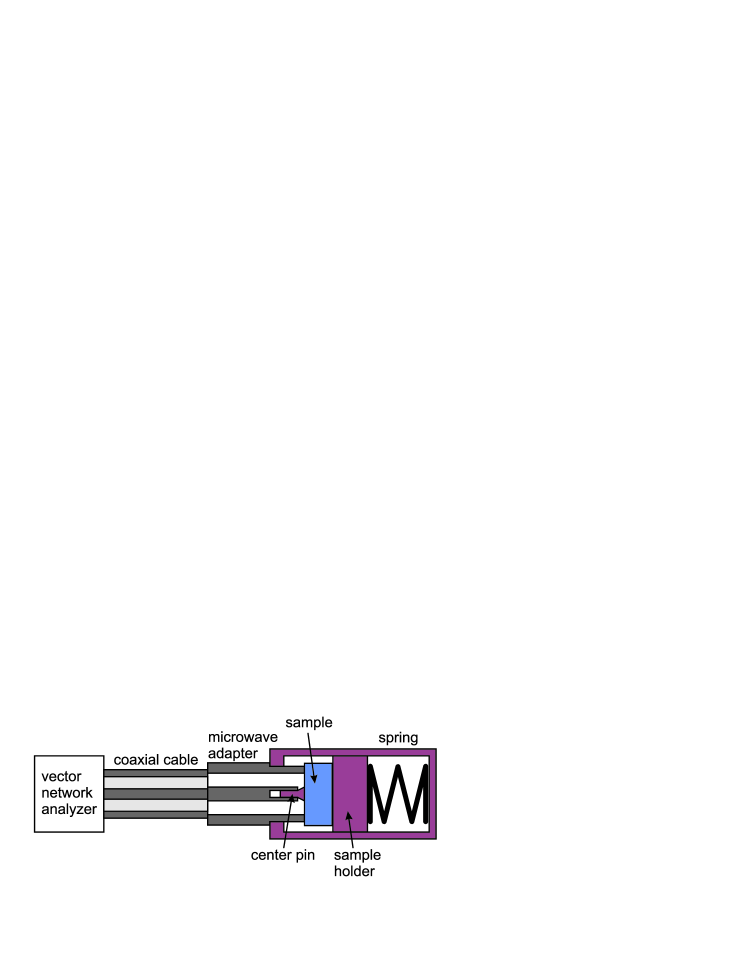
The sample with a flat surface terminates the 1.2m-long coaxial line, Fig.1, needed to transport the microwave signal from the source to the bottom of a 4He-pumped cryostat. The reflected signal, containing all the useful information about the sample, returns the same way back to the test set of a HP 8510 vector network analyzer. The measurement is phase sensitive and yields the complex reflection coefficient. After an extensive calibration procedure requiring three independent low temperature measurements of calibration samples under reproduced conditions, the reflection coefficient at the sample surface is obtained. The complex impedance is directly related to it via [15]:
| (7) |
with the characteristic impedance of the microwave line.
In a next step, the complex conductivity has to be extracted from the impedance . If material is insulating, there exists no direct solution, because the simple concepts known from metallic samples [14] fail here. In the case of an insulator, the surface impedance approach [5], useful for thick metallic samples, yields a wrong (i.e. too strong) frequency dependence of the conductivity . If the semiconducting sample is treated as a thin highly-conducting film, the conductivity values are suspiciously large [16].
2.3 Advanced data analysis
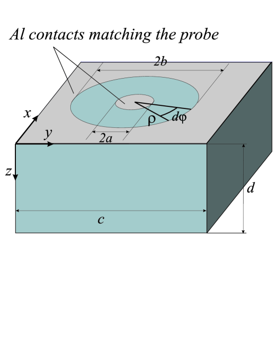
For these reasons, we have developed a general and rigorous solution for the problem. The electromagnetic wave penetrates deep into a thick insulating sample, Fig.2, and forms a three-dimensional distribution quite different from that of a plane wave. Thus, we work with a solution for the field distribution in an integral equation formulation, combined with the variational principle [17]. Ascertaining, that the electromagnetic field strength decreases below 1% at the depth corresponding to our sample thickness of 2 mm in the frequency range evaluated, we forbear from taking into account the secondary reflections at the back side of the sample as in the full-wave analysis at higher frequencies considered by Brom and collaborators [18]. The resulting formula connects the complex sample impedance to the wave vector , the latter containing the complex dielectric function we search for. (Note, that we hold to the convention for the Fourier-transformed of the electromagnetic field in accordance with [5, 17]. The opposite sign convention is used in Ref. [18, 19] and by the network analyzer.)
| (8) |
To solve this integral equation for we make use of the practical ideas from [19]. In a series expansion of the exponential function the terms higher than the third term are negligible below 5 GHz, integrating the rest one obtains a quadratic equation in [12]:
| (9) |
with the geometrical integrals mm and
mm3 numerically evaluated for the dimensions and of our
coaxial probe as shown in Fig.2.
2.4 Low-temperature ac measurements
The frequency range from 100 MHz to 5 GHz for the reflection coefficient measurements according to section 2.2 contains 300 frequency points: 200 equidistant points from 0.1 GHz to 1 GHz and 100 from 1 GHz to 5 GHz. The spectra are taken at the base temperature 1.1 K of our 4He-pumped cryostat as well as at elevated temperatures using a temperature controller Lake Shore 340 in an automatized procedure while heating the setup up to room temperature. All the reported samples prove to be in the zero-phonon regime at K because they show a saturation of and in the whole frequency range as K.

3 Results and discussion
For each doping concentration four to ten independent measurements have been conducted. From the best spectra (lowest noise and smallest influence of standing waves) mean values of the conductivity power and the dielectric constant have been determined.
3.1 Frequency dependence of the conductivity in the zero-phonon regime
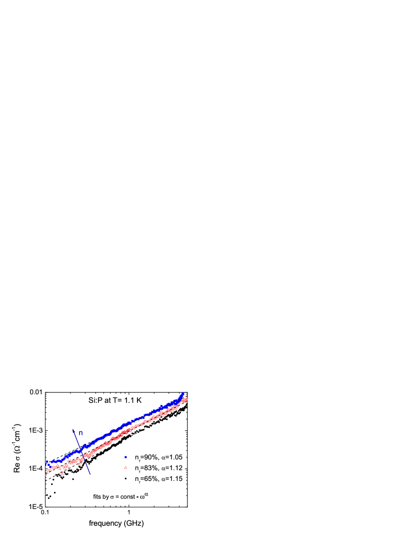
In Fig.3 the measured real part of the frequency-dependent conductivity is plotted on a log-log scale to identify the power law. The fits by a two-parameter function crossing the origin are shown by the dashed lines. In Fig.4 the mean values of the power are plotted against the relative dopant concentration. The frequency dependence of the conductivity clearly follows a super-linear power law in the whole doping range, where the exponent decreases slightly with doping; this effect becomes even stronger when is increased further. From this we infer, that hopping transport takes place deep inside the Coulomb gap corresponding to equation (4). A super-linear conductivity power law was previously observed in Si:As and Si:P by Castner and collaborators [20, 21] using resonator techniques at certain frequency within the range of the present work. Our results are in accord with the measurements on similar samples at higher frequencies (30 GHz to 3 THz) using optical techniques [22, 23]. In contrast, a sub-linear frequency dependence in the zero-phonon regime has been reported by Lee and Stutzmann [16] based on experiments on Si:B in the microwave range and by Helgren et al. [9] using quasi-optical experiments.
3.2 Temperature dependence of the conductivity
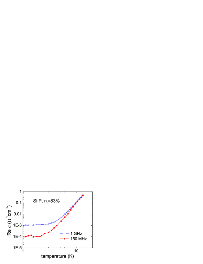
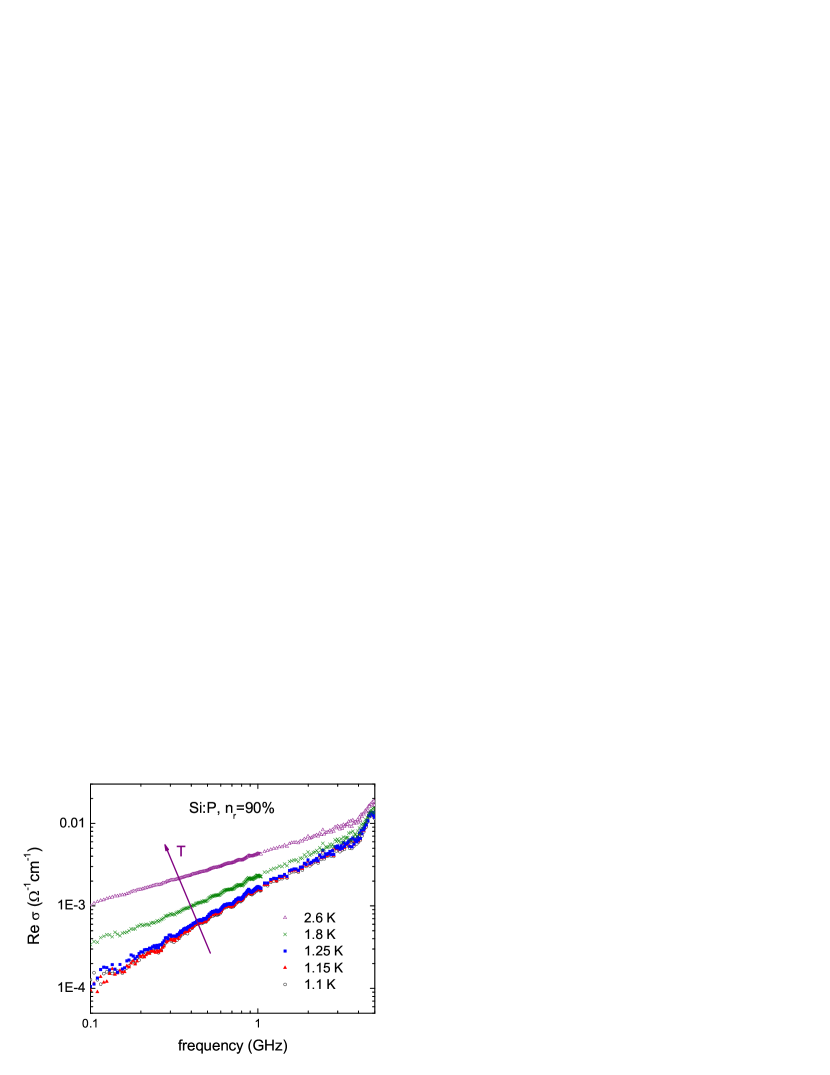
Leaving the zero-phonon regime by raising temperature, a gradual increase of the conductivity is observed for all investigated Si:P-samples. First, the temperature dependence is approximately linear in agreement with the prediction of Austin and Mott [1, 24]. With increasing , it gradually becomes stronger until the charge carrier activation into the conduction band dominates over the hopping transport. The onset of the thermal effects depends on the phosphorus concentration: the higher the doping, the lower the temperature at which the temperature dependence sets in. But the way it happens is the same for all the samples measured. Taking the example of , we have plotted the conductivity values in Fig.5 at fixed frequencies of 150 MHz and 1 GHz. Above K the curves merge into the thermally activated curve.
In fig. 6 the frequency dependent conductivity is plotted for different temperatures, for the example of the crystal with the high concentration ; the conductivity power law gradually decreases with rising temperature. The transition to a sub-linear power law upon raising is in accord with previous observations [21, 24, 25]; to our knowledge, the theoretical description of the gradual decrease of is lacking.
3.3 Dielectric function
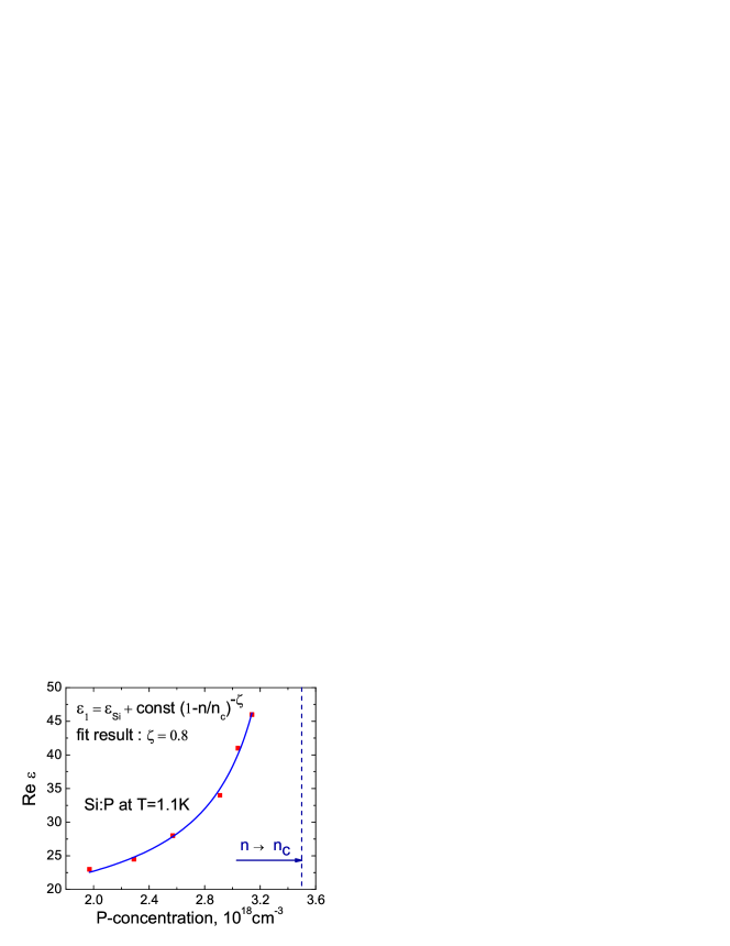
The dielectric function is independent of frequency in our frequency range, taking the measurement uncertainty into account. A fit with the function (6) results in an exponent 0.8, as shown in Fig.7.
4 Conclusion
Si:P-samples with relative doping from 56% to 90% show temperature-independent dynamic response at the temperature of 1.1 K. Over a wide frequency range (100 MHz to 5 GHz) the conductivity power law is slightly super-linear, with a faint decrease of the power upon doping. At higher doping, above 90 %, the conductivity power law drops abruptly. Interpretation and further studies at lower base temperature using 3He are in progress. At elevated temperatures the conductivity values are increasing and the power is falling gradually with rising . The electronic contribution to the dielectric function is constant and increases with phosphorus concentration as expected when the MIT is approached.
We thank A. L. Efros, H. v. Löhneysen and K. Holczer for
helpful discussions, A. W. Anajoh and M. Scheffler for the dc-measurements and die Landesgraduiertenför-
derung
Baden-Württemberg for the scolarship.
References
- [1] B. I. Shklovskii and A. L. Efros, Zh. Eksp. Teor. Fiz. 81, 406 (1981) [Sov. Phys. JETP 54, 218 (1981)]
- [2] P. W. Anderson, Phys. Rev. 109, 1492 (1958)
- [3] B. I. Shklovskii and A. L. Efros, Electronic Properties of Doped Semiconductors (Springer, Berlin, 1984),
- [4] N. F. Mott and E. A. Davis, Electronic Processes in Non-Crystalline Materials, 2nd edition (Clarendon Press, Oxford, 1979),
- [5] M. Dressel and G. Grüner, Electrodynamics of Solids (Cambridge University Press, Cambridge, 2002)
- [6] A. L. Efros and B. I. Shklovskii, phys. stat. sol. (b) 76, 475 (1976)
- [7] Single crystal grown by Société Générale Métallurgique de Hoboken and provided by D. Schweitzer.
- [8] Y. Ootuka, F. Komori, Y. Monden, S. Kobayashi, and W. Sasaki, Solid State Commun. 36, 827 (1980)
- [9] E. Helgren, N. P. Armitage, and G. Grüner, Phys. Rev. B 69, 014201 (2004)
- [10] W. R. Thurber, R. L. Mattis, Y. M. Liu, and J. J. Filliben, J. Elechtrochem. Soc. 127, 1807 (1980)
- [11] M. Hornung, Diploma thesis, Karlsruhe (1993)
- [12] E. Ritz and M. Dressel, to be published
- [13] M. Scheffler and M. Dressel, Rev. Sci. Instrum. 76, 074702 (2005)
- [14] J. C. Booth, Dong Ho Wu, and S. M. Anlage, Rev. Sci. Instrum. 65, 2082 (1994)
- [15] D. M. Pozar, Microwave Engineering (John Wiley & Sons, New York, 1998)
- [16] M. Lee and M. L. Stutzmann, Phys. Rev. Lett. 87, 056402 (2001)
- [17] H. Levine and C. H. Papas, J. Appl. Phys. 22, 29 (1951)
- [18] H. C. F. Martens, J. A. Reedijk, and H. B. Brom, Rev. Sci. Instrum. 71, 473 (2000)
- [19] D. K. Misra, IEEE Trans. Microwave Theory Tech. MTT-35, 925 (1987)
- [20] R. J. Deri and T. G. Castner, Phys. Rev. Lett. 57, 134 (1986)
- [21] M. Migliuolo and T. G. Castner, Phys. Rev. B 38, 11593 (1988)
- [22] M. Hering, M. Scheffler, M. Dressel, and H. v. Löhneysen, Physica B 359, 1469 (2005)
- [23] M. Hering, M. Scheffler, M. Dressel and H. v. Löhneysen, Phys. Rev. B 75, 205203 (2007)
- [24] I. G. Austin and N. F. Mott, Adv. Phys. 18, 41 (1969)
- [25] M. Pollak and T. H. Geballe, Phys. Rev. 122, 1742 (1961)