Hole transport in p-type GaAs quantum dots and point contacts
Abstract
Strong spin-orbit interaction characteristic for p-type GaAs systems, makes such systems promising for the realization of spintronic devices. Here we report on transport measurements in nanostructures fabricated on p-type, C-doped GaAs heterostructures by scanning probe oxidation lithography. We observe conductance quantization in a quantum point contact, as well as pronounced Coulomb resonances in two quantum dots with different geometries. Charging energies for both dots, extracted from Coulomb diamond measurements are in agreement with the lithographic dimensions of the dots. The absence of excited states in Coulomb diamond measurements indicates that the dots are in the multi-level transport regime.
The interest in low dimensional hole-doped GaAs systems arises primarily from the fact that spin-orbit Winkler03 as well as carrier-carrier Coulomb interaction effects are more pronounced in such systems compared to the more established electron doped systems, due to the fact that holes have approximately 6 times larger effective mass than electrons Grbic04 . However, the investigation of electronic transport in low-dimensional p-type GaAs systems was mainly limited to two-dimensional bulk samples, due to difficulties to fabricate stable p-type nanodevices with conventional split-gate technique. The main problems we encountered in measurements on split-gate devices tested on several different p-type heterostructures are strong hysteresis effects in gate sweeps, as well as significant gate instabilities and charge fluctuations.
In order to overcome these problems with metallic gates, we employ a different lithography technique, namely, Atomic Force Microscope (AFM) oxidation lithography Held98 ; Rokhinson02 to define nanostructures on two-dimensional hole gases (2DHG). We demonstrate that for a 2DHG 45 nm below the sample surface the AFM written oxide lines with a height of 15-18 nm completely deplete the 2DHG beneath at low temperatures Grbic05 . Density and mobility of the unpatented sample at 4.2 K are: p = 41011 cm-2, =120’000 cm2/Vs.
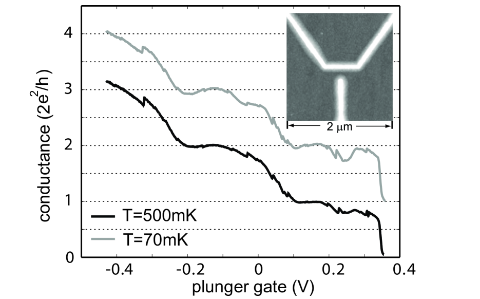
We fabricated a quantum point contact (QPC) with a lithographic width of 165 nm and tested its electronical functionality by measuring its conductance at low temperatures (Fig. 1). At the temperature of 500 mK quantized conductance plateaus are observed corresponding to transmission of one and two modes through the QPC. In addition, a plateau-like structure is observed at . As the temperature is reduced to mK, this plateau-like feature evolves into a dip-like structure below the first plateau (Fig. 1). In differential conductance vs. bias measurements we observe a pronounced zero-bias peak for a QPC conductance , which weakens as the conductance increases to , and completely disappears above the first plateau. This behavior might indicate that the structure below the first plateau is related to Kondo-like effect Cronenwett02 . Besides, at T mK another plateau-like structure at appears. All features observed in this sample were stable and reproducible in several different cool-downs.
Hole transport in p-type GaAs quantum dots is also explored. Two quantum dots were fabricated with AFM lithography - one rectangular (Fig. 2(b)) with lithographic dimensions nm2, and the other circular (Fig. 2(d)) with lithographic radius nm. The transport measurements in both dots have been performed in a dilution refrigerator at a base temperature of 70 mK. We have measured the two-terminal conductance of the dots by applying either a small dc or ac bias voltage Vbias between source and drain, and measuring the current through the dot with a resolution better than 50 fA.
The QPC gates are tuned to configurations where the dots are symmetrically coupled to the leads. Pronounced Coulomb resonances are observed in both dots (Fig. 2(a) shows Coulomb peaks from the rectangular dot). It is important to note that the dots close when the value of the plunger-gate voltage increases this is a clear indication that we measure hole transport. Coulomb resonances are fitted both with an expression for a thermally broadened Coulomb blockade peak in the multi-level transport regime and a coupling broadened Lorentzian peak. In all cases the thermally broadened resonance fits better to the data than a coupling broadened resonance, indicating that the dots are in the weak coupling regime. The electronic temperature extracted from the fitting is 130 mK.
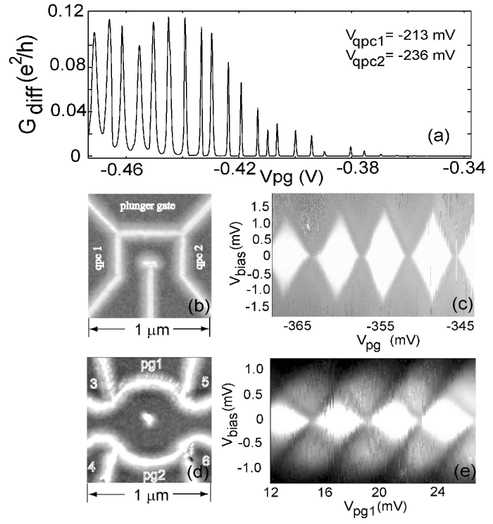
Coulomb diamond measurements are performed in the weak coupling regime for both dots, and the results are shown in Fig. 2. The uniform size of the diamonds indicates that all confined holes reside in one single potential minimum rather than occupying several disconnected or tunnel-coupled potential minima. From the extent of the diamonds in bias direction we estimate a charging energy of the rectangular dot to be meV, while the lever-arm of the plunger gate is . In case of the circular dot we obtain meV and . Assuming a disk-like shape of the dots allows us to estimate electronic radius of the dots from the values of their charging energies. The obtained value for the rectangular dot is nm, and for the circular nm, which is consistent with the lithographic dimensions of the dots and indicates that the dots are really formed in the regions encircled by the oxide lines.
Due to the large effective mass of holes, the single-particle level spacing in case of hole quantum dots is significantly smaller compared to electron quantum dots with similar size. The estimated mean single-particle level spacing in the rectangular dot is eV, and in the circular dot is eV. Therefore we were not able to resolve excited states in Coulomb diamond measurements in neither of the two dots. This fact, together with the observed temperature dependence of Coulomb peak heights Grbic05 indicates that both dots are in the multi-level transport regime. In order to be able to investigate the single-particle level spectrum in hole quantum dots, one has to significantly reduce the lateral dimensions of the dot as well as the hole temperature.
In conclusion, we fabricated tunable nanodevices on p-type GaAs heterostructures by AFM oxidation lithography. By using this fabrication technique we were able to overcome the problems with large hysteresis effects present in gate sweeps in conventional split-gate defined nanostructures on p-type GaAs, and the stability of the structures improved as well. Electronic functionality of these structures was demonstrated by observing conductance quantization in a QPC, and Coulomb blockade in two quantum dots with different geometries. Further reduction in size of the p-type quantum dots is necessary in order to explore the influence of spin-orbit and carrier-carrier interactions on single-particle level spectra.
Financial support from the Swiss National Science Foundation is gratefully acknowledged.
References
- (1) R. Winkler, Springer Tracts in Modern Physics, Volume 191, Springer-Verlag (2003)
- (2) B. Grbić et al., Appl. Phys. Lett. 85, 2277 (2004)
- (3) R. Held et al., Appl. Phys. Lett. 73, 262 (1998).
- (4) L. P. Rokhinson et al., Superl. and Microstr. 32, 99 (2002).
- (5) B. Grbić et al., Appl. Phys. Lett. 87, 232108 (2005)
- (6) S. Cronenwett et al., Phys. Rev. Lett. 88, 226805 (2002)