Electric-field controlled spin reversal in a quantum dot with ferromagnetic contacts
Manipulation of the spin-states of a quantum dot by purely electrical means is a highly desirable property of fundamental importance for the development of spintronic devices such as spin-filters, spin-transistors and single-spin memory as well as for solid-state qubits ref:Wolf01 ; ref:Awschalom07 ; ref:Ohno00 ; ref:Recher00 ; ref:Folk03 ; ref:Elzerman04 . An electrically gated quantum dot in the Coulomb blockade regime can be tuned to hold a single unpaired spin-, which is routinely spin-polarized by an applied magnetic fieldref:Lindelof02 . Using ferromagnetic electrodes, however, the properties of the quantum dot become directly spin-dependent and it has been demonstrated that the ferromagnetic electrodes induce a local exchange-field which polarizes the localized spin in the absence of any external fields ref:Ralph04 ; ref:Martinek03a . Here we report on the experimental realization of this tunneling-induced spin-splitting in a carbon nanotube quantum dot coupled to ferromagnetic nickel-electrodes. We study the intermediate coupling regime in which single-electron states remain well defined, but with sufficiently good tunnel-contacts to give rise to a sizable exchange-field. Since charge transport in this regime is dominated by the Kondo-effect, we can utilize this sharp many-body resonance to read off the local spin-polarization from the measured bias-spectroscopy. We show that the exchange-field can be compensated by an external magnetic field, thus restoring a zero-bias Kondo-resonance ref:Martinek03a , and we demonstrate that the exchange-field itself, and hence the local spin-polarization, can be tuned and reversed merely by tuning the gate-voltage ref:Martinek05 ; ref:Sindel07 . This demonstrates a very direct electrical control over the spin-state of a quantum dot which, in contrast to an applied magnetic field, allows for rapid spin-reversal with a very localized addressing.
Since the discovery of carbon nanotubes they have been intensively studied for their unique electrical properties. Their high Fermi-velocity and small spin-orbit coupling make them particularly well-suited for spintronics applications utilizing the transformation of spin-information into electrical signals. Spin-valve effects in nano-junctions with a carbon nanotube (CNT) spanning two ferromagnetic electrodes have already been observed ref:Sahoo05 ; ref:Jensen05 ; ref:Hueso07 , and a strong gate-dependence of the tunnel magneto-resistance has been demonstrated for carbon nanotube quantum dots in both the Coulomb blockade, and the Fabry-Perot regime ref:Sahoo05 .
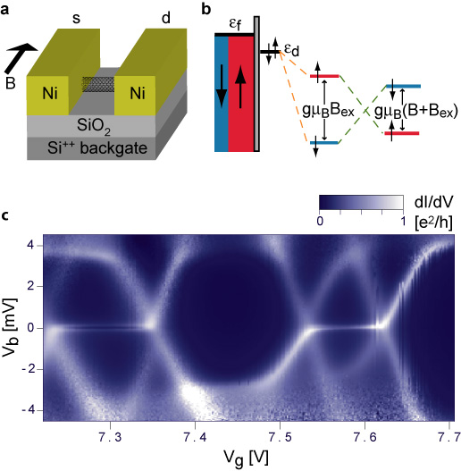
In the intermediate coupling regime, odd numbered quantum dots exhibit the Kondo effect seen as a pronounced zero-bias conductance peak at temperatures below a characteristic Kondo temperature, ref:Glazman88 ; ref:Goldhaber98 ; ref:Lindelof00 . This effect relies on the conduction electrons being able to flip the spin of the dot during successive cotunneling-events and is therefore expected to be sensitive to spin-polarization of the electrodes. As pointed out by Martinek et al. ref:Martinek03a , quantum charge-fluctuations of the dot will renormalize the single-particle energy-levels in a spin-dependent manner and thereby break the spin-degeneracy on the dot, causing the zero-bias Kondo peak to split in two. This tunneling-induced exchange-field splitting has since been seen by Pasupathy et al. ref:Ralph04 in an electromigrated Ni-gap holding a -molecule.
A singly occupied level residing just below the Fermi-energy of the leads is strongly shifted by virtual tunneling out of the dot, whereas a level deep below the Fermi-energy (by almost the charging-energy) is shifted by tunneling of electrons into the dot. For spin-polarized electrodes having a difference in the density of spin-up, and spin-down states, this implies a spin-splitting of the dot level where sign and size depends on the applied gate-voltage, i.e. the position of the level below the Fermi-energy. At the particle-hole symmetric point right between the empty and doubly occupied states the spin-degeneracy is expected to be intact ref:Choi04 . In a material like Ni, however, one expects the band structure to be energy dependent and to have a Stoner splitting, this will break the particle-hole symmetry and therefore shift the spin-degeneracy point away from the middle of the diamond ref:Martinek05 ; ref:Sindel07 . Basically all the theoretical predictions for this pronounced gate-dependence of the local spin-states are experimentally verified by the transport-measurements presented below.
The CNTs were grown by chemical vapor deposition on a SiO2 wafer with a highly doped Si back-gate. The ferromagnetic leads were made of pure Ni in strips of thickness 60 nm, widths 300-1000 nm and separated by 200-400 nm. All measurements were made in a 3He/4He dilution refrigerator, with a base-temperature of 30 mK, corresponding to a minimum electron temperature of 80 mK, and using a standard AC-setup with asymmetric bias. A magnetic field was applied in the direction of the Ni-leads in the plane of the electrodes as shown in figure 1a. We observe a clear even-odd effect with a zero-bias anomaly in every second Coulomb diamond indicating a spin-1/2 Kondo effect with a typical Kondo temperature, K. Many of the observed Kondo anomalies showed a gate-dependent splitting and here we discuss two different devices for which this dependence is particularly clear, in the supplement two other examples are shown.
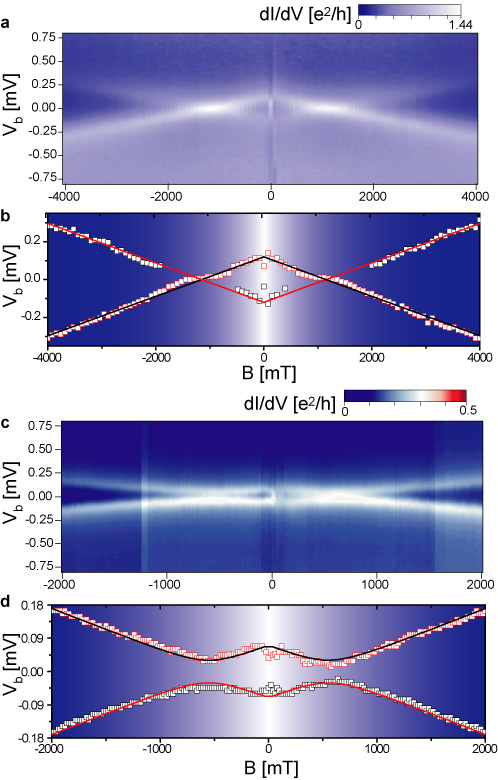
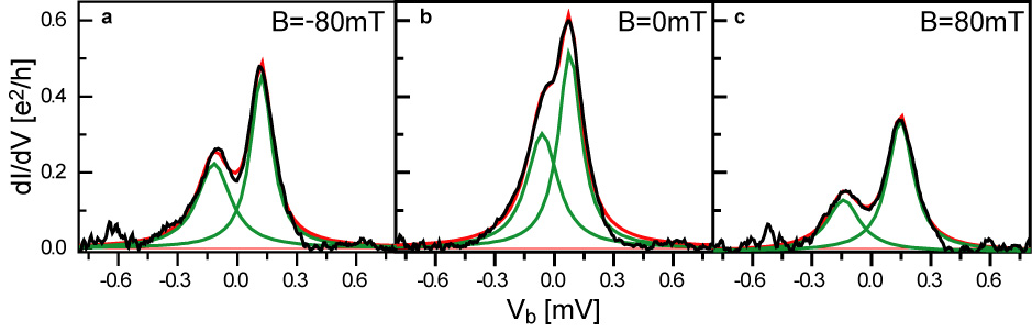
Magnetic force microscopy images of devices similar to the ones measured indicate that the CNT quantum dot is most likely coupled to one single domain in both source, and drain electrode. Applying a strong magnetic field serves partly to align the two contact-domains and partly to provide a Zeeman-splitting of the local spin. Figure 2 shows the conductance vs. bias-voltage and external field, measured for a gate-voltage tuned to the middle of an odd occupied Coulomb blockade valley in the Kondo regime. Device 1 (figure 2a,b) shows a simple linear behavior in which the single-domain magnetization and hence the exchange field, , is aligned with the external field, . The exchange field can therefore be completely compensated and the zero-bias Kondo peak is seen to be restored at T, giving an indirect measure of the exchange-field at this gate-voltage. In device 2 (figure 2c,d), on the other hand, the Kondo peak is never fully restored and the splitting merely reaches a minimum at T. This indicates that the exchange-field lies at an angle to the external field, and fitting the B-dependence of the peak-splitting by , we find this angle to be (cf. supplementary material).
Figure 2 was recorded by sweeping the field from large negative to large positive values, a sudden decrease(increase) of the splitting is clearly visible at small negative(positive) fields. A similar switching was observed in Ref. ref:Ralph04, and can be ascribed to a sudden switching from parallel (P) to anti-parallel (AP) configuration of the contact-domains driven by domain interactions (cf. supplementary material). In the AP-configuration the tunnel-induced exchange-field is nearly canceled, unless the couplings to source, and drain-electrodes are very different. In terms of the conduction-electron spin-polarization, , and the tunnel-broadening, , where denotes the density of states (DOS) in the leads and is the tunneling amplitude to source(drain), one expects ref:Ralph04 ; ref:Utsumi05 that . Comparing now the exchange-fields in P, and AP-configuration we deduce that , this corresponds to a zero-bias Kondo peak height of roughly consistent to the value of , measured on device 1 in the middle of the Coulomb blockade diamond for a fully compensating magnetic field near 1.12 T.
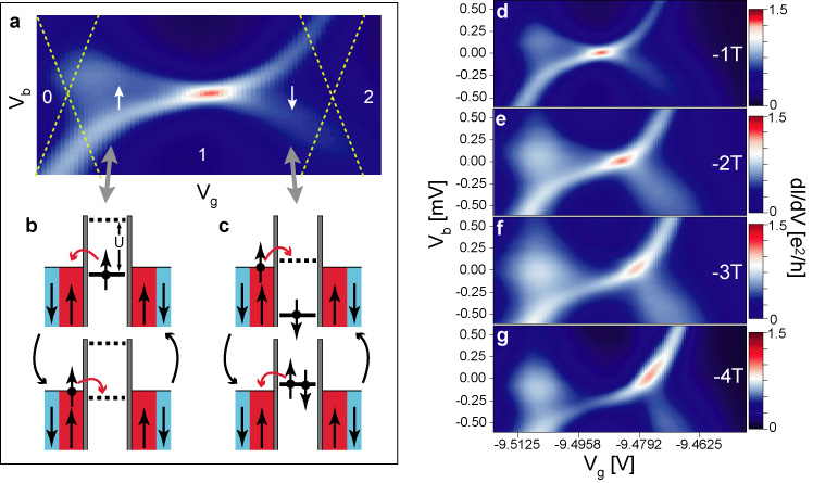
In a Coulomb blockade diamond with an odd number of electrons, the left, and right charge-degeneracy points correspond to respectively emptying the dot or filling it by one extra electron. With a finite spin-polarization in the leads, tunneling of majority-spins, spin-up say, will be favored by the higher-density of states and a dot-state of spin-up will therefore be shifted further down in energy than a spin-down state, as long as one is closer to the left hand side (l.h.s.) of the diamond. Due to the Pauli-principle, the majority-spins can only tunnel into the dot if the residing electron is in a spin-down state. It is therefore the spin down state which is lowered the most near the right hand side (r.h.s.) of the diamond. This simple mechanism of level-renormalization, illustrated in figure 3a-c, is encoded in the exchange-field, given to good accuracy by
| (1) |
to leading order in the tunneling-amplitude ref:Sindel07 and assuming a constant density of states. is the charging-energy and is the dot-level-position which is proportional to the gate-voltage. Notice the strong negative and positive logarithmic corrections for close to or , respectively (corresponding to left, and right borders of the diamond). In the middle of the diamond, , the exchange-field is zero except for a constant term, , which reflects a Stoner-splitting between the spin-up and spin-down bands ref:Martinek05 ; ref:Sindel07 . Notice that possible stray-fields from the magnetic contacts would also contribute with a gate-independent spin-splitting (cf. supplementary material).
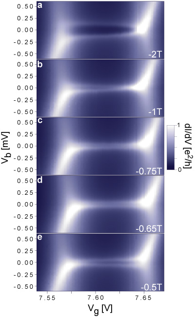
Depending on the magnitude of , Equation (1) predicts a change of the ground state spin direction as the localized level is moved from to . Such a spin reversal can be observed in figure 3d-g and occurs where the Kondo ridges cross and the spin states are degenerateref:footnote . The movement of the conductance peak (red dot) as function of magnetic field, seen in figure 3d-g, confirms that the ground-state spin can indeed be reversed by changing the gate-voltage. Furthermore, the direction of the motion shows that it is predominantly spin-up (i.e. the spin along the external magnetic field) electrons which tunnel on and off the dot, giving a ground-state with spin-up at the l.h.s of the diamond and spin-down at the r.h.s. This confirms earlier observations in conventional superconducting tunnel-junctions ref:Tedrow71 ; ref:Kim04 indicating that the tunneling electrons in Ni have majority-spin, i.e. positive polarization. Most likely, the more mobile -electrons taking part in the tunneling are spin-polarized by their hybridization with the localized -electrons ref:Tsymbal97 ; ref:Mazin99 .
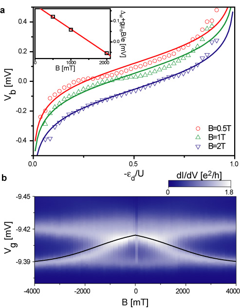
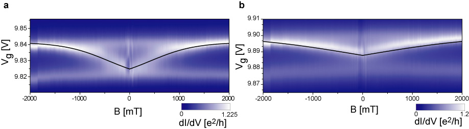
In order to substantiate the detailed gate-voltage dependence of the exchange-field, we have extracted the peak-positions from plots like those in figures 3d-g and fitted them by with given by equation (1). The result is shown in figure 4a where the inset shows as a function of . The slope of the line corresponds to as expected for a carbon nanotube. The white ridge in Figure 4b traces the magnetic field dependence of the gate-voltage at which the spin states are degenerate, showing a gratifying resemblance to the theory-plots presented in Refs. ref:Martinek05, ; ref:Sindel07, . Inverting equation (1) and using the fitting-parameters deduced from figure 4a, we arrive at the parameter free fit seen as the black line in figure 4b.
References
- (1) Wolf, S. A. et al. Spintronics: a spin-based electronics vision for the future. Science 294, 1488-1495 (2001).
- (2) Awschalom, D. D. & Flatté, M. E. Challenges for semiconductor spintronics. Nature 3, 153 (2007).
- (3) Ohno, H., et al. Electric-field control of ferromagnetism. Nature 408, 944 (2000).
- (4) Recher, P., Sukhorukov, E. V. & Loss, D. Quantum Dot as Spin Filter and Spin Memory. Phys. Rev. Lett. 85, 1962 (2000).
- (5) Folk, J. A., Potok, R. M., Marcus, C. M. & Umansky, V. A Gate-Controlled Bidirectional Spin Filter Using Quantum Coherence. Science 299, 679 (2003).
- (6) Elzerman, J. M., Hanson, R., Willems van Beveren, L. H., Witkamp, B., Vandersypen, L. M. K. & Kouwenhoven, L. P. Single-shot read-out of an individual electron spin in a quantum dot. Nature 430, 431 (2004).
- (7) Lindelof, P. E., Borggreen, J., Jensen, A., Nygård, J. & Poulsen, P. R. Electron Spin in Single Wall Carbon Nanotubes. Physica Scripta T102, 22 (2002).
- (8) Patsupathy, A. N. et al. The Kondo effect in the presence of ferromagnetism. Science 306, 86 (2004).
- (9) Martinek, J. et al. Kondo effect in Quantum Dots coupled to Ferromagnetic Leads. Phys. Rev. Lett. 91, 127203 (2003).
- (10) Martinek, J. et al. Gate controlled splitting in quantum dots with ferromagnetic leads in the Kondo regime. Phys. Rev. B 72, 121302 (2005).
- (11) Sindel, M. et al. Kondo quantum dot coupled to ferromagnetic leads: a study by numerical renormalization group technique. Phys. Rev. B 76, 45321 (2007).
- (12) Sahoo, S. et al. Electric field control of spin transport. Nature Physics 1, 99 (2005).
- (13) Jensen, A., Hauptmann, J. R., Nygård, J. & Lindelof, P. E. Magnetoresistance in ferromagnetically contacted single-wall carbon nanotubes. Phys. Rev. B 72, 35419 (2005).
- (14) Hueso, L. E. et al. Transformation of spin information into large electrical signals using carbon nanotubes. Nature 445, 410 (2007).
- (15) Glazman, L. & Raikh, M. Resonant Kondo transparency of a barrier with quasilocal impurity states. JETP Letters 47, 452-455 (1988).
- (16) Goldhaber-Gordon, D. et al. Kondo effect in a single-electron transistor. Nature 391, 156 (1998).
- (17) Nygård, J., Cobden, D. H. & Lindelof, P. E. Kondo physics in carbon nanotubes. Nature 408, 342 (2000).
- (18) Choi, M. S., Sanchez, D. & Lopez, R. Kondo effect in quantum dot coupled to ferromagnetic leads: a numerical renormalization group analysis. Phys. Rev. Lett. 92, 56601 (2004).
- (19) Utsumi, Y., Martinek, J., Schön, G., Imamura, H. & Maekawa, S. Nonequilibrium Kondo effect in a quantum dot coupled to ferromagnetic leads. Phys. Rev. B 71, 245116 (2005).
- (20) Note that these plots have been recorded prior to a switch in device 1, whereas all other measurements taken on device 1 were recorded after. We present these plots since they bring out most clearly the movement of the degeneracy point. The corresponding plots recorded after the gate-switch are shown in the supplementary material and are qualitatively similar
- (21) Tedrow, P. M. & Meservey, R. Spin-Dependent Tunneling into Ferromagnetic Nickel. Phys. Rev. Lett. 26, 192 (1971).
- (22) Kim, T. H. & Moodera, J. S. Large spin polarization in epitaxial and polycrystalline Ni films. Phys. Rev. B 69, 20403(R) (2004).
- (23) Mazin, I. I. How to Define and Calculate the Degree of Spin Polarization in Ferromagnets. Phys. Rev. Lett. 83, 1427 (1999).
- (24) Tsymbal, E. Y. & Pettifor, D. G. Modelling of spin-polarized electron tunnelling from 3d ferromagnets. J. Phys.: Condens. Matter 9, L411 (1997).
Acknowledgements
We thank R. Gunnarsson, L. Borda, K. Flensberg, P. Hedegård, and C. M. Marcus for discussions. For financial support we thank Danish Agency for Science Technology and Innovation (FTP 274-05-0178) and EU projects SECOQC and CARDEQ.
Competing financial interests
The authors declare that they have no competing financial interests.
Supplementary material for ”Electric-field controlled spin reversal in a quantum dot with ferromagnetic contacts”
I Domain switching and stray-fields
Magnetic force microscopy images of devices similar to the ones measured, reveal a typical domain-size of , which suggests that the carbon nanotube quantum dot is most likely coupled to one single domain in both source, and drain electrodes. Using the saturation magnetization for Ni, , the magnetic moment of a single contact-domain can be estimated by . With 200 nm between the electrodes, this gives a crude estimate of the dipole-dipole interaction energy of the two contact-domains with an energy-gain of roughly 200 eV between the parallel (P) and anti-parallel (AP) configurations. Starting in the P-configuration for a large applied magnetic field, this in turn implies a transition to AP-configuration once the external field becomes smaller than some 30 mT. The switching from P to AP observed in article-figures 2a,c occurs at fields smaller than 80 mT for device 1 and close to 40 mT for device 2. Article-figures 2a,c were recorded with a resolution in of 80 mT and 10 mT, respectively. This simple estimate of course neglects all intra-lead domain-interactions, which cannot a priori be assumed to be less important.
From this we can also estimate the stray-field at the middle between the two electrodes. In the AP-configuration it is close to zero and in the P-configuration it must be roughly mT, i.e. a factor of 10 and 5, respectively, smaller than the tunneling-induced exchange-fields which we read off from article-figures 2a,c. We note that this rather crude estimate is comparable in magnitude to the estimates made in Refs. ref:sRalph04, ; ref:sSahoo05, ; ref:sMeier06, . Notice also that stray-fields cannot account for the gate dependence observed in article-figures 3d-g.
The fact that the exchange-field cannot be completely compensated by the external field in device 2 is interpreted as a misalignment of and . Since bulk Ni has only weak magnetic anisotropy, this is most likely due to the reduced geometry and surface roughness of the leads. The fit shown in article-figure 2d takes a fixed direction of the magnetization which is found to be . We have also tried to make another fit with a finite anisotropy barrier, using a simple Stoner-Wohlfarth model where the magnetic energy of the system is given by
| (2) |
in terms of applied field and magnetization at a relative angle , together with an angle between an easy-axis and the applied field. parameterizes the anisotropy barrier, thus allowing the magnetization to align with for large enough values of . Minimizing this energy as a function of angle for a given applied field gives a hysteretic magnetization curve from which we can then infer the sum of applied, and exchange-field to determine the spin-splitting as a function of . Nevertheless, this fit performed no better than the far simpler fit to a fixed angle.
II Additional plots for devices 1 and 2
II.1 Device 1
The ratio of the couplings to respectively source and drain electrodes can be estimated from the formula
| (3) |
where () denotes the splittings in the parallel (antiparallel) configuration which are read off from figure 5. This gives the estimate , cited in the main paper.
The plots in figure 6 shows the differential conduction as a function of gate and bias voltage measured at different magnetic fields. The measurements are made on device 1 after a switch, i.e. a sudden, permanent change in the device behavior. Notice that the crossing of the Kondo ridges moves from left to right as the magnetic field is increased. It is these measurements that the scatter and fits in article-figure 4a are made from. Note that the plot measured at T has also been fitted but is not shown in article-figure 4a since it is placed right on top of T. The plot made at T is not included in the fitting since the domain configuration is expected to be different. The point corresponding to T in the inset of article-figure 4a is really the average of the fitted constants, 0.065 mV and 0.053 mV, obtained at T and T, respectively.

II.2 Device 2
The plot shown in figure 7 shows the differential conductance as a function of gate, and bias voltage measured at different magnetic fields. The slopes of the Kondo ridges in a, b and in e are clearly opposite, although the measurements at intermediate magnetic fields (c, d) show no crossing of the Kondo ridges. We ascribe this to a misalignment of the domain magnetization direction (and therefore the exchange field) and the external magnetic field.
III Plots for devices 3 and 4
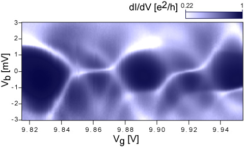
Figure 8 shows the differential conduction as a function of gate, and bias voltage. Two Kondo ridges near zero bias can be observed and henceforth we shall refer to the corresponding odd-numbered Coulomb-blockade diamonds as devices 3 and 4, respectively. These measurements are made on the same sample as device 1 but off-set in gate voltage by roughly 20 V.
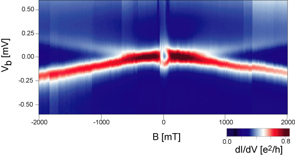
Figure 9 shows as a function of bias voltage and magnetic field. The measurements are made close to the middle of the Coulomb-blockade diamond in device 3. A linear splitting of the Kondo peak with magnetic field can be observed, as would be expected since this device should be contacted by the same domains as device 1 and the domain configuration and magnetization direction in the leads should be independent of the gate voltage.
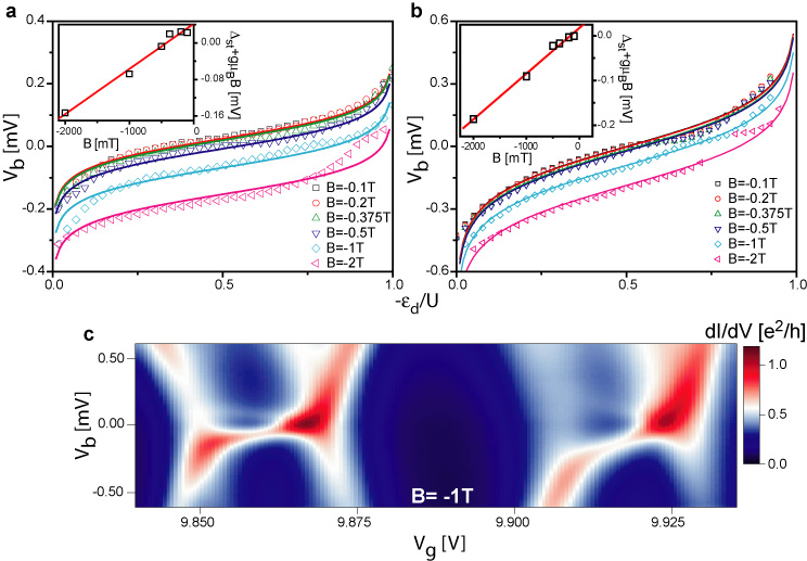
Figure 10c shows a zoom-in on the Kondo ridges, measured at T. A gate dependent splitting of the Kondo resonance is clearly observed in both device. The different slopes indicate a change in from one Kondo resonance too the next, most likely due to a difference in couplings to the two orbitals in the CNT.
The splittings of the Kondo peaks have been read off and plotted in figure 10a,b. The lines are fits to the scatter-plots and the different colors correspond to different external magnetic fields. The fitted values used for are 0.045 and 0.117 meV for the groups of fits in a and b, respectively. The insets in both figures show as function of . The two linear fits yield a slope of 9.9 (a) and (b ), corresponding to a -factor of 1.7 and 1.8, respectively.
References
- (1)
- (2) Patsupathy, A. N. et al. The Kondo effect in the presence of ferromagnetism. Science 306, 86 (2004).
- (3) Sahoo, S. et al. Electric field control of spin transport. Nature Physics 1, 99 (2005).
- (4) Meier, L., Salis, G., Ellenberger, C., Ensslin, K., Gini, E. Stray-field-induced modification of coherent spin dynamics. Appl. Phys. Lett. 88, 172501 (2006).
- (5)