Negative Differential Spin Conductance by Population Switching
Abstract
An examination of the properties of many-electron conduction through spin-degenerate systems can lead to situations where increasing the bias voltage applied to the system is predicted to decrease the current flowing through it, for the electrons of a particular spin. While this does not necessarily constitute negative differential conductance (NDC) per se, it is an example of negative differential conductance per spin (NDSC) which to our knowledge is discussed here for the first time. Within a many-body master equation approach which accounts for charging effects in the Coulomb Blockade regime, we show how this might occur.
I introduction
Nonequilibrium properties like electronic conduction in molecular systems must be treated within a many-body nonequilibrium theory, and the extensive body of effects such treatments produce has attracted many research efforts on both the theoretical and experimental sides.Dekker1999 ; Tour2000 ; Ratner2000 ; Joachim2000 ; Avouris2002 ; Nitzan2003_1 ; Heath2003 ; Datta2004 ; Hod2006a In particular, models of transport through molecules and quantum dots have been shown to describe many nontrivial phenomena, of which the Coulomb Blockade effect is a well known example.Elhassid00 Such models have been shown to describe cases where an increase in the source-drain bias on a small device coupled to macroscopic leads actually results in a decrease of the current through it.Ratner96 ; Lang97 ; Xue99 ; Heij99 ; Larade01 ; Rogge06 This nonlinear behavior is known as negative differential resistance or conductance (NDR or NDC), and its explanation must lie in the shifted states of the system and the switching of electron populations between them, but the exact mechanism may differ between the various cases.
Several such mechanisms, many of which are actually single-electron effects, are worth noting: the resonant double-barrier tunneling junction familiar in doped semiconductor work,Carroll63 where an increasing bias pushes a resonant conduction state into the conduction window and then out of the conduction band of one of the electrodes, resulting in NDR;Larade01 the case in which the electrodes themselves have narrow resonant features in their density of states, like an atomic-scale STM tip or an atom weakly coupled to a larger electrode, where the bias shifts the conducting levels of the electrodes into and out of alignment with each other;Avouris89 ; Lang97 ; Xue99 the Coulomb-Blockade case where the bias charges the system in a way that kicks a level out of the conduction window;Uozumi95 ; Shin98 ; Heij99 the more general case where the biasing actually conforms the molecule or causes a change in the interaction with phonons,Reed99 ; Nitzan04 ; Ratner04 ; Nitzan07 resulting once again in fewer available conduction levels.
When the situation is complicated by the lifting of spin degeneracy, the interplay between the occupation of spin levels and their coupling to the leads can result in spin-dependent effects as well. This has often been explored in cases where the leads are ferromagnetic,Awschalom01 ; Zutic04 for example in the spin-blockade or spin field effect transistor.Datta90 More recently, spintronics without polarized leads have been suggested,Takayanagi99 ; Richter01 ; D'Amico03 ; Richter03 ; Vasilopoulos04 ; Richter04a ; Richter04b ; Richter04c ; Sigrist05 ; Vasilopoulos05 ; Peeters06 ; Perroni06 ; Cohen07 where the leads would generally contain electrons of both spins, which would scatter through the system with different transmission properties. In a practical application the device might perform various transformations on spins rather then just act as a current switch. Thus it makes sense to develop the concept of conduction or resistance per spin, with the understanding that the same range of nonlinear phenomenon that is of interest for the total current can occur here for spin-dependent current. Specifically, the study of NDC is naturally complemented by NDC per spin, which is exhibited whenever increasing the bias voltage on a conducting device causes the current through it for one spin to decrease, while the total current does not necessarily decrease.
In this paper we take an illustrative look at a novel mechanism for the phenomenon of negative differential spin conduction (NDSC). We show that in cases where the charging of a quantum dot is a dominant energy scale of the problem and the spin degeneracy is lifted, NDSC can occur. The basic mechanism involves population switching between the two spin levels. In Section II we describe a simple device in which NDSC may appear and be of interest, and explain the multi-electron master equation approach we employ for calculating the spin-polarized current. In Section III we display and analyze the results. Finally, we discuss our conclusions in Section IV.
II Model
Perhaps the simplest and most abstract spintronic device one might imagine consists of a system with a single (energetically relevant) electron level coupled to two metallic leads. By making this level non-degenerate in the spin degree of freedom in any desired way, one can achieve filtering behavior by tuning the conduction window so as to contain only one of the spin levels.Takayanagi99 ; Richter03 ; Vasilopoulos04 ; Peeters06 ; Cohen07 If the system is small, one expects that the charging should become an important energy scale in the problem, and the population of electrons the device contains at any given time should not vary greatly from the neutral number of electrons. At this regime a many-electron master equation treatment Beenakker91 ; Kinaret92 ; Bonet02 ; Hettler03 ; Datta2004 ; Elste05 ; Braig05 ; Mukamel06 ; Hanggi2006 ; Nitzan07 can be expected to provide a good approximation of the dynamics, particularly for larger voltages.
We consider a model for a spin-filter device which is described by a two single spin levels. Such a device can be an atom, a molecule, a quantum dot, or any system with discrete levels that are well separated. The single electron levels on the device are coupled to two leads with chemical potentials and and coupling constants , which we will assume to be equal to . The model Hamiltonian of such a device (not including the leads, since the current and level populations will be calculated within a standard multi-electron master equation approach)Datta2004 is given by:
| (1) |
where and are single particle annihilation operators corresponding to the two spin levels ( and , respectively) and is the neutral number of electrons. We also introduce the spinless level energy , the spin energy shift and the charging energy . We note in passing that the notation is only for convenience and no real assumptions are made as to the symmetry of the shift. In fact, the results are relevant to any two separate channels with different energies, for instance two quantum dots of slightly different energies each of which is coupled to different leads with a charging interaction between them.
We now describe the approach taken to construct the multi-electron master equation, suitable for the above model, from single electron data. If one neglects spin-dependent multi-electron effects, then it is formally straightforward to build from a set of one-electron Hamiltonian and spin eigenfunctions an anti-symmetric basis of multi-electron wavefunctions. Limiting the discussion to only two levels, one can define:
| (2) |
Here is the two particle anti-symmetrization operator and the states are identified by their (spin-dependent) level occupations ( or for fermions). Using this anti-symmetric multi-electron wavefunction we can uniquely and conveniently determine the nonzero matrix elements of a general many-body operator required to construct the master equation. According to the Slater-Condon rules where only single electron integrals are taken into account:
| (3a) | |||
| (3b) | |||
| (3c) | |||
| (3d) | |||
Multi-electron effects will be considered only in the form of charging energy. Since these values will be used in a rate-process calculation rather than a full quantum formulation, constructing the multi-electron states themselves is actually redundant, and Eqs. (3b)-(3d) along with the single particle data will provide all the necessary information.
The transfer rates between the multi-electron states are given by:Datta2004
| (4) |
where the four multi-electronic states are labeled by the Greek indices and , such that (for instance) is the empty state, is the state where only level is occupied, and is the state where only level is occupied. The lead index in the above is . For reasons that will become clear below, we also define the total transfer rate summed over both leads:
| (5) |
Following the Slater-Condon rules (cf., Eqs. (3c) and (3d)), the coupling between the multi-electron states, , is related to the single electron level coupling (or the imaginary part of the self-energy)Datta_book and is given by if the two multi-electronic states differ only by the occupation of level , if they differ only by and and , and otherwise. As noted above, is the matrix element of the single electron level coupling. in Eq. (4) is related to the Fermi-Dirac function, :
| (6) |
where is the number of electrons in state . The state energies are calculated from the Hamiltonian (1) and amount to , , and respectively for the states , , and .
Once the rates are known, the linear master equation system can be read from the detailed-balance condition for steady-state:
| (7) |
where is the probability that the system is in a multi-electron state . The current at steady state is given in terms of the steady state occupation probabilities and can be expressed as Datta2004 :
| (8) |
where
| (9) |
Intuitively, this expression states that current flows out of lead whenever an electron flows from it into the device, with the inverse also true. Following a similar line of physical reasoning leads to an expression for spin-polarized current: up or down current flows out of lead whenever an up or down electron flows from it into the device. Assuming no coupling between levels with different spin, the spin-dependent current is given by:
| (10) |
and
| (11) |
Here, where for spin up () or down (), respectively.
The linear master equations can be solved analytically, but the form of the solution is rather cumbersome and has no real benefit. They can also, of course, be solved numerically, which is the method chosen for this work.
III Results and Analysis
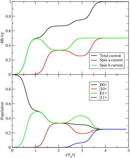
As the above model is more or less identical to the one commonly used to explain the Coulomb blockade, it is no surprise that plotting the characteristics of the system shown in the upper panel of Fig. 1 immediately displays the well-known nonlinear current steps typical of Coulomb blockade effect.Elhassid00 The model parameters used here are , , , and . The neutral number of conduction electrons has been taken to be . Conduction peaks or rises in the total current are expected in this formalism when there exists an energy difference between two states with electronic occupations that differ by one (), which is also the energy of an electron occupied in one lead but not the other (when ). In other words, the total current can rise at any bias voltage where the conduction window is expanding so as to contain some spectral line of the system. For the present model, this occurs when
| (12) |
This is clearly the case for the current shown in the upper panel of Fig. 1, where the four steps observed in the total current appear at , , , and corresponding to transitions between states , , , and , respectively and according to Eq. (12).
Turning now to discuss the current per spin also shown in the upper panel of Fig. 1, we still observe the Coulomb blockade steps, however, the direction of the step can be either positive or negative. This is an example of a negative differential spin conduction where an increase of the bias voltage is followed by a decrease in the current per spin. The NDSC occurs for both spins in this case, and at a different bias voltage for each spin-current. The first drop in current occurring for spin type is also accompanied by a sudden drop in the population of the state (shown in the lower panel of Fig. 1), as the change in chemical potentials begins to allow the population of the state. This switching of populations between the states is reminiscent of another example of nonmonotonic changes in occupation predicted to occur in a system of two electrostatically coupled single-level quantum dots.Gefen05 ; Oreg05 .
There is a simple “hand waving” explanation for such behavior: the current for each spin consists at low bias of contributions proportional to the probability that the system is in some state and to the rate of transitions between state and state (in which none of the states are occupied), where can be either for spin up current or for spin down current. We therefore expect that at any chemical potentials where the relevant Fermi functions and hence the rates are nearly constant at the relevant energy, the current will, to a good approximation, be linearly proportional to the population. The population, in turn, decreases whenever the shifted energetics allow the occupation of a new state. For this to be possible, the bias must be applied in such a way that not all states become occupied simultaneously. This is the reason the central chemical potential has been placed below the levels.The second current drop in the figure, which occurs at higher voltage and for the spin current, can be explained by a similar argument - this time, however, the depopulation of the state is the one involved.
It is worth pointing out that the population shifts are such that in regions where the chemical potentials are far from any levels, any states that energetically can be populated become so with equal probability. At low bias only one state has the entire population, then as the bias is increased the population is shared equally between two states, then between three, and finally between all four states. This is the cause of the downward shifts in the population which result in the NDSC. For the example shown in Fig. 1 conduction sets in when the population of state decreases from its maximal value of until both states and are equally populated. Then NDSC occurs when both states and lose population to state until all three state become equally populated. It is also evident that in systems with more electronic levels, NDSC due to population switching will become weaker if the separation between the states is small. Noticing this fact also clarifies the role of charging in NDSC, as without charging all the states which include the same energetically occupiable levels would become populated at the same bias voltage.
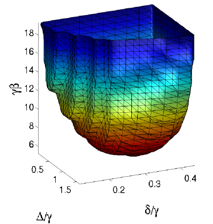
The theoretical phenomenon of NDSC and its physics are easy to understand, and the mechanism we suggest for it here simple, but two important questions remain: when will it occur, and how can it be observed experimentally? Answering the first question formally is a matter for the analysis of the expressions for the spin currents: by taking their derivatives and looking for a local maximum in the voltage, an exact condition could be worked out in principle. In practice, the analytical development involves the solution of nonlinear equations, may or may not be possible and of interest, and is beyond the scope of the present work. Instead, a look at a part of the surface of transition in parameter space between regions where NDSC does and does not appear (see Fig. 2) is enough to convince oneself that the exact conditions for NDSC are nontrivial. If one is more interested in the approximate limits where the drop in the current constitutes a sizable fraction of its maximum value and where the master equation is valid, these can be expected when the temperature is smaller than the splitting between the spin states, ; when the conduction resonances are narrow enough such that ; and when the charging energy is of the order of the level spacing, . All criteria can be met, for example, for systems of nanometer dimensions where the charging energy and the level spacing can be tuned by simple changing the size. Also, as mentioned above, some asymmetry in the application of the chemical potential and/or bias voltage is required, as the spin dependent effects happen to cancel out completely when the chemical potential is exactly between the energies of the two levels and the bias is applied symmetrically. In addition, NDSC requires some state to become energetically occupiable at a bias voltage higher than one at which a spin current exists. More precise conclusions require a calculation similar to the one done to produce Fig. 2, which takes negligible computational effort and can be easily extended to more detailed scenarios. However, the effect clearly occurs for an extraordinarily wide range of parameters, as can be seen in the figure.
Addressing the second question posed above, pertaining to experimental observability, the following is proposed: NDSC is obviously equivalent to NDC whenever the spin components of the current are observed separately. This can be achieved in any experiment where in addition to flowing through the system described here, the current also flows (while retaining spin coherence) through some sort of spin beam splitting device which separates it into spin components before the current is measured. Such devices have been suggested in previous works.Peeters06 ; Cohen07
IV Summary and Conclusions
Using the well-established calculational methodology of multi-electron master rate equations and a simple model of a quantum dot coupled to metallic leads, we have pointed out a mechanism that gives rise to negative differential spin conduction. The fact that NDSC occurs in such a basic model for a wide range of parameters suggests that it represents a real physical phenomenon. We have also discussed when effects of this type can be expected to occur (the temperature must be low enough, conduction peaks narrow, and charging should be significant as this is strictly a many-particle effect), and suggested how an experiment in which they might be measured could be carried out.
The NDSC effect, as caused by population switching or any other mechanism, is similar to and in special circumstances identical to the NDC effect which has been observed in a variety of nano- and meso-scale experiments. It is characterized by an increase in bias voltage over a junction resulting in the decrease of the current for electrons of one particular spin. One way to observe NDSC directly is to measure the current after it passes through a beam splitter. Regarding the population switching mechanism: if the energetics are tuned so that increasing the bias allows the sequential occupation of several states, which with charging limiting the total occupation results in a nonmonotonic behavior of the populations, NDSC can be caused by a decrease in the population of a state which is instrumental in the conduction of one spin. When this happens without significantly effecting the electronic flow rates to and from that state, a decrease occurs in the contribution to the current from the term proportional to the population, leading to NDSC.
V Acknowledgments
We would like to thank Roi Baer, Yuval Gefen, Oded Hod, Andrew Millis, Abe Nitzan, Yuval Oreg, and Yoram Selzer, for discussions and suggestions. This work was supported by the Israel Ministry of Science.
References
- (1) C. Dekker, Physics Today 52, 22 (1999).
- (2) J. M. Tour, Acc. Chem. Res. 33, 791 (2000).
- (3) M. Ratner, Nature 404, 137 (2000).
- (4) C. Joachim, J. k. Gimzewski, and A. Aviram, Nature 408, 541 (2000).
- (5) P. Avouris, Acc. Chem. Res. 35, 1026 (2002).
- (6) A. Nitzan and M. A. Ratner, Science 300, 1384 (2003).
- (7) J. R. Heath and M. A. Ratner, Physics Today 56, 43 (2003).
- (8) S. Datta, Nanotechnology 15, S433 (2004).
- (9) O. Hod, E. Rabani, and R. Baer, Acc. Chem. Res. 39, 109 (2006).
- (10) Y. Elhassid, Rev. Mod. Phys. 72, 895 (2000).
- (11) V. Mujica, M. Kemp, A. Roitberg, and M. A. Ratner, J. Chem. Phys. 104, 7296 (1996).
- (12) N. D. Lang, Phys. Rev. B 55, 9364 (1997).
- (13) Y. Xue, S. Datta, S. Hong, R. Reifenberger, J. I. Henderson, and C. P. Kubiak, Phys. Rev. B 59, 7852 (1999).
- (14) C. P. Heij, D. C. Dixon, P. Hadley, and J. E. Mooij, Appl. Phys. Letts. 74, 1042 (1999).
- (15) B. Larade, J. Taylor, H. Mehrez, and H. Guo, Phys. Rev. B 64, 075420 (2001).
- (16) M. C. Rogge, F. Cavaliere, M. Sassetti, R. J. Haug, and B. Kramer, New J. of Phys. 8, 298 (2006).
- (17) J. M. Carroll, editor, Tunnel-Diode and Semiconductor Cicuits (McGraw-Hill, New York, 1963).
- (18) I.-W. Lyo and P. Avouris, Science 245, 1369 (1989).
- (19) H. Nakashima and K. Uozumi, J. Appl. Phys. 34, L1659 (1997).
- (20) M. Shin, S. Lee, K. W. Park, and E. H. Lee, Phys. Rev. Lett. 80, 5774 (1998).
- (21) J. Chen, M. A. Reed, and A. M. R. J. M. Tour, Science 286, 1550 (1999).
- (22) M. Galperin, M. A. Ratner, and A. Nitzan, Nano Lett. 5, 125 (2004).
- (23) A. Troisi and M. A. Ratner, Nano. Lett. 4, 591 (2004).
- (24) M. Galperin, M. A. Ratner, and A. Nitzan, J. Phys. Cond. Matt. 19, 103201 (2007).
- (25) S. A. Wolf, D. D. Awschalom, R. A. Buhrman, J. M. Daughton, S. von Molnar, M. L. Roukes, A. Y. Chtchelkanova, and D. M. Treger, Sceince 294, 1488 (2001).
- (26) I. Zutic, J. Fabian, and S. Das Sarma, Rev. Mod. Phys. 76, 323 (2004).
- (27) S. Datta and B. Das, Appl. Phys. Lett. 56, 665 (1990).
- (28) J. Nitta, F. E. Meijer, and H. Takayanagi, Appl. Phys. Lett. 75, 695 (1999).
- (29) D. Frustaglia, M. Hentschel, and K. Richter, Phys. Rev. Lett. 87, 256602 (2001).
- (30) R. Ionicioiu and I. D’Amico, Phys. Rev. B 67, 041307 (2003).
- (31) M. Popp, D. Frustaglia, and K. Richter, Nanotechnology 14, 347 (2003).
- (32) B. Molnar, F. M. Peeters, and P. Vasilopoulos, Phys. Rev. B 69, 155335 (2004).
- (33) M. Hentschel, H. Schomerus, D. Frustaglia, and K. Richter, Phys. Rev. B 69, 155326 (2004).
- (34) D. Frustaglia, M. Hentschel, and K. Richter, Phys. Rev. B 69, 155327 (2004).
- (35) D. Frustaglia and K. Richter, Phys. Rev. B 69, 235310 (2004).
- (36) U. Aeberhard, K. Wakabayashi, and M. Sigrist, Phys. Rev. B 72, 075328 (2005).
- (37) X. F. Wang and P. Vasilopoulos, Phys. Rev. B 72, 165336 (2005).
- (38) P. Földi, O. Kálmán, M. G. Benedict, and F. M. Peeters, Phys. Rev. B 73, 155325 (2006).
- (39) V. M. Ramaglia, V. C. nad G. De Filippis, and C. A. Perroni, Phys. Rev. B 73, 155328 (2006).
- (40) G. Cohen, O. Hod, and E. Rabani, Cond. Mater. arXiv:0710.4770.
- (41) F. Remacle, K. C. Beverly, J. R. Heath, and R. D. Levine, J. Phys. Chem. B 106, 4116 (2002).
- (42) K. C. Beverly, J. L. Sample, J. F. Sampaio, F. Remacle, J. R. Heath, and R. D. Levine, Proc. Natl. Acc. Sci. (USA) 99, 6456 (2002).
- (43) F. Remacle and R. D. Levine, Israel J. Chem. 42, 269 (2002).
- (44) F. Remacle, K. C. Beverly, J. R. Heath, and R. D. Levine, J. Phys. Chem. B 107, 13892 (2003).
- (45) F. Remacle, I. Willner, and R. D. Levine, J. Phys. Chem. B 108, 18129 (2004).
- (46) F. Remacle, J. R. Heath, and R. D. Levine, Proc. Natl. Acc. Sci. (USA) 102, 5653 (2005).
- (47) E. Katz, R. Baron, I. Willner, N. Richke, and R. D. Levine, Chem. Phys. Chem. 6, 2179 (2005).
- (48) C. W. J. Beenakker, Phys. Rev. B 44, 1646 (1991).
- (49) J. M. Kinaret, Y. Meir, N. S. Wingreen, P. A. Lee, and X. G. Wen, Phys. Rev. B 46, 4681 (1992).
- (50) E. Bonet, M. M. Deshmukh, and D. C. Ralph, Phys. Rev. B 65, 045317 (2002).
- (51) M. H. Hettler, W. Wenzel, M. R. Wegewijs, and H. Schoeller, Phys. Rev. Lett. 90, 076805 (2003).
- (52) F. Elste and C. Timm, Phys. Rev. B 71, 155403 (2005).
- (53) S. Braig and P. W. Brouwer, Phys. Rev. B 71, 195324 (2005).
- (54) U. Harbola, M. Esposito, and S. Mukamel, Phys. Rev. B 74, 235309 (2006).
- (55) F. J. Kaiser, M. Strass, S. Kohler, and P. Hänggi, Chem. Phys. 322, 193 (2006).
- (56) S. Datta, Electronic Transport in Mesoscopic Systems (Cambridge University Press, Cambridge, 1995).
- (57) J. Konig and Y. Gefen, Phys. Rev. B 71, 201308 (2005).
- (58) M. Sindel, A. Silva, Y. Oreg, and J. von Delft, Phys. Rev. B 72, 125316 (2005).