Conductance of a tunnel point-contact of noble metals in the presence of a single defect
Abstract
In paper [1] (Avotina et al. Phys. Rev. B 74, 085411 (2006)) the effect of Fermi surface anisotropy to the conductance of a tunnel point contact, in the vicinity of which a single point-like defect is situated, has been investigated theoretically. The oscillatory dependence of the conductance on the distance between the contact and the defect has been found for a general Fermi surface geometry. In this paper we apply the method developed in [1] to the calculation of the conductance of noble metal contacts. An original algorithm, which enables the computation of the conductance for any parametrically given Fermi surface, is proposed. On this basis a pattern of the conductance oscillations, which can be observed by the method of scanning tunneling microscopy, is obtained for different orientations of the surface for the noble metals.
pacs:
73.23.-b,72.10.FkThe scanning tunnelling microscope (STM) method enables to observe and investigate quantum interference phenomena concerned with electron scattering by single defects. One of them is Friedel-like oscillations of the differential tunneling conductance measured by STM around the defect. It is known that electrons of the surface states on the (111) surfaces of the noble metals Au, Ag, and Cu form a quasi-two-dimensional electron gas which is confined at the crystal surface. These electrons are scattered by surface defects, e.g. impurity atoms, adatoms, or step edges, and the STM conductance exhibits oscillatory patterns originating from an interference between the principal wave that is directly transmitted through the contact and the partial wave that is scattered by the contact and the defect Cromme ; Koles ; Knorr ; Burge . The period of the conductance oscillations depends on a distance from the contact to the defect and double the Fermi wave vector . A similar dependence can result from the scattering of bulk electron states by subsurface defects babble ; Quaas ; Wend . It was found that the oscillatory pattern obtained by STM reflects the anisotropy of the Fermi surface (FS), i.e. the value of the vector depends on the direction in a plane of the sample surface, and surface Fermi contours can be determined by Fourier transform of the STM image Ber ; Fourier ; Petersen . Particularly, in Ref. Petersen the contour related to the ’neck’ of the bulk FS that for Cu (111) and Au (111) surfaces had been observed.
In the papers Avotina1 ; Avotina2 ; Avotina3 the effect of quantum interference of electron waves which are scattered by single defects below a metal surface to the conductance of a tunnel point-contact has been investigated theoretically. It has been shown Avotina1 that the dependence of on an applied voltage measure can be used for the determination of defect positions below a metal surface. In Ref. Avotina2 we have analyzed the conductance of a tunnel point-contact in the presence of a defect located inside the bulk for metals with arbitrary FS. In the quasiclassical approximation the conductance of the contact had been found. The general formula was illustrated for two non-spherical shapes for the FS: the ellipsoid and the corrugated cylinder (open surface). These relatively simple models of FS make it possible to get analytical expressions for the conductance and to analyze the main manifestations of the FS anisotropy: ’necks’, inflection lines etc. In order time to compare the theoretical results with experiment it is necessary to calculate the conductance for the real model of the FS of a specific metal. In this paper we present such calculations for noble metals.
We consider as a model for our system a nontransparent interface separating two metal half-spaces, in which there is an orifice (contact) of radius ( is a characteristic Fermi wave length). The potential barrier in the plane of the contact is taken to be a delta function with a large amplitude (the transmission coefficient of electron tunneling through the barrier is small, is a Fermi velocity). At the distance from the contact a point-like defect, which is described by a short range potential, is placed. The interaction of electrons with the defect is taken into account in the framework of perturbation theory with the constant of this interaction . We also assume the applied bias is much smaller than Fermi energy, . The conductance of the contact is calculated in linear approximation in the transmission coefficient the constant and the voltage by the method developed in Refs. Avotina1 ; KMO . Under the listed assumptions a general formula for the conductance had been derived in Ref. Avotina2 :
| (1) |
Here is the conductance of the tunnel point-contact without defect, is a dimensionless constant of electron-impurity interaction ( is the effective electron mass). The function defines the asymptote of the wave function of the electrons transmitted through the contact at large distances from the contact. For points in the momentum space, for which the Gaussian curvature of the FS ( is directed along the contact axis, and are components of the momentum tangential and perpendicular to the interface) is not equal to zero, the function is given by
| (2) |
where is the phase accumulated over the path travelled by the electron between the contact and the point ,
| (3) |
is the root of the equation corresponding to a wave with a -component of the velocity , and is the angle between the vector and the axis. The momenta () are defined by the equation,
| (4) |
Originally, are the stationary phase points of the integral wave function Avotina2 . These projections of the momentum correspond to the velocities i.e. at large distances from the contact the electron wave function for a certain direction is defined by those points on the FS for which the electron group velocity is parallel to Avotina2 ; Kosevich . If the curvature of the FS changes sign, Eq. (4) has more than one solution (). It may also occur that Eq. (4) does not have any solution for given directions of the vector , and the electrons cannot propagate along these directions LAK .
At the stationary phase points the curvature can be written as
| (5) |
where is the algebraic adjunct of the element
| (6) |
of the inverse mass matrix Korn ; are components of the unit vector
For those points at which the amplitude of the electron wave function in a direction of zero Gaussian curvature is larger than for other directions. This results in an enhanced current flow near the cone surface defined by the condition Kosevich . If the FS is open, there are directions along which the electrons can not move at all. These properties of the wave function manifest itself in an oscillatory part of the conductance (1): 1) The amplitude of oscillations is maximal if the direction from the contact to the defect corresponds to the electron velocity belonging to an inflection line. 2) There are no oscillations of if this direction belong to cones, in which the electron motion is forbidden.
Further calculations requires the information about the FS, We use the parameterization of the FS of the noble metals copper, silver and gold from FS
This parameterization is accurate up to 99%. The value of the constants are , and , and is different for each metal. For copper, silver and gold , and , respectively. The Fermi energy of copper is 7.00 eV, for silver 5.49 eV and for gold it is 5.53 eV.
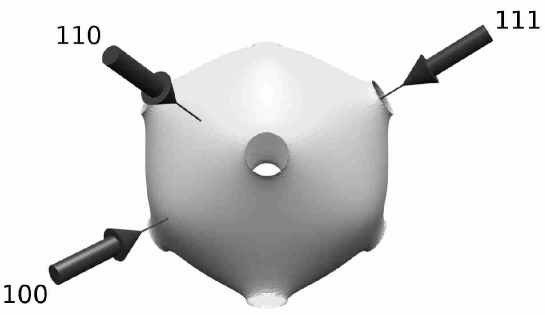
The FS (Conductance of a tunnel point-contact of noble metals in the presence of a single defect) has the BCC symmetry. It basically looks like a sphere with 8 ’necks’ positioned at the 8 vertices of a cube (Fig. 1). The central part of the surface (‘belly’) has a positive curvature while the ends near the Brillouin zone boundary (‘necks’) have negative curvature. The size of the ’necks’ and the curvature of the spherical areas are slightly different for each noble metal. In the regions of ’necks’ there are the inflection lines, at which the curvature
In Eq. (Conductance of a tunnel point-contact of noble metals in the presence of a single defect) for the FS, the , and directions correspond to a [100] direction, and the interface plane is therefore a (100) crystal plane. To align the plane with a (110) plane, the FS is rotated by along the or axis. For the (111) orientation, the total rotation consists of a rotation of along the -axis, followed by a rotation of arcsin along the or axis.
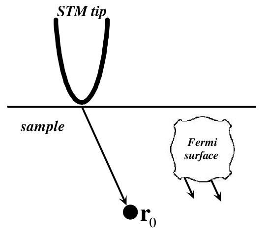
A direct way to find solutions of Eq. (4) numerically for a certain position of the defect and calculate (2) is not most suitable. Instead, the result that corresponds to the direction of the electron velocity along the direction from the contact to the defect can be used. We start with a point on the FS, calculate the value of for every point in the real space, and then repeat this for all points on the FS. Next, it is easy to perform the summation over all points on the FS, in which to obtain the conductance. This idea is shown schematically in Fig. 1.
Strictly speaking, the asymptotic Eq. (1) is correct at However, as it was shown in Ref. Avotina2 from a comparison of the exact result for the ellipsoidal FS with asymptotic expression (1), Eq. (1) describes the conductance qualitatively correctly for and distances of a few The other point is that at the inflection lines, which defines the classically unacceptable regions, the curvature As it was shown in Ref. Avotina2 , for such directions of the vector the amplitude of the conductance oscillations increases remains finite. Below we restrict ourselves to the condition and do not approach the inflection lines to a distance for which the second term in the Eq. (1) becomes of the order of unity.
We present the result of computations for three different crystallographic orientations (Fig. 2). The conductance as a function of the contact position for a defect in a noble metal at various depths are plotted in Figs. 3-5 for the (100), (110) and (111) lattice orientations respectively. For each of the lattice orientations, the graphs have the symmetries of that particular orientation of the FS. In all figures ’dead’ regions, in which there are no conductance oscillations, can be seen. These regions originate from the ’necks’ of the FS and their edges are defined by the inflection lines. In our plots the edges are abrupt. In reality there is a smooth change from a maximum to a zero of amplitude of the oscillations in the ’dead’ regions. This change can not be described by Eq.(1), and a numerical solution of the Schrödinger equation with energy-momentum relation (Conductance of a tunnel point-contact of noble metals in the presence of a single defect) must be used. However, the problem becomes much more complicated, while it does not give any additional physical information. The rings of high amplitude conductance oscillations have already been reported in experiments on Ag and Cu (111) surfaces Quaas .
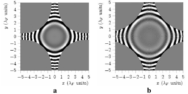
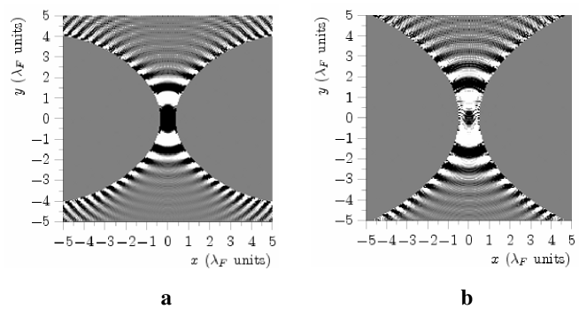
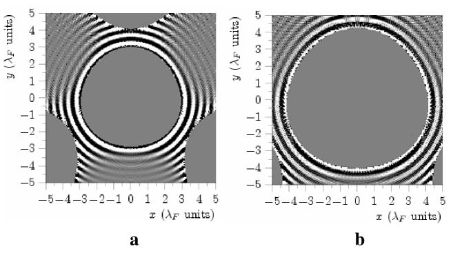
From Figs. 3-5 it can be seen that the interference pattern of the conductance oscillations, in particular the size and appearance of ’dead’ regions depend on the depth of the defect. These characteristics of the part of the conductance related to the scattering by the defect contains the information about the position of the defect. For all orientations of the metal surface the defect position in the plane of the surface corresponds to a center of symmetry. The depth can be found in the following way: The orientation of the ’neck’ axes defines the axes of the cones, in which there are no scattered electrons. Vertexes of the cones coincide with the defect. If the contact is situated in a point, which belong to a sectional plane of the cones by a surface plane, the conductance of the contact is equal to its value without the defect (we called these ’dead’ regions). A rough estimation of the defect depth can be obtain, if we use the approximation of a cone of revolution with an opening angle For example, in Fig.5 the radius of the central ’dead’ region is defined by the equality ,() Quaas . Using a fiting of experimental results with theoretical calculations in the framework our method enables one to find the depth of the defect below metal surface more exactly.
Thus, we have demonstrated the possibility of calculations of anisotropic conductance oscillation caused by electron scattering by the defect in noble metals. The developed algorithm of calculations can be used for any parametrically given FS. We have shown that the analysis of interference patterns makes it possible to find the position of the defect below metal surface.
This work was partly supported by Fundamental Research State Fund of Ukraine (project 25.2/122).
References
- (1) Ye. S. Avotina, Yu. A. Kolesnichenko, A.F. Otte, and J.M. Ruitenbeek, Phys. Rev. B, 74, 085411 (2006).
- (2) M. F. Crommie, C. P. Lutz, and D. M. Eigler, Science 262, 218 (1993).
- (3) O. Yu. Kolesnychenko, R. de Kort, M. I. Katsnelson, A. I. Lichtenstein and H. van Kempen, Nature 415, 507 (2002).
- (4) N. Knorr, H. Brune, M. Epple, A. Hirstein. M.A. Schneider, and K. Kern, Phys. Rev., 65, 115420 (2002).
- (5) L. Bürgi, N. Knorr, H. Brune, M.A. Schneider, K. Kern Appl. Phys. A 75, 141 (2002).
- (6) M. Schmid, W. Hebenstreit, P. Varga and S. Crampin, Phys. Rev. Lett., 76, 2298 (1996).
- (7) N. Quaas, PhD thesis, Göttingen University (2003).
- (8) N. Quaas, M. Wenderoth, A. Weismann, R.G. Ulbrich and K. Schönhammer, Phys. Rev. B 69, 201103(R) (2004).
- (9) P.T. Sprunger, L. Petersen, E.W. Plummer, E. Lagsgaard, F. Besenbacher, Science 275, 1764 (1997).
- (10) Ph. Hofmann, B.G. Briner, M. Doering, H.-P. Rust, E.W. Plum-mer, and A.M. Bradshaw, Phys. Rev. Lett. 79, 265 (1997).
- (11) L. Petersen, P. Laitenberger, E. Lægsgaard, and F. Besenbacher, Phys. Rev. B 58, 7361 (1998).
- (12) Ye. S. Avotina, Yu. A. Kolesnichenko, A.N. Omelyanchouk, A.F. Otte, and J.M. Ruitenbeek, Phys. Rev. B 71, 115430 (2005).
- (13) Ye. S. Avotina, Yu. A. Kolesnichenko, A.F. Otte, and J.M. Ruitenbeek, Phys. Rev. B 75, 125411 (2007).
- (14) I. O. Kulik, Yu. N. Mitsai, and A. N. Omelyanchouk, Zh. Exp. Teor. Fiz., 63, 1051 (1974).
- (15) A.M. Kosevich, Fiz. Nizk. Temp., 11, 1106 (1985) [Sov. J. Low Temp. Phys., 11, 611 (1985)].
- (16) I.M. Lifshits, M.Ya. Azbel’, and M.I. Kaganov, ”Electron theory of metals”, New York, Colsultants Bureau (1973).
- (17) G. Korn, T.Korn, ”Mathematical Handbook”, McGraw-Hill Company (1968).
- (18) Arthur P. Cracknell, The Fermi surfaces of metals: a description of the Fermi surfaces of the metallic elements, Taylor and Francis, London (1971).