Low noise cryogenic system for measurement of the Casimir energy in rigid cavities
Abstract
We report on preliminary results on the measurements of variations of the Casimir energy in rigid cavities through its influence on the superconducting transition of in-cavity aluminium (Al) thin films. After a description of the experimental apparatus we report on a measurement in presence of thermal photons, discussing its implications for the zero-point photons case. Finally, we show preliminary results for the zero-point case.
1 Introduction
In spite of great theoretical and experimental advances [1, 2], the Casimir effect still faces important unsolved questions. In Gravitation and Cosmology the problem of reconciling the vacuum energy density and its interaction with the gravitational field, known as the cosmological constant problem [3, 4], remains unsolved. In flat space-time, theoretical disagreements still remain on the dependence of the Casimir energy (and force) on the geometrical shape of the bodies and on the possibility that some geometries exhibit positive energy and repulsive force [1]. All experiments performed so far have been addressed to measure the forces between (two) separate bodies, not directly the (variation of) energy in a rigid body. Apart from the fundamental interest of a direct measurement of the energy, the use of rigid cavities could make it easier to test different shapes. The interest is not only theoretical: repulsive forces might build a bridge between the Casimir effect and nanotechnology. On this basis, we recently proposed the experiment Aladin2, to measure the variation of Casimir energy in a rigid cavity, occurring when a thin metallic film, constituting one of the plates of the cavity (the other plate being made of a normal metal) becomes superconducting [5]. The experiment is made possible by the observation that, under suitable conditions, the variation of vacuum energy in the transition (due to the change in the film reflectivity) can be comparable with the condensation energy of the superconducting film, and therefore it may sensibly affect the transition itself [5, 6]. In particular, the parallel critical field required to destroy the superconductivity of the film can be remarkably different from the critical field of a bare film so that, to prove this effect, the experiment measures the difference in the values of for a film which is part of a Casimir cavity with respect to an equal but bare film. The magnitude of the effect depends also on the roughness of the plates and on their conductivity, and hence, in principle, our method might be used to probe the dependence of the Casimir effect on these factors, which are currently being investigated experimentally. We remark that our approach, being based on rigid cavities, could be easily extended to measure the energy of different shapes, like for example granular superconductors. Finally we notice that the scheme of our experiment arose as a solution to the problem of modulating the Casimir energy in a rigid cavity [7], while introducing in the system the minimal amount of energy. This goal is part of a more speculative project, aimed at verifying whether or not Casimir energy gravitates, by weighing a Casimir apparatus whose energy is modulated in time [7].
2 Expected signal
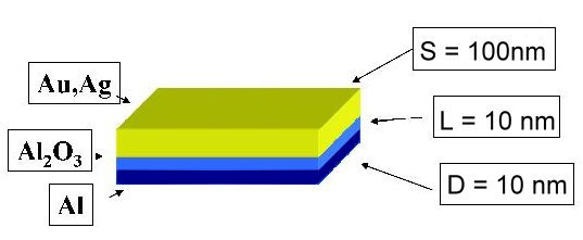
The Casimir cavity, shown in Fig. 1, is composed of a thin Al superconducting layer of thickness , an intermediate dielectric thin layer (Al2O3) of thickness and a third thick metallic layer made of gold (Au) or silver (Ag). (See below for more details).
The expected effect is shown in Fig. 2 where the shift of the reduced critical temperature is plotted against the critical field ; is the zero-field transition temperature. The upper curve is for a bare superconducting thin film while the lower curve is for the Casimir cavity. For a bare film with , as it is our case, the critical field follows the well known equation [8]:
| (1) |
which neglects the effect of nucleation, which applies to a very thin film. Here, is the penetration depth and is the bulk zero temperature critical field. On inverting Eq. (1), one obtains a parabolic dependence of on , corresponding to the upper curve of Fig. 2.
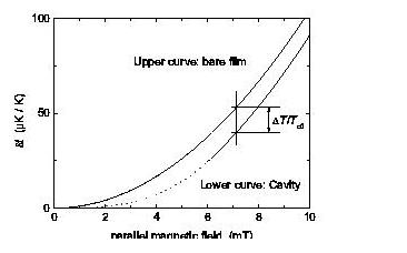
In a cavity the dependence is expected to differ from the bare film case in the region , corresponding to low applied fields. As shown in Fig. 2 the expected difference in the transition temperature for low applied fields is in the range of a few K. (for higher values of the field, not shown in the plot, the two curves approach each other) [5, 6, 9]. In the region of very small applied fields, a deviation from the parabolic curve is expected by continuity arguments (dashed line in Fig. 2); in this latter region the change in free energy becomes comparable with the condensation energy and no perturbative calculation can be done. The choice of the material is crucial, and a compromise is usually required to encompass various needs. On the one hand, low materials (low condensation energy) are preferable because their transition is more perturbed by vacuum energy effects [6]. On the other hand, the longer cooling times typically required when working with (very) low materials could make it difficult to increase the statistics. In this first experiment Al has been chosen has a good compromise. Another important parameter is the plasma frequency of the normal plate; larger values of imply a larger conductivity and ensure a better confinement of the photons within the cavity. It was shown in Ref. [6] that a very good material could be Be ( eV), but difficulties in obtaining cavities with this material led us to use Au ( eV) or Ag ( eV), resulting in a loss of approximatively a factor of 2 in the expected signal [6]. The values of other electrical parameters, such as the electrons mean free paths both in the normal metal and in the superconductor, do not affect significantly the expected signal [6]. While the signal does not depend on the area of the plates, the optimal thickness of the superconducting metal turns out to be of a few nanometers. Numerical calculations show that the variation of vacuum energy in the transition has the following dependence on the gap L:
| (2) |
where and nm. As we see, as soon as becomes smaller than , approaches a finite value and therefore, once is in the region of few nanometers, no substantial gain can be obtained by using smaller gaps. It can be shown that the signal is practically independent of the dielectric material, and we chose the Al native oxide Al2O3. In order to overcome spurious effects due to different alignment of the cavity and the bare film with respect to , the cavity and the bare film are placed on the same chip.
3 Sample preparation, cryogenic apparatus and measurement method
The films and cavities, made by IPHT (Institute for Photonic Technology - Jena - Germany), are obtained by depositing the Al on the whole wafer (silicon, 3 inch diameter). The only difference between the bare thin film and the cavity is the presence of a metallic layer above the dielectric layer for the cavity. Finally the chip is cut in samples that include, within a distance of less than a mm, several films and cavities. Considering our parameters, as we reported elsewhere [9, 11], the applied magnetic field must be very homogeneous, to within over the distance between the cavity and the film (mm). This requirement has been fulfilled by a home-made coil system composed by a main coil and two lateral correction coils. The alignement of the field and sample is performed by mounting rigidly the sample holder and the coil system. If is the angle between the magnetic field and the sample, following [8], for small angle , a perpendicular component of the field adds a linear term in the dependence , resulting approximately in
| (3) |
Since the film and the cavity are deposited at close distance on the same chip, and since the magnetic field is very homogeneus, possible differences in the values of and between the film and cavity can be neglected and therefore a non-vanishing just yields a common additive term which does not affect the differential measurement.
We used films with different areas, ranging from about m2 to m2, to verify that the effect does not depend on the area. Inspection of the samples with the atomic force microscope showed that the actual thicknesses of the Al layer and the of the oxide gap are of 14 nm and 6 nm respectively. The roughness is about 1 nm for both. Measurements of different samples do not show any significant difference. The cryogenic system is based on the HelioxVL 3He commercial cryostat from Oxford Instruments, reaching a base temperature of mK, inserted in a home-made dewar equipped with magnetic screening, to isolate the sample from undesired environmental fields. The usual ferrite-filters at K and 1K-pot levels and a cascade of two isolation copper-powder filters [10] at the level of the 1K-pot and the 3He-pot guarantee efficient EM screening.
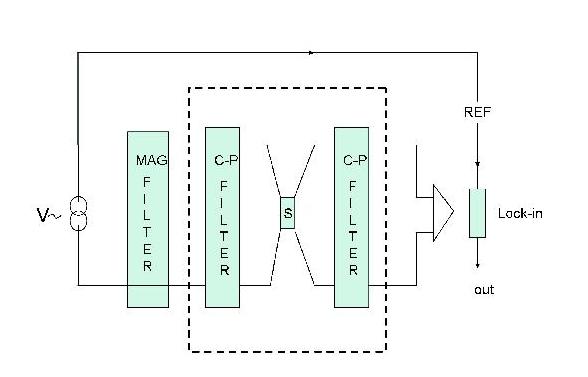
The measurement method for film and cavity resistances is a standard four-wire measurement, as shown in Fig. 3. The temperature is measured by a Cernox CX-1070-BR as part of a Wheatstone bridge. Both measurements are done with lock-in technique. The actual measurement of is performed by fixing the external field, driving the temperature from low to high and measuring and ( is time) at the sample during the transition. The cool down is always performed in zero magnetic field to avoid magnetic flux trapping. Each single transition measurement takes approximately 20 minutes. is finally recovered to evaluate the shift with respect to zero field case. The Al resistivity ratio of the cavities and films analyzed in the present work is KK, compatible with values quoted in the literature, corresponding to a mean free path of about 15 nm [12]. The samples resistances vary from to . The transition temperature at zero field, , is taken at the maximum of the derivative of and used as the normalization factor in . In order to minimize the error in the measurement, is obtained as the difference of temperature not just at a given point on the transitions with and without applied field (i.e. for a given resistance ), but as the average of the differences for all points of the transition (i.e. for all values of ):
| (4) |
The average is taken over the points with , where is the resistance in the normal state.
4 Measurement in the presence of thermal photons
In order to test the cavity efficiency in removing photons affecting the transition, we performed a first measurement in the presence of room-temperature thermal photons. This has been done by removing the cascade of copper powder filters and allowing the external rf and microwave photons enter the vacuum chamber. As pointed out in [6], the important region of frequencies contributing to our effect is around a few times . In the absence of a detailed theory, as a first guess one can imagine that the presence of extra thermal photons from the environment at temperature K gives rise to a temperature shift that is larger than the previous by a factor equal to the ratio between the black-body densities and of electromagnetic energy at frequency , at temperatures and respectively. Upon taking, to be definite, , we obtain
| (5) |
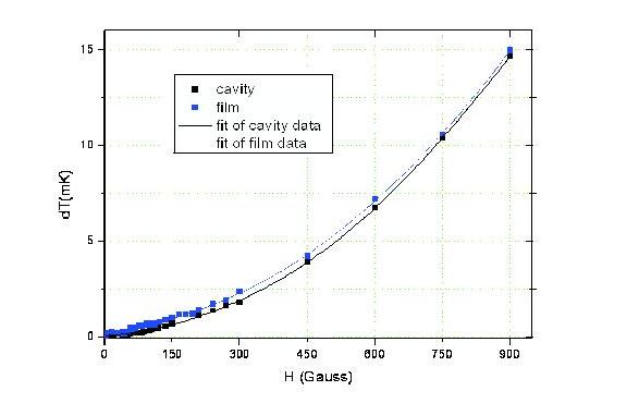
From this estimate we expect that this measurement (which, apart from the filters, is the same as the one described earlier), should produce a signal similar to the one described in Fig. 2, with increased by a factor of some tens. As shown in Fig. 4, this is what we indeed found in our measurements: the curves relative to the bare film and the cavity, for low , are separated by a gap which reaches a maximum of about K. We point out that, although it must be considered as a rough estimate, this measurement suggests a value of in the final experiment close to the most conservative expectation of K (or even less).
5 First results in the measurement of Casimir energy variations
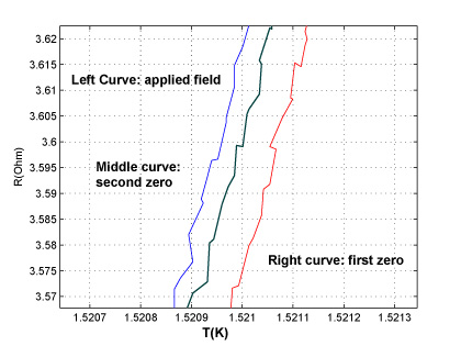
In the presence of copper powder filters, the major sources of noise is the electronic noise at the read-out amplifier. This noise has a “fast” component (with time scale of one second) that determines a statistical error of a few K, and a slow thermal drift (linear in time, about K per hour) that produces a proportional to the time elapsed between two measurements. To correct for the thermal drift, at equal time intervals before and after each measurement with applied field, we perform two measurements in zero field, and then we take for the average of the two ’s. We performed the measurement on three different samples, without finding significant differences. An example of such a measurement is shown in Fig. 5: the intermediate curve and the right curve were taken in zero field, while the left curve is with an applied field of mT. It should be noted that the shifts in temperature for the three curves are only a few tens K. This procedure is repeated for all applied fields.
The data for a typical bare film are reported in Fig. 6. The parallel field is applied in opposite directions to rule out possible hysteresis. We find that the theoretical parabolic dependence of on the applied field is recovered for fields as low as a few mT, corresponding to changes of critical temperature of about K. The sensitivity has been roughtly estimated to be about K by comparing several measurements of under the same conditions, performed at some days of distances.
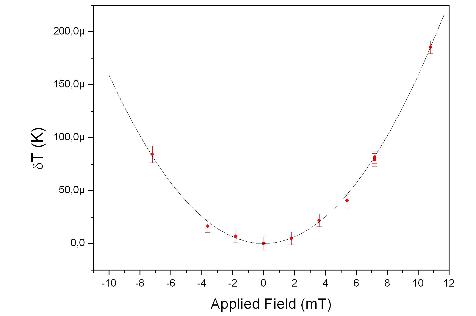
It is important to stress that the solid line was obtained by fitting high-field measurements (data not shown), which are less affected by the possible presence of EM noise or field-film misalignment. The good agreement of the solid line with the low-field measurements indicates that there are no unexpected sources of noise in the low field region.
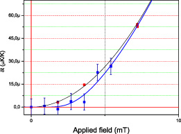
An example of a complete measurement, for one of our samples, is reported in Fig. 7. Other samples do not show significant differences at the present level of sensitivity. The upper curve is the same bare-film parabola of Fig. 6, while the lower curve is a fit on the cavity data. To help reading the figure, the bare film data are reported without errors. The cavity curve lies below the bare film curve, and it shows a non-parabolic behavior, in qualitative agreement with theoretical expectations. Moreover the maximum displacement between the two curves, of about K, is of the expected magnitude. However, it is also comparable with the present sensitivity and therefore the result of these measurements, while encouraging, is far from being conclusive. In addition to this, the two curves appear to merge much faster than expected theoretically, and the reason for this is presently not clear.
In order to increase the sensitivity, a new cryogenic apparatus is being built, allowing to reach lower temperatures (about 20 mK) and to use softer superconductors. We expect that the signal-to-noise ratio will improve, as discussed in section 2, to a sufficient extent to definitively confirm or disprove the foreseen effect.
References
References
- [1] Bordag M, Mohideen U and Mostepanenko V M 2001 Phys. Rep. 353 1
- [2] For most recent experiments: Castillo-Garza R, Chang C C, Jimenez D, Klimchitskaya G L, Mostepanenko V M and Mohideen U 2007 Phys. Rev. A 75062114; Bressi G, Carugno G, Onofrio R and Ruoso G 2002 Phys. Rev. Lett 88 041804 ; Decca R S, López D, Fischbach E, Klimchitskaya G L and Krause D E 2007 Phys. Rev. D 75, 077101; Iannuzzi D, Lisanti M and Capasso F 2004 Proc. Nat. Ac. Sci. USA 101, 4019
- [3] Weinberg S 1989 Rev. Mod. Phys. 61 1
- [4] Ishak M 2007 Found. Phys. 37 1470
- [5] Bimonte G, Calloni E, Esposito G, Milano L and Rosa L 2005 Phys. Rev. Lett. 94, 180402
- [6] Bimonte G, Calloni E, Esposito G and Rosa L 2005 Nucl. Phys. B 726 441
- [7] Calloni E, Di Fiore L, Esposito G, Milano L and Rosa L 2002 Phys. Lett. A 297 328 (2002).
- [8] Tinkam M 1975 Introduction to Superconductivity (Mc Graw-Hill, New York)
- [9] Bimonte G, Born D, Calloni E, Esposito G, Hübner U, Il’ichev E, Rosa L, Tafuri F, Scaldaferri O and Vaglio R 2007 Nucl. Instrum. Meth. A 572 515
- [10] Martinis J M, Devoret M H and Clarke J 1987 Phys. Rev. B 35 4682
- [11] Bimonte G, Born D, Calloni E, Esposito G, Hübner U, Il’ichev E, Rosa L, Tafuri F, Scaldaferri O and Vaglio R 2006 J. Phys. A 39 6153
- [12] Van Son P C, Romiijn J, Klapwijk T M and Mooij J E 1984 Phys. Rev. B 29 1503