Microwave band on-chip coil technique
for single electron spin resonance in a quantum dot
Abstract
Microwave band on-chip microcoils are developed for the application to single electron spin resonance measurement with a single quantum dot. Basic properties such as characteristic impedance and electromagnetic field distribution are examined for various coil designs by means of experiment and simulation. The combined setup operates relevantly in the experiment at dilution temperature. The frequency responses of the return loss and Coulomb blockade current are examined. Capacitive coupling between a coil and a quantum dot causes photon assisted tunneling, whose signal can greatly overlap the electron spin resonance signal. To suppress the photon assisted tunneling effect, a technique for compensating for the microwave electric field is developed. Good performance of this technique is confirmed from measurement of Coulomb blockade oscillations.
I Introduction
Electronic spin confined to quantum dots (QDs) is a robust quantum number Petta et al. (2005) and is therefore regarded as a good candidate for forming a quantum bit in quantum information processing Hatano et al. (2004, 2005). Electron spin resonance (ESR) is a powerful tool for achieving coherent spin rotation in the qubit operation and is realized by applying a microwave (MW) magnetic field perpendicular to a static Zeeman field. ESR is usually achieved using a MW cavity. However, this technique is unsuitable for QDs since the MW cavity usually raises the temperature of the spin qubit to an unacceptable level because it transmits direct radiation from room temperature. One solution is to use a low temperature cavity. Then we deal with this heating problem by using an on-chip MW coil Kodera et al. (2004, 2005); van der Wiel et al. (2006) to which the MW is transmitted through coaxial cables to avoid direct room temperature radiation.
Single spin ESR was recently demonstrated using a spin blockade readout technique for a double QD system with an on-chip coil structure Koppens et al. (2006). Unlike a single dot, the spin blockade charge readout scheme is efficient for realizing a low Zeeman field, in that it allows the on-chip coil to be operated at a low frequency (100 MHz). Here we aim to extend the frequency band to the gigahertz level, so a higher Zeeman field can be used that has much higher energy of 1 K (Refs. Koppens et al. (2006) and Hanson et al. (2003)) than the electron temperature.
We set a static magnetic field to produce Zeeman splitting for an electron in a QD and apply MW. If the frequency matches the resonance condition, the MW magnetic field flips the spin to the excited state, which is positioned in the reservoir transport window. The electron can then exit the QD generating a finite current. However, capacitive coupling between a coil and a QD concurrently causes photon assisted tunneling (PAT)Kouwenhoven et al. (1994); van der Wiel et al. (2002, 2003), which also excites the electron out of the QD. This PAT process smears out the ESR signal. Therefore, it is crucial to minimize the MW electric field by optimizing the on-chip MW coil to suppress the PAT effect. We perform this on-chip coil optimizations after numerical simulation and experimental test.
This paper is organized as follows. Section II describes on-chip coil designs. The coil is connected to an on-chip high frequency transmission line to minimize insertion loss. Simulation results for several coil-waveguide structures are presented and compared. Transport measurements obtained through QD devices under MW excitation provided by the integrated coil are presented in Sec. III. We check the return loss, which affects the QD transport regarded as the PAT process. Koppens et al. Koppens et al. (2006) previously developed a technique for canceling the PAT effect by using antiphase radio wave irradiation from a nearby antenna for lower frequencies. They attenuated and delayed the cancelation signal to minimize the MW electric field. The observed PAT signal was suppressed periodically with respect to frequency. We modified their technique for the higher frequency band using a variable phase shifter instead of a delay cable for tunable frequency. In Sec. IV, we analyze the experimental data and calculate the amplitude of the MW electric field. We compare them with the help of numerical simulation to finally estimate the MW magnetic field.
II Design of on-chip coil
II.1 Transmission line
Microstrip
Coplanar strip (CPS)
Coplanar wave guide (CPW)
| Lines | Metalwidth () | Gap () |
|---|---|---|
| Microstrip | 360 | … |
| Coplanar wave guide(CPW) | 14 | 10 |
| Coplanar strip(CPS) | 100 | 10 |
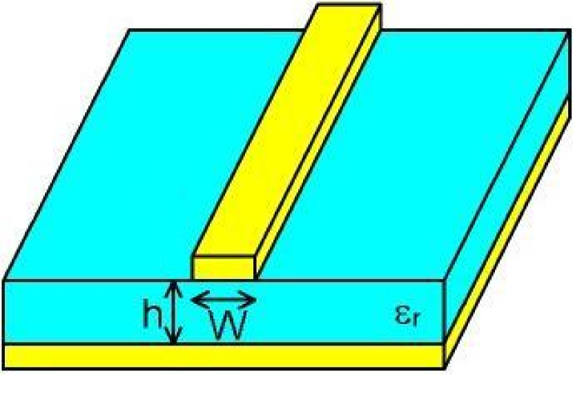
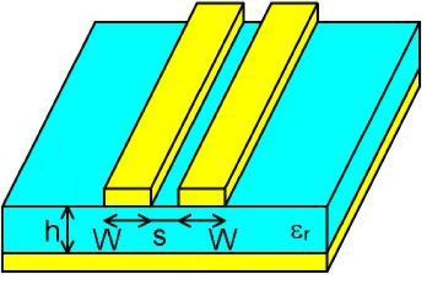
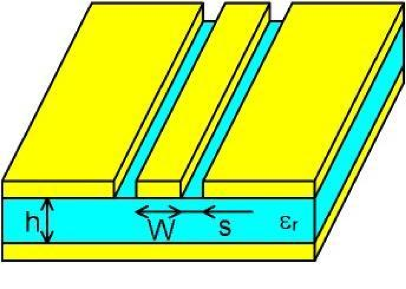
In this section, we describe the design of our on-chip coil. The emerging problem in the MW band is heating. The metal becomes more resistive in proportion to the square root of the frequency because of the skin effect. We can deposit a several times thicker (approximately micrometer) metallic coil using a technique of photolithography rather than electron beam lithography. To obtain an ideal structure in terms of characteristic impedance, it is better to properly make for the metal thicker than 1 . The typical skin depth decreases in inverse proportion to the square root of the frequency and is typically half a micrometer at 10 GHz. The line becomes more resistive than the simulation result for the metal thinner than 1 . Thermal conductivity is larger for the thicker metal and thus allows the application of a MW signal with the larger current. The coil metal is approximately micrometer wide.
The approximately micrometer wide coil is placed solely just around the QD. On-chip transmission lines are used to deliver a MW to the coil. The characteristic impedance of these lines is adjusted to that of factory made coaxial cables (i.e., = 50 ). Characteristic impedance is a function of the line geometry. According to textbooks such as Ref. Okada (2004), the formulas of as a function of the dimensions for typical planar transmission lines are shown in Fig. 1. The parameters are the metal width and gap. Their typical values are given in Table 1 for = 50 . The dielectric constant of the host material, GaAs, , is used for the calculation. The microstrip shown in Fig. 1 is the simplest for the MW transmission line. However, we did not employ it because it requires a width of as much as 360 . Koppens et al. Koppens et al. (2006) previously used a coplanar strip (CPS) transmission line for the ESR experiment. We used a coplanar waveguide (CPW) structure instead because the necessary surface area is smaller than CPS for an identical gap.
Another factor related to the impedance is the reflection property. When the coil impedance is connected to a transmission line with characteristic impedance , the MW is reflected at the input port of the coil. The reflection coefficient is . In the present MW range, many parameters such as line curvature, resistivity, and metal thickness change the impedance. Bonding wire produces an additional impedance, which cannot be calculated easily. So, in this paper, we only examine if PAT occurs effectively (ineffectively) at the local minimum (maximum) reflection frequency (see Sec. III).
II.2 Numerical calculations
| Magnetic field (mT) | Electric field (mV/) | |
|---|---|---|
| Single | 1.9 | 21 |
| Spiral | 0.5 | 4 |
| Resonator | 1.9 | 11 |
(a)
(b)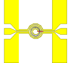
(c)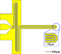
(a)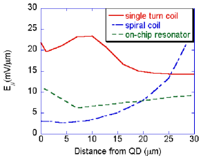 (b)
(b)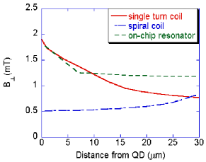
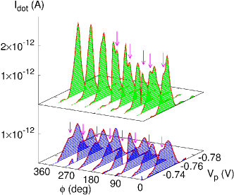
We start with a simple design, which involves winding a CPW line to form a single turn coil [Fig. 2(a)]. When a CPW is bent at 180∘, a ground plane always remains between the input and output lines. This plate can be removed if we maintain the same pitch for the signal lines as that for the ground plane Kanaya et al. (2004). A QD is placed in the gap between the input and output lines. A similar design was previously tested using a CPS at a lower frequency Koppens et al. (2006). The simulations for the MW electric and magnetic fields are performed for our designs at 20 GHz using commercial software IE3D (Table 2). Figure 3 shows the obtained in-plane electric field and perpendicular magnetic field profiles near the QD location. The input port is connected to the MW source and the output is grounded. The single line coil induces a stronger electrical field than expected, as discussed below. To concentrate the current density in the coil near the QD is a straightforward way to increase the magnetic field. This can be done by making the CPW line narrower toward the QD. However, in reality it also strongly increases the electric field in our simulation.
Concerning the development of on-chip MW structures, there are already many studies performed on the on-chip spiral coil structureBoero et al. (2003). We followed these studies and developed the on-chip spiral coil shown in Fig. 2(b). We calculated the basic properties of our on-chip spiral coil and plotted them in Fig. 3. We adjusted the coil diameter to maximize the magnetic field. Compared with the single line structure, the electric field is greatly reduced but the magnetic field is small. Then we judge the spiral coil is not practical. When we calculate the ratio of the magnetic field to the electric field, we found that effectiveness is the same as that for the resonator type (see below). Note that regarding the field homogeneity, the on-chip spiral coil can produce the most homogeneous field.
To minimize the electric field, we consider the on-chip resonator Blais et al. (2004); Wallraff et al. (2004) shown in Fig. 2(c), which consists of a long CPW line of length with one port grounded. A standing wave with a voltage node at the ground port is forced along the line. The structure is similar to that of the single turn coil; however, the single turn coil has no resonance mode simply because the length is too short. If the coil has a resonance mode, it works more effectively at the resonant frequency. We calculate the effective wavelength on the surface of GaAs to derive the resonance condition. Using the effective dielectric constant , is calculated as , where is the wavelength in a vacuum.
There are voltage and current nodes at different locations ( phase shift). For with an odd integer , an antinode appears in the voltage at the QD location [at the center of the circle in Fig. 2(c)]. Under this condition, we expect a large electric field and a small magnetic field. Then is about 3 mm to satisfy the condition at 20 GHz, and therefore we insert a meander lineKanaya et al. (2004) to fit the line into a sample with a size of 21.6 mm2. When is an even integer, a node and an antinode appear in the voltage and the current, respectively. Therefore, the maximum magnetic field is expected at the QD location. The simulation results are plotted in Fig. 3. The data are obtained at 20 GHz both for comparison with the single turn coil and for the worst case calculation for ESR with a larger electric field. This resonator design clearly provides better characteristics for ESR than other designs and the strongest magnetic field.
III Experiments
III.1 Experimental setup
(a)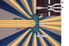 (b)
(b)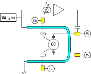
We used our integrated on-chip coil and QD devices in a dilution refrigerator to characterize the MW performance. Two semirigid coaxial cables were fitted to supply the sample with MWs. These cables transmit signals of up to 46 GHz. The heat load was measured at 20 W per cable, which raised the base temperature to 40 mK. A gold CPW on an alumina substrate was connected to the semirigid coaxial cable via factory made glass beads. The high frequency port of the on-chip coil was connected to the alumina CPW with 1 mm long bonding wires.
Images of the device and a circuit sketch are shown in Fig. 4. We used a Canadian design Ciorga et al. (2000) to make a lateral QD holding just a single electron and supplied a MW to the on-chip coil. We estimate that a 4 dBm input power produces 4 mA under impedance matching condition. At this power level the dilution refrigerator temperature increased to 300 mK.
III.2 Reflection property and coulomb peaks
(a)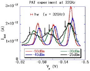 (b)
(b)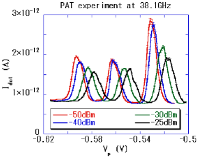
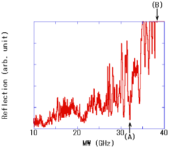
In this section, we characterize the reflection coefficient of the coil circuit. For the first experiment we used a single turn coil similar to the design shown in Fig. 2(a). With this coil, we expect a stronger PAT effect than for the resonator-type sample. When we applied a MW to the sample through the transmission line, part of the MW did not transmit. The reflection coefficient was measured using a network analyzer and a standing wave ratio bridge. The frequency dependence of the absolute value of is shown in Fig. 5, which we measured with an Anritsu autotester 560-98VF50A. There is a frequency region where the reflection is small. We can expect high efficiency for the MW performance at around this frequency region. Figure 6 shows the measured Coulomb peaks at two characteristic frequencies: (a) close to the local minimum (32 GHz) and (b) local maximum (38 GHz) of the reflection. The power dependence of the QD Coulomb blockade spectrum is shown in Fig. 6.
Figure 6(a) shows side peaks (arrows) caused by PAT and the peaks become broad with increasing MW power. On the other hand, Fig. 6(b) shows the principal peaks just shifting with increasing MW power for the frequency at the antiresonance value of 38 GHz. The MW is not transmitted into the sample. Then Joule heating along the coaxial line causes the peak to drift. The MW at the resonance frequency propagates to the on-chip coil and generates the PAT signal. These results provide a guideline about the MW frequency where we should work for the ESR measurement. Nevertheless, the PAT process still presents a problem. The next step is to focus on applying a magnetic field and reducing the electric field in order to remove the PAT signal.
III.3 PAT compensation
To detect ESR, it is desirable to attenuate the PAT process. We developed the compensation circuit Koppens et al. (2006) to operate in the more active way and at the much higher frequency. We used the resonator-type on-chip coil, as shown in Fig. 4. We split the MW signal and used a block attenuator to adjust the compensation level. After adjusting the phase with a mechanical phase shifter (Waka Manufacturing Co., Ltd.) to maximize the compensation level, we launched the MW into one of the side gates through a bias tee A3N1025 (Anritsu Corp).
The compensation results are shown in Fig. 7. The MW frequency is 40 GHz. If the compensation level matches the electric field provided by the on-chip coil, the side peak (arrow) is suppressed and the main peak is increased. This is the case shown in the upper panel of Fig. 7. The main peak becomes sharpest when the phase is best adjusted. When the compensation level does not match, the compensation works poorly as seen in the lower panel of Fig. 7. Under the best compensation condition, there is only a standing magnetic field, which is a good regime for detecting ESR. The active compensation technique holds for any frequencies, using a continuous phase shifter. Actually we obtained similar results at other frequencies. When the phase matches and compensation works well, we can apply almost 0 dBm at the sample edge.
IV DISCUSSION
(a)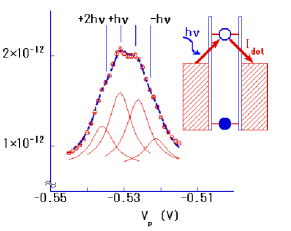 (b)
(b)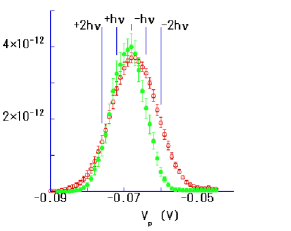
From both the simulation and experiment, we confirmed that the resonator-type coil is a better choice. To characterize the coil performance on the QD more quantitatively, we now analyze the effect of MW modulation on the Coulomb blockade peaks in Figs. 6 and 7. The change in the peak arises from the PAT process such that electrons in the QD are injected (ejected) from (to) the reservoirs absorbing (emitting) photons Kouwenhoven et al. (1994); van der Wiel et al. (2002, 2003). Due to the PAT process there appear several small peaks/shoulders (arrows) with the spacing given by the photon energy . Following the standard PAT model, we define an oscillating potential at the QD. A voltage drop across a tunnel barrier modifies the tunnel rate through the barrier as Tien and Gordon (1963)
Here . and are the tunnel rates at energy with and without MW irradiation, respectively. ’s are Bessel functions of the first kind. We define . We apply this equation to the simplest case of a nondegenerate single QD level. We focus on the situation that the electron number changes from to (see the inset in Fig. 8). We take into account the charge balance between the QD and source-drain and the electron number conservation law (the so-called master equations) and calculate the net current as
| (1) |
, , , and are the energy level of dot, bare tunnel rate to the left (right) contact, gate voltage, and source-drain bias voltage, respectively. is the Fermi-Dirac distribution function and coefficients and are the lever arms measured by nonlinear Coulomb blockade spectroscopy Kouwenhoven et al. (1997). gives a peak at with amplitude proportional to .
The electric field produced by the coils can be estimated by fitting the line shape of the Coulomb blockade peak to Eq. 1. We approximate by a Lorentzian function because the data contain many kinds of experimental errors and take into account up to the two-photon process. For the single turn coil, we analyzed the data at 32 GHz with -30 dBm input (4.5 mV at the sample edge) in Fig. 6 because the data show clear PAT structures. One of the fitting results is shown in Fig. 8(a). The fitting parameters have some ambiguity, but we finally estimated the averaged voltage drop of 150 V using the value of . The distance crossing the tunnel barrier was estimated to be 300 nm yielding an electric field of 0.5 mV/.
For the resonator type, we measured the MW modulation under the similar condition (at 28 GHz with -30 dBm input) for comparison in Fig. 8(b). We tried but the PAT structure was not well resolved. We could only estimate from the change of the main peak to be proportional to and the electric field of 0.17 mV/ at 28 GHz with -30 dBm input. The MW modulation at 40GHz shown in Fig. 7 was more easily analyzed. In the lower panel, we estimated 0.6 mV/ with -20 dBm input by fitting. Then we estimated that the electric field at 40 GHz would be 0.2 mV/ with -30 dBm input.
The single turn coil data show larger MW modulation than that for the resonator coil in both simulation and experiment. The simulation generally gives us a good guideline for designing the on-chip coil. The electric field experimentally evaluated is, however, several times larger than the simulation. Another problem is that the simulation for the resonator type predicts magnetic resonance at 40 GHz with zero electric field, whereas the experiment shows a finite electric field under the resonance condition. We consider that these problems come from the bonding wires for connecting the input and ground because they can produce an extra impedance and modulate the resonance mode. The misalignment between the MW lines and the QD also gives a larger electric field in the experiment than that in the simulation because the MW lines are symmetric around the gap where the QD is placed. The alignment precision is restricted by an optical mask aligner precision, which is a few micrometers for the high frequency lines.
To estimate the MW magnetic field, we compared the electric field for PAT data to the simulation and assumed that the ratio between the MW electric and magnetic fields is the same for the simulation. The estimated magnetic field is 0.4 g at -30 dBm. We used the ratio in the case that electric field is larger (see Sec. II.2) and thus this estimation is somewhat underestimation of MW magnetic field. Under the compensation condition described above, we can apply a 0 dBm input, and then the magnetic field will be 30 times larger or 1 mT. Note with standard cavity resonators, it is very difficult to produce such a high magnetic field. If electron factor is 0.35 Koppens et al. (2006), the spin flip time is 2.5 MHz, which is detectable level when the tunneling rate of Coulomb blockade peak is about 10 MHz (1pA current). We can expect to detect an ESR signal under these conditions.
V Conclusion
We reported designs for a MW band on-chip coil and experimental techniques for actual devices with QDs. We simulated three types of on-chip coil structure. The single turn coil pattern is the simplest but it produces the strongest MW electric field in our models. In accordance with conventional NMR and ESR studiesBoero et al. (2003), we designed an on-chip spiral coil. This produces a homogeneous magnetic field but a smaller amplitude. Another disadvantage for the spiral coil is that more microfabrication steps are necessary, and therefore the production yield will be low. Finally, the resonator-type pattern appeared more relevant than the others. We then fabricated samples with the resonator-type on-chip structure. We examined experimentally how strongly impedance matching affects the Coulomb blockade transport. With a low reflection coefficient, the current was modulated by a high frequency signal and there significantly appeared the PAT effect. It is clear that this PAT process overrides the electron spin resonance signal. To suppress the PAT effect and maximize the MW magnetic field, we developed a compensation technique available for the MW band. We demonstrated that the PAT side peak disappeared when the phase of the compensation signal was best adjusted. According to our calculation, we could predict that a sufficiently strong MW magnetic field is generated for the single ESR measurement with QD.
VI Acknowledgments
The authors thank W.G. van der Wiel for fruitful discussions. S.T. acknowledges financial supports from the Grant-in-Aid for Scientific Research A (No. 40302799), and B (No. 18340081), SORST Interacting Carrier Electronics, JST, and Special Coordination Funds for Promoting Science and Technology, MEXT.
References
- Petta et al. (2005) J. R. Petta, A. Johnson, J. Taylor, E. Laird, A. Yacoby, , M. Lukin, C. Marcus, M. P. Hanson, and A. Gossard, Science 309, 2180 (2005).
- Hatano et al. (2004) T. Hatano, M. Stopa, T. Yamaguchi, T. Ota, K. Yamada, and S. Tarucha, Phys. Rev. Lett. 93, 066806 (2004).
- Hatano et al. (2005) T. Hatano, M. Stopa, and S. Tarucha, Science 309, 205 (2005).
- Kodera et al. (2004) T. Kodera, W. G. van der Wiel, K. Ono, S. Sasaki, T. Fujisawa, and S. Tarucha, Physica E 22, 518 (2004).
- Kodera et al. (2005) T. Kodera, W. G. van der Wiel, T. Maruyama, Y. Hirayama, and S. Tarucha, in Realizing Controllable Quantum States, edited by H. Takayanagi and J. Nitta (World Scientific, Singapore, 2005), pp. 445–450.
- van der Wiel et al. (2006) W. van der Wiel, M. Stopa, T. Kodera, T. Hatano, and S. Tarucha, New J. Phys. 8, 28 (2006).
- Koppens et al. (2006) F. H. L. Koppens, C. Buizert, K. J. Tielrooij, I. T. Vink, K. C. Nowack, T. Meunier, L. P. Kouwenhoven, and L. M. K. Vandersypen, Nature 442, 766 (2006).
- Hanson et al. (2003) R. Hanson, B. Witkamp, L. M. K. Vandersypen, L. H. W. van Beveren, J. M. Elzerman, and L. P. Kouwenhoven, Phys. Rev. Lett. 91, 196802 (2003).
- Kouwenhoven et al. (1994) L. P. Kouwenhoven, S. Jauhar, K. McCormick, D. Dixon, P. L. McEuen, Y. V. Nazarov, N. C. van der Vaart, and C. T. Foxon, Phys. Rev. B 50, 2019 (1994).
- van der Wiel et al. (2002) W. G. van der Wiel, T. H. Oosterkamp, S. de Franceschi, C. J. P. M. Harmans, and L. P. Kouwenhoven, in Strongly Correlated Fermions and Bosons in Low-Dimensional Disordered Systems, edited by I. V. Lerner, B. L. Althsuler, and V. I. Fal’ko (Kluwer Academic, London, 2002), pp. 43–68.
- van der Wiel et al. (2003) W. G. van der Wiel, S. D. Franceschi, J. M. Elzerman, T. Fujisawa, S. Tarucha, and L. P. Kouwenhoven, Rev. Mod. Phys. 75, 1 (2003).
- Champlin and Glover (1968) K. S. Champlin and G. H. Glover, Appl. Phys. Lett. 12, 231 (1968).
- Strzalkowski et al. (1976) I. Strzalkowski, S. Joshi, and C. R. Crowell, Appl. Phys. Lett. 28, 350 (1976).
- Okada (2004) F. Okada, Principles and Applications of Microwave Engineering (SANKAIDO, Tokyo, 2004).
- Kanaya et al. (2004) H. Kanaya, T. Nakamura, K. Kawakami, and K. Yoshida, IEICE Trans. Electron. J87-C, 1017 (2004).
- Boero et al. (2003) G. Boero, M. Bouterfas, C. Massin, F. Vincent, P.-A. Besse, R. S. Popovic, and A. Schweiger, Rev. Sci. Instrum. 74, 4794 (2003).
- Blais et al. (2004) A. Blais, R.-S. Huang, A. Wallraff, S. M. Girvin, and R. J. Schoelkopf, Phys. Rev. A 69, 062320 (2004).
- Wallraff et al. (2004) A. Wallraff, D. I. Schuster, A. Blais, L. Frunzio, R.-S. Huang, J. Majer, S. Kumar, S. M. Girvin, and R. J. Schoelkopf, Nature 431, 162 (2004).
- Ciorga et al. (2000) M. Ciorga, A. S. Sachrajda, P. Hawrylak, C. Gould, P. Zawadzki, S. Jullian, Y. Feng, and Z. Wasilewski, Phys. Rev. B 61, R163151 (2000).
- Tien and Gordon (1963) P. K. Tien and J. R. Gordon, Phys. Rev. 129, 647 (1963).
- Kouwenhoven et al. (1997) L. P. Kouwenhoven, C. M. Marcus, P. L. McEuen, S. Tarucha, R. M. Westervelt, and N. S. Wingreen, in Mesoscopic Electron Transport, edited by L. L. Sohn, L. P. Kouwenhoven, and G. Schön (Kluwer Academic, London, 1997), vol. 345 of Series E:Applied Sciences, pp. 105–214.