Complementarity of perturbations driving insulator-to-metal transition in a charge ordered manganite.
Abstract
Modulation of charge carrier dynamics and hence electrical conductivity of solids by photoexcitation has been a rich field of research with numerous applications. Similarly, electric and magnetic field assisted enhancement of conductivity are of fundamental importance and technological use. Hole doped manganites of the type (A1-xBMnO3, where A and B are rare and alkaline earth metals respectively have the distinction of showing all three effects. Here we establish the complementarity of the electric, magnetic and photon fields in driving an insulator-metal transition in epitaxial thin films of La0.175Pr0.45Ca0.375MnO3 whose electrical ground state is insulating. Both pulsed and CW lasers cause a giant photon flux dependent enhancement of conductivity. It is further observed that electric and magnetic fields trigger the persistent enhancement of conductivity whose magnitude can be accentuated by application of these fields in parallel.
I Introduction
There is growing evidence indicating that the external perturbation induced colossal response of the electrical and magnetic states in doped manganites is due to the collapse of a phase, coexisting and competiting with other phases, into an energetically more favourable state salamon ; tokura ; coey ; rao ; mathur . The external stimuli used to drive the phase collapse are mostly electric asamitsu and magnetic fields tomioka , pressure hwang and internal parameters like doping urushibara and disorder akahoshi . Other external stimuli that appears promising to control the phases in manganites is irradiation with optical photons tokura2 ; miyano ; gilabert ; cauro2 ; takubo , x-rays kiryukhin and electrons hervieu . A photo-induced insulator-metal transition (PIMT) was observed first by Miyano et al. miyano in a Pr1-xCaxMnO3 crystal when the sample was biased with strong electric field in its charge ordered (CO) state. The induced metallic character was persistent as long as the bias voltage and sample temperature were held constant. These observations were attributed to light induced melting of the CO phase which presumably results in opening of metallic percolating channels in the sample. However, these experiments were performed on thick crystals and issues such as non-uniformity of photon flux and possible heating of the sample at high light intensity prohibit a quantitative understanding of the PIMT. Some of these difficulties can be eliminated if thin epitaxial films of thickness equal to penetration depth of light are investigated. Furthermore, for any possible technological application of PIMT, thin films are desired. Takubo et al. takubo first demonstrated a persistent change in resistivity of Pr0.55(Ca1-ySry)0.45MnO3 epitaxial thin films upon pulsed ( 7ns) laser irradiation without an assisting electric field. However unlike the case of Pr1-xCaxMnO3 crystals, this transition occurred on irradiating the sample with a pulsed laser at a temperature (77 K) which is only a few degrees higher than the temperature TIM ( 75 K), where an insulator-to-metal (I-M) transition occurs on cooling the sample even in dark. While these materials can be driven to a metallic state with other perturbations as well, such as electric and magnetic fields tokura ; budhani ; rairigh , an equivalence of such perturbations needs to be established.
In this letter we show a giant and persistent photo-induced effect in La0.175Pr0.45Ca0.375MnO3 thin films upon illumination with both CW and pulsed lasers of wavelengths spanning the range 325 to 632 nm. Our results display several unique features as compared to earlier works on photoeffects in charge-ordered manganites. Firstly, unlike the Pr0.55(Ca1-ySry)0.45MnO3 sample takubo these films do not undergo an insulator-to-metal transition on cooling down to 10 K. However a single 6 ns pulse of 532 nm radiation triggers a 6 orders drop in resistance over a broad range of temperature. Secondly, we note that even a CW laser radiation or a simple white light can trigger the transition albeit with some time delay. Third, contrary to the earlier report takubo the photon induced low resistance state is irreversible under CW illumination and the virgin state of the sample is recovered only after cycling it through TCO, the charge ordering temperature. Lastly, we note that a similar change in the conductivity can be triggered by a strong voltage bias. The fact that the threshold voltage for switching can be lowered by a magnetic field establishes a unique complementarity of perturbations which trigger the I-M transition in CO-manganites.
II Experimental
Thin films of thickness 200 to 300 nm of La0.175Pr0.45Ca0.375MnO3 (LPCMO) were grown at a deposition rate of 1.6 Å/s on (110) oriented single crystals of NdGaO3 (NGO) using pulsed laser deposition (PLD) technique. A KrF excimer laser operated at 10 Hz with an areal energy density of 2 Jcm-2/pulse on the surface of a stoichiometric sintered target of LPCMO was used for ablation. These films were then patterned into a 1 mm wide strip using Ar+ ion milling followed by deposition of silver pads separated by 50 m gap for making electrical contacts. The small bridge dimension (50 1,000 m2) ensured uniform illumination of the sample by the laser beam. The resistance was measured in a standard four probe configuration by biasing the sample either in a constant voltage (CV) or a constant current (CC) mode. For the CC measurement a current source [Model - Kiethley 220] was used in conjunction with a nanovoltmeter ( Input Impedance 1G, Model - Kiethley 2182 ). For CV measurements, the sample in series with a 100 standard metal film resistor, was biased using a DC power supply [Model - HP6634B] and its resistance was calculated by measuring the voltage drop across it and the metal film resistor using a dual channel nanovoltmeter (Input Impedance 1 G, Model - HP34420A). If not mentioned explicitly, the bias current (CC mode) or the bias voltage (CV mode) are 1 A or 1 V respectively. The current and the voltage were not applied continuously but in the form of short pulses of few hundred milliseconds duration. The time interval between the pulses was 2 secs. For photo-illumination we have used the 325 nm (3.81 eV) and 442 nm (2.8 eV) radiation from a He-Cd CW laser [Kimmon IK 5552R-F], 632.8 nm (1.96 eV) CW radiation from a He-Ne laser and 532 nm (2.33 eV) laser pulses from a Q-switched Nd:YAG laser [ Quantel Model - ULTRA].
III Results and Discussions
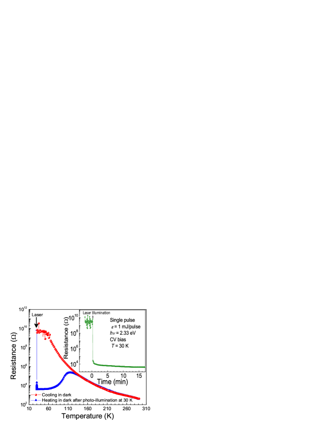
In Fig. 1 we show the temperature (T) dependence of the sample resistance (R), measured in the CV mode, during cooling (filled circles). The resistance is thermally activated with a temperature dependent activation energy down to 60 K. For T 60 K, the sample resistance exceeds the input impedance of the nanovoltmeter. At 30 K, the sample was irradiated with 30 pulses ( 6 ns) of 532 nm (photon energy h = 2.33 eV) radiation at 5 Hz each of energy () 1 mJ/pulse. The sample resistance dropped by 5 orders of magnitude upon the incidence of the first pulse. The subsequent pulses reduce the resistance only marginally from 3104 to 4103 . The electrical state of the material after photo-irradiation is metallic as can be seen from the positive dR/dT of the resistance curve on warming the sample (filled triangles). Moreover, the photoinduced metallic state persist even after switching off the electric field. In the inset of Fig. 1 we show the result of a similar experiment where the sample was cooled to 30 K from room temperature (300 K), irradiated with a single laser pulse and the resistance was monitored as a function of time under isothermal conditions. The resistance drops almost instantaneously upon the incidence of the pulse followed by a much slower diffusive type of enhancement in the conductivity.
Now we establish the complementarity of the photon flux and electric field in inducing the I-M transition. In Fig. 2(a) the current (i) - electric field (E) characteristics of the sample in dark at 80 K are shown. For the first scan with increasing bias field the current initially increases as i En, n 1.16. This small deviation from the ohmic behaviour (n = 1) is also seen in the R-E plot of Fig. 2(b). However, when the electric field across the sample exceeded a critical value EC ( 9 kV/cm), the resistance drops abruptly by a factor of 10 indicating an electric field induced switching. We denote the maximum electric field applied across the sample as Emax and the corresponding resistance Rmin. On decreasing E the resistance remains around Rmin for high electric fields and then starts increasing when E falls below 5 kV/cm. This E-field induced metallic state is persistent as is evident from the fact that a second i-E scan follows the decreasing E branch of the first scan. However before we attribute this spectacular effect to any fundamental process such as field induced melting of the charge ordered state, the role of simple Joule heating in triggering this transition needs to be looked into. The following observations suggest that the effects seen here is not a consequence of heating; (1) Power dissipated in the circuit even at the peak current is 1 mW. (2) The i-E curves in repeated cycles performed at the same temperature over a period of several hours are ohmic with several orders of magnitude lower resistance. This is not expected in the case of Joule heating in which case the sample should come back to its virgin state when the source of heat is removed. (3) Similar i-E measurements on some insulating non-charge ordered manganites LaMnO3, Sm0.55Sr0.45MnO3 do not show current switching effects. These observations clearly indicate that the electric field and perhaps the associated current, but not the heat induces a structural/electronic phase change in the material, which is healed only after heating the sample above its CO temperature.
After heating the sample to 300 K and cooling it back to 80 K we did another i-E measurement in dark, as shown in Fig. 2(c) ( filled circles), but this time the electric field was kept below EC ( 9 kV/cm). As expected, we did not see any E-field induced switching. This was followed by another i-E measurement in the presence of a magnetic field (H) of 3,400 gauss applied in the plane of the film. As seen in Fig. 2(c), a sharp jump in the current is observed at a field strength of 4 kV/cm, which is lower than the zero-field value of the switching field (EC). Yet again the high conductivity state is persistent. While the observed I-M transition is not purely a magnetic field induced effect as an assisting electric field was required, the application of the magnetic field brings down the EC substantially. Finally, the sample was once again cooled to 80 K after heating it to room temperature. Two successive i-E scans were made in dark and E EC to ensure the stability of the insulating state . After the end of the second scan, the sample was irradiated with 30 pulses of 2.33 eV radiation and the i-E scans were taken again, the result of which are shown in Fig. 2(d). As seen from the graph, there is a clear drop in the resistance after photo-irradiation although this drop is much smaller as compared to the drop at 30 K.
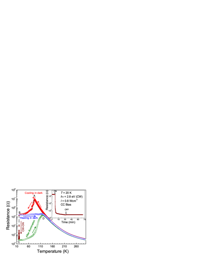
In Fig. 3 we show results of R-T measurement in the CC mode. For T 85 K, the cooling curve (filled circles) in dark is identical to the cooling curve of the CV mode (Fig. 1). Below 85 K, however, the behaviour of R-T is different from the CV data. Here the resistance starts decreasing below T 85 K and reaches a value of 0.15 M at 20 K. This decrease can be attributed to a voltage-induced melting of the CO state. Unlike the CV measurement, the electric field across the sample in a CC measurement is not constant. It increases to ensure a constant current as the sample resistance rises on lowering the temperature. At T 85 K, the field becomes comparable to EC and the resistance exhibits a downturn. However, as R goes down, the sample bias voltage also decreases in order to maintain the CC condition. While this feedback mechanism arrests a precipitous drop in resistance, a gradual lowering of R with decreasing temperature continues since the threshold electric field EC also decrease as the temperature goes down. Upon heating the sample from 20 K, the resistance remains constant around 0.15 M till 120 K and then falls following the cooling curve. In a second R-T measurement, the sample was cooled to 20 K in dark (filled triangles) followed by photo-illumination with 2.8 eV CW radiation of intensity 0.8 Wcm-2 for 25 mins. The laser radiation was then cut off and the resistance monitored as a function of time for the next 40 mins while holding the temperature at 20 K. As seen clearly, the photo-illumination decreases the resistance by 3 orders of magnitude. It is evident that in the CC measurements the switching transition occurs in two steps, each leading to the conversion of a certain fraction of the material to the metallic phase. The first state is initiated by the electric field at 85 K . Although the stimulus acts uniformly across the bridge, the breakdown presumably takes place along the weakest path, thereby creating only a few percolating channels through which majority of the current flows leaving most of the sample in the original charge ordered insulating state. The second step is photo-excitation of carriers across the charge-order gap and creation of new metallic patches which eventually coalesce and create more percolative channels. In the inset of Fig. 3 we show the time dependence of sample resistance at 20 K during exposure and after exposure to 0.8 Wcm-2 CW radiation of energy 2.8 eV. During exposure the sample resistance drops, first abruptly and then very slowly with time. Once the laser is switched off no noticeable change in the resistance is seen over an extended period of time ( 2,400 s). This observation rules out the possibility that the PIMT is caused by laser heating as 2,400 seconds is a long enough time for the sample to thermalize. The similarity of the curves obtained on heating the sample in dark from 20 K to 300 K after photo-illumination at 20 K, and heating from 20 K to 300 K with the laser beam on during the heating (not shown), further suggested that thermal effects of laser irradiation are insignificant.
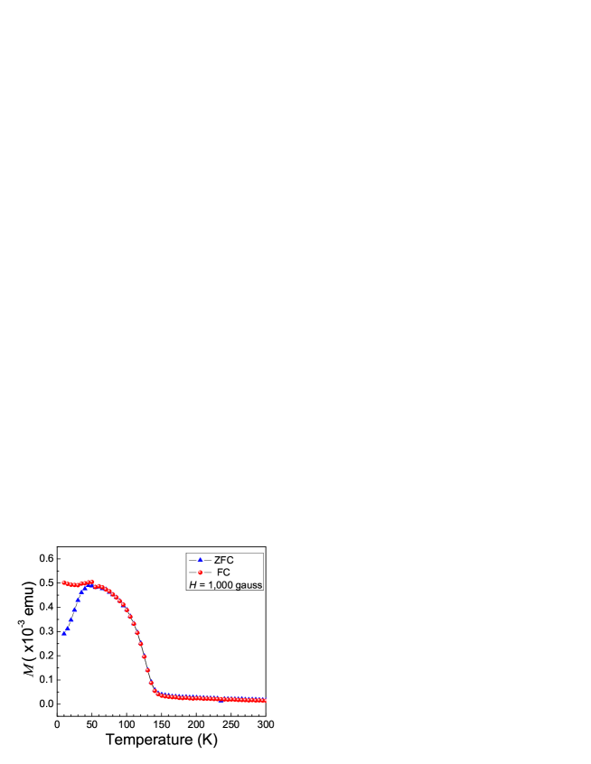
The distinct peak in resistance at 120 K on warming the sample after light exposure can be related to the magnetic transition in the system. Figure 4 shows the zero-field-cooled (ZFC) and field-cooled (FC) magnetization of the sample measured between 10 K and 300 K. Although an absolute measurement of the ordered moment per Mn site of the sample is difficult in the present case due to the large paramagnetic contribution from the substrate (NGO), the data clearly show onset of spontaneous magnetization at T 140 K. The fraction of the ferromagnetic phase which is also metallic is, however, not large enough to yield signature of this magnetic transition in the R vs T plot. But on photo-illumination, the phase become large enough to open a percolating path. The peak in the resistivity at T 120 K can be attributed to the ferromagnetic (FM) to paramagnetic (PM) transition as seen in other manganites such as La0.7Ca0.3MnO3 coey . The density of such paths depends upon the photon flux as evident from the extent of change in resistance on CW and pulsed laser irradiation.
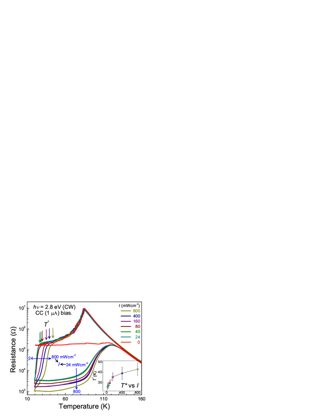
A further confirmation of this result comes from the dependence of sample resistance on intensity (I) of 2.8 eV CW radiation measured in the CC mode as shown in Fig. 5. For all the scans shown in this figure, the exposure to light was initiated at 150 K while cooling from 300 K and continued till the sample temperature reaches 20 K. During the heating cycle from 20 K to 300 K the sample remained in dark. The R vs T curves taken at different intensity of light remain the same down to 50 K as the one taken in dark. However, a precipitous drop in resistance occurs at a critical temperature T∗ ( 50 K) which scales non-linearly with the photon flux, as shown in the inset of Fig. 5. In order to understand the data we must recall that in a CC-mode measurement the changing electric field also creates a metallic phase in addition to the conducting phase fraction p resulting from photo-irradiation. Since for the higher photon flux, the induced metallic phase is already large, a small contribution to p from the electric field is required such that the total reaches , the percolation threshold. This is the reason why T∗ moves up progressively with the photon flux (inset Fig. 5). It is also interesting to note that the resistance reached at 20 K on photo-exposure is progressively smaller with the increasing photon flux.
It is interesting to note that a somewhat similar IMT initiated not by a CW laser but a broad band xenon lamp has been seen in oxygen deficient La2/3Sr1/3MnO3 and Pr2/3Sr1/3MnO3 filmsgilabert ; cauro2 . While these authors have attributed the IMT to photo induced electron-hole pair generation, where electrons are trapped at oxygen vacancies and the free hole contribute to conduction, doubts about probable heating effects have been raised cauro2 . While our experiments with pulsed laser light clearly show that the photo-induced metallic state is persistent (survives after removal of the light as long as the temperature is not raised beyond TCO), we put this issue of sample heating to rest by performing CW photoexposure experiments at the highest intensity on fully oxygenated manganite thin films of insulating ground state such as LaMnO3 and Sm0.55Sr0.45MnO3. These films are of similar geometry and thickness deposited on substrates (LaAlO3 and SrLaAlO4) of similar thermal conductivity. We do not see any perceptible drop in the resistance of the samples on photoexposure. The temperature rise due to heating is only about 1.7 K/Watt cm-2 at T 76 K. The resistance of the final state reached after photo-illumination with different intensities and different durations of exposure can be understood qualitatively by considering excitation of electrons from Mn3+ to Mn4+ and thus a local disruption of the CO state. We believe these disruptions first localize in the form of small polarons, then grow into large polarons and finally form a conducting channel with the increasing photon flux.
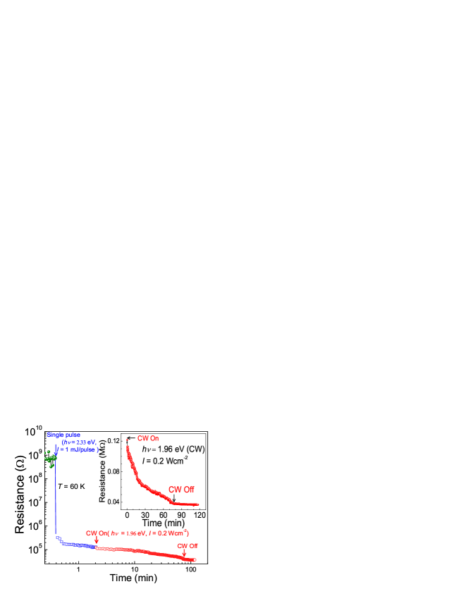
In Fig. 6 we show the effect of photo-illumination with a single shot of 2.33 eV ( = 1 mJ/pulse), followed by exposure to 1.96 eV CW (I = 0.2 Wcm-2) laser radiation for about 75 mins. This measurement was performed in the CV mode at 60 K. We note that the 2.33 eV pulse leads to a 4 orders of magnitude drop in resistance and the subsequent CW-beam causes a negligible further drop. Contrary to a previous report takubo , no annealing effects of CW laser irradiation which lead to the recovery of the original insulating state is seen at these intensities.
IV Conclusion
In conclusion, we have observed a persistent photo-induced I-M transition in La0.175Pr0.45Ca0.375MnO3 thin films. Our observations point to the fact that electric, magnetic and photon fields acting independently induces metallic domains in the sample. A complementary role of these stimuli is seen from the enhancement of the effect when two of them are applied simultaneously. Although these different perturbations couple to different internal degrees of freedom, like the magnetic field couples to the spin system where as light and electric fields couple to the charge, a strong correlation among these degrees of freedom causes a collapse to the same final state. Moreover, this particular manganite appears to be the only one discovered till date where all the degrees of freedom are susceptible to perturbations of comparatively smaller magnitude. The localized nature of the persistent photo-induced I-M transition in conjunction with the fact that the metallic and the insulating regions will have different refractive index and also different Kerr rotation weisheit , if they can be shown unambiguously to be ferromagnetic due to the state of the metallic clusters, make this material promising for magnetic and optical memory application. The need of pump-probe experiments to see Kerr rotation after photoexposure is important.
Acknowledgements.
This research has been supported by grants from the Indo-French Center for the Promotion of Advanced Research New Delhi and the Board of Research in Nuclear Sciences (BRNS) Government of India. We thank R. Sharma for technical assistance in magnetization measurements and Navneet Pandey for depositing films of LaMnO3 and Sm0.55Sr0.45MnO3 which were used to estimate the heating effect.References
- (1) Salamon M. B. and Jaime M., Rev. Mod. Phys., 73, 583 (2001).
- (2) Tokura Y. and Tomioka Y., J. Magn. Magn. Mater., 200, 1 (1999).
- (3) Coey J. M. D., Viret M. and Von Molnar S., Adv. Phys., 48, 167 (1999).
- (4) Rao C. N. R. and Raveau B. Colossal Magnetoresistance, Charge-ordering and Related Aspects of Manganese Oxides, World Scientific, Singapore, 1998.
- (5) Mathur N. and Littlewood P., Physics Today, 56, 25 (2003).
- (6) Asamitsu A., Tomioka Y., Kuwahara H. and Tokura Y., Nature, 388, 50 (1997).
- (7) Tomioka Y., Asamitsu A., Kuwahara H., Moritomo Y., Kasai M., Kumai R. and Tokura Y., Physica B, 237, 6 (1997).
- (8) Hwang H. Y., Palstra T. T. M., Cheong S- W. and Batlogg B., Phys. Rev. B, 52, 15046 (1995).
- (9) Urushibara A., Moritomo Y., Arima T., Asamitsu A., Kido G. and Tokura Y., Phys. Rev. B, 51, 14103 (1995).
- (10) Akahoshi D., Uchida M., Tomioka Y., Arima T., Matsui Y. and Tokura Y., Phys. Rev. Lett., 90, 177203 (2003).
- (11) Tokura Y., J. Phys. Soc. Jpn., 75, 011001 (2006).
- (12) Miyano K., Tanaka T., Tomioka Y. and Tokura Y., Phys. Rev. Lett., 78, 4257 (1997).
- (13) Gilabert A., Cauro R., Medici M.G., Grenet J.-C., Wang H.S., Hu F. and Li Q., J. Supercond., 13, 285 (2000).
- (14) Cauro R., Gilabert A., Contour J. P., Lyonnet R., Medici M.-G., Grenet J.-C.,Leighton C. and Schuller Ivan K., Phys. Rev. B, 63, 174423 (2001).
- (15) Takubo N., Ogimoto Y., Nakamura M., Tamaru H., Izumi M. and Miyano K., Phys. Rev. Lett., 95, 017404 (2005).
- (16) Kiryukhin V., Casa D., Hill J. P., Keimer B., Vigliante A., Tomioka Y. Tokura, Y., Nature, 386, 813 (1997).
- (17) Hervieu M., Barnabé, A. Martin, C. Maignan, A. Raveau B., Phys. Rev. B, 60, R726 (1999).
- (18) Budhani R. C., Pandey N. K., Padhan P., Srivastava S. and R. Lobo, Phys. Rev. B, 65, 14429 (2002).
- (19) Rairigh Ryan P., Singh-Bhalla Guneeta, Tongay Sefaatin, Dhakal Tara, Biswas Amlan and Hebard Arthur F., Nature Physics, 3, 551 (2007).
- (20) Weisheit M., Fähler S., Marty A., Souche Y., Poinsignon C. and Givord D., Science, 315, 349 (2007).