Detailed Studies of Pixelated CZT Detectors Grown with the Modified Horizontal Bridgman Method
Abstract
The detector material Cadmium Zinc Telluride (CZT) achieves excellent spatial resolution and good energy resolution over a broad energy range, several keV up to some MeV. Presently, there are two main methods to grow CZT crystals, the Modified High-Pressure Bridgman (MHB) and the High-Pressure Bridgman (HPB) process. The study presented in this paper is based on MHB CZT substrates from the company Orbotech Medical Solutions Ltd. [1]. Former studies have shown that high-work-function materials on the cathode side reduce the leakage current and therefore improve the energy resolution at lower energies. None of the studies have emphasized on the anode contact material. Therefore, we present in this paper the result of a detailed study in which for the first time the cathode material was kept constant and the anode material was varied. We used four different anode materials : Indium, Titanium, Chromium and Gold, metals with work-functions between 4.1 eV and 5.1 eV. The detector size was 2.02.00.5 cm3 with 88 pixels and a pitch of 2.46 mm. The best performance was achieved with the low work-function materials Indium and Titanium with energy resolutions of 2.0 keV (at 59 keV) and 1.9 keV (at 122 keV) for Titanium and 2.1 keV (at 59 keV) and 2.9 keV (at 122 keV) for Indium. Taking into account the large pixel pitch of 2.46 mm, these resolutions are very competitive in comparison to those achieved with detectors made of material produced with the more expensive conventional HPB method. We present a detailed comparison of our detector response with 3-D simulations. The latter comparisons allow us to determine the mobility-lifetime-products (-products) for electrons and holes. Finally, we evaluated the temperature dependency of the detector performance and -products. For many applications temperature dependence is important, therefore, we extended the scope of our study to temperatures as low as -30∘C. There are two important results. The breakdown voltage increases with decreasing temperature, and electron mobility-life-time-product decreases by about 30% over a range from 20∘C to -30∘C. The latter effect causes the energy resolution to deteriorate, but the concomitantly increasing breakdown voltage makes it possible to increase the applied bias voltage and restore the full performance.
keywords:
CdZnTe, CZT detectors, temperature dependencyPACS:
95.55.Ka1 Introduction
Cadmium Zinc Telluride (CZT) has emerged as the material of choice for the detection of hard X-rays and soft gamma-rays with excellent position and energy resolution and without the need for cryogenic cooling. The high density of CZT ( 5.76 g/cm3) and high average atomic number ( 50) result in high stopping power and in a large cross section for photoelectric interactions.
The main application of CZT detectors is the detection of photons in the 10 keV to 1 MeV energy range. CZT has a major impact in various fields including medical imaging, homeland security applications, and space-borne X-ray and gamma-ray astronomy.
To give a few examples of the latter, the Swift mission launched in 2004
carries a wide field of view X-ray telescope for the discovery of gamma-ray
bursts (GRBs) in the energy range from 15 keV to 150 keV [2].
This Burst Alert Telescope makes use of the coded mask technique to localize
GRBs with an accuracy of 1-2 arcmin. It is built out of an array of 32,768
co-planar 244 mm3 CZT detectors covering a total area of
0.5 m2. The proposed EXIST (Energetic X-ray Imaging Survey Telescope)
mission [3] also uses the coded mask approach.
With 15,000 pixelated CZT detectors, each with a volume of 2.02.00.5 cm3 and with 1616 pixels, an angular resolution of 5 arcmin will be achieved and the energy range between 10 keV and 600 keV will be covered.
In this paper, we present a detailed study of CZT grown with the Modified
Horizontal Bridgman (MHB) process by the company Orbotech Medical Solutions
Ltd. [1] (previously Imarad). This growth technique gives uniform
substrates at high yields and thus modest costs. One of the disadvantages of
the MHB technique is a somewhat lower bulk resistivity of cm
compared to cm obtained with the more conventional High
Pressure Bridgman (HPB) process. This results in higher leakage currents and therefore degrades the energy resolution at lower energies ( 100 keV).
Several authors recognized that it is possible to reduce dark currents in MHB detectors by using p-type-intrinsic-n-type (PIN) and metal-semiconductor-metal (MSM) contacts [4, 5, 6, 7, 8]. Both schemes, PIN and MSM, can indeed reduce the dark currents by factors 10 and improve on the energy resolution of the detectors at low ( 100 keV) energies. Encouraged by the result of these authors, we experimented with different cathode and anode materials on several MHB substrates, optimizing for the first time the cathode and anode contacts separately. We discussed a comparison of different cathode materials in an earlier paper [9]. Gold (Au) was among the metals yielding the best performance in terms of dark current suppression and energy resolution as cathode contact material. With the objective to finalize our studies on contact materials, we present in this paper the results on different anode contact materials with an Au cathode and added a study of the performance at lower temperatures which is especially important for space borne applications. We derived -products of electrons and holes needed for detector simulations. These reproduce the measured data well, and can be used to further improve detector performance and design.
The paper is structured as follows:
In section 2, origin and some general properties of our substrate
are presented. We explain how we used this substrate to fabricate detectors suited for our measurements and give a short description of our experimental setup. Then in section 3, we discuss crystal inhomogeneities and present the results of photoluminescence mapping of the Zn content and of infrared transmission microscopy. Subsequently, in section 4, the choice of the contact materials is explained, and the design of the detectors we used for comparison measurements is described in detail. Section 5 presents the results of our comparison experiments and a discussion of the
influence of anode contact materials on the performance. In section 6, we show that we can reproduce experimental data with computer simulations. For this, -products of electrons and of holes need to be known. We explain how we measured the -products of electrons and used simulations to derive the -products of holes. In section 7, we present studies of the temperature dependence on the detector response and the electronic properties of CZT.
2 Substrate, detector fabrication and setup for performance measurements
As CZT substrate, we used a detector from Orbotech Medical Solutions Ltd. [1] grown by the Modified High-Pressure Bridgman (MHB) process, delivered with a monolithic Indium (In) cathode, and 88 Indium anodes (pixels). The size of the wafer was 2.02.00.5 cm3, the pitch of the pixels (anode contacts) 2.46 mm, and the gap between the pixels 0.6 mm. In order to minimize unknown parameters, we used a newly delivered CZT detector from which we removed the original contacts and deposited new ones using the following procedure.
In a first step, the original contacts were removed by polishing with abrasive paper, followed by fine polishing with 0.5 m particle size alumina suspension, and then by rinsing clean with pure methanol. During the polishing process, the quality of the polished surface was constantly monitored with an optical microscope. Afterwards, the detector was etched for two minutes in a 1% bromine-methanol solution and subsequently rinsed with methanol. Metalization was performed with an electron beam evaporator keeping the original geometry: pixel pitch 2.46 mm, gap between pixels 0.6 mm. A temperature sensor was used to ensure that the substrate temperature never exceeded 100∘C.
For the performance measurements, we used a custom-designed PC card with 88 contact pads, which had a Delrin [10] plastic fixture to mount the detector. Gold-plated, spring-loaded pogo-pins were used to connect the anode pixels to the PC Card, which fans out the contacts to the readout electronics. The cathode was biased at -1000 V, while the anode pixels were held at ground potential. A hybrid electronic readout was used to read out the central 16 pixels of the detector. Three of the pixels in the center of the crystal and the cathode (4 channels) were read out with a fast Amptek 250 amplifier. The post-amplified signals were digitized with a 4-channel 500 MHz oscilloscope, and transferred via Ethernet to a personal computer. This set-up allows us to measure the pulse length, and thus the drift times of the charge carriers with an accuracy of 10 ns at 662 keV. The signals from the other 13 pixels were read out with an ASIC111ev Products, ev-MultiPIX and a custom designed VME board. Therefore, we used only information of the central 16 pixels. Figure 1 shows a schematic view of the anode side in which these pixels are highlighted gray. Additionally, we monitored the noise of the readout electronics with a pulser: both readout chains have a FWHM noise of 4 keV. Energy spectra were taken at 59 keV (241Am), 122 keV (57Co), and 662 keV (137Cs).
3 Substrate characterization
The Zn-fraction (x) in a Cd1-xZnxTe sample determines the bandgap and therefore the energy required for the production of electron-hole pairs. A 1% variation of the zinc fraction corresponds roughly to a 0.5% shift of the photopeak position. In the case of pixelated detectors, a variation in Zn fraction does not necessarily influence the performance, since each individual pixel’s spectra can be corrected based on simple calibration measurements. But, when we compare the performance of individual pixels on the same substrate, we have to exclude the possibility that local differences in crystal structure and composition are the cause of the observed effects. Therefore, the group at Fisk University used a photoluminescence method to map the zinc content, and infrared transmission microscopy to determine crystal defects of the CZT substrate.
3.1 Zn content photoluminescence mapping
Photoluminescence (PL) mapping techniques [11] normally use laser light having an energy above the bandgap of the crystal to illuminate the sample. Photons are absorbed and electronic excitations are created. If through radiative relaxation light is emitted, the process is called photoluminescence. For each spot on the crystal wafer, this emitted PL light is collected and fed into a spectrophotometer. The acquired PL spectra are fitted and the peak wavelength determined. From the peak position, the Zn-fraction (x) is calculated. [12, 13, 14].
Our PL mapping system operated at room temperature and used a 20 mW He-Ne laser (= 633 nm), a 10.1610.16 cm2 X-Y stage, and a S2000 Miniature Fiber Optic Spectrometer from Ocean Optics. LabVIEW-based GUI software was developed by the group at Fisk University to perform automatic scanning, PL spectra acquisition, PL peak position analysis as well as to display in false color the Zn index (x) or Zn concentration on the surface of CZT sample.
Sample preparation consisted of fine polishing without etching.
The results are shown in Fig. 2. The Zn fraction varies on the anode side between 0.110 and 0.135, on the cathode side between 0.120 and 0.135. Toney et al. [13] performed similar room temperature PL mappings of HPB samples, which were 2 mm thick and had an area of 1-2 cm2. These samples were etched in a 0.5% bromine-methanol solution for 7 minutes. They showed a Zn fraction fluctuation of 1-2% within one sample, and 5%-10% between the top and the heel of a 13 cm long boule. This variation is smaller than in our substrate. But, this may be due to the fact that our samples were not etched, since Li et al. [15] reported that etching the substrates improves surface quality and reduces the Zn-fraction variations.
3.2 Detection of crystal defects with infrared transmission microscopy
Microscopy in infrared (IR) light of a wavelength, where CZT is sufficiently transparent, was used to localize crystal defects. In the case of CZT these are mostly Tellurium (Te) inclusions and grain boundaries. We used unpolarized IR light with a wavelength of 960 nm to reveal the general condition of the crystal. Polarized light with a wavelength of 1150 nm was used to determine the stressed regions in the CZT substrate. With a polarizer oriented at right angles with respect to the plane of polarization, unstressed material produces a dark field of vision. Because stress generates birefringence, stressed regions are seen bright on a dark background. In Fig. 3 only Fig. 3.2 was taken with polarized light.
In Figure 3, left hand side, the image of the whole substrate is shown. There are some defects visible mainly in the outer region of the detector which we did not use for evaluation of detector performance. These defects are surface scratches caused by the detector holder and the gold plated pogo-pins (Fig. 3: 1, 2). In the central region relevant for our measurements, only one major defect is visible. This defect is shown with higher resolution in Fig. 3: panels 3.1. (unpolarized) and 3.2 (polarized). The defect is most likely a crack with Te inclusions. Using Fig. 3: 3.2 one finds that it covers a region of about 1 mm2. It is localized about 200 micron below the anode side. We will show later that the pixel in which the defect is located has an inferior performance compared to the others. We excluded this pixel from the analysis.
4 Choice of contact materials and detector design for comparison tests
As already mentioned in section 1, one of the disadvantages of the MHB method is the lower bulk resistivity, compared to crystals grown with the HPB method, causing high leakage currents that contribute to the intrinsic noise and deteriorate the performance of detectors at low energies ( 100 keV). The possibility to reduce bias currents by using high work-function (WF) blocking contacts on the cathode side of the n-type CZT was discussed by various authors (e.g. [4, 9, 5]).
Nemirovski et al. [4] reported on the characterization of three types of contact configuration: first, ohmic In contacts on both, anode and cathode side, second, rectifying Au contacts on the cathode side with In contacts on the anode side, third, non-ohmic contacts on both, anode and cathode side (Au and Aluminum (Al)). At 122 keV, he obtained an energy resolution of 5.2%, 4.6%, and 7% for the three configurations respectively. Vadawale et al. [5] presented results of 20 CZT substrates. The contacts were either standard In, Platinum (Pt), Au or hybrid contacts, i.e. Pt on the cathode side, and In, or Al on the anode side. Their best energy resolution was 5.0% at 122 keV with Pt contacts followed by 5.7% with Au contacts. They found also that the detector uniformity depends on the anode contact material: low work-function material on the anode side produces a more homogeneous response throughout the detector.
While these studies give interesting hints, it is still unknown which is the best choice of anode contacts. Therefore, we decided to study anode contact materials with a broad range of work-functions. We chose In, Ti, Cr, and Au with work-functions of 4.12 eV, 4.33 eV, 4.50 eV and 5.10 eV respectively for our comparison experiment. We excluded Pt (work-function: 6.35 eV) because substrates with Pt contacts showed poor performance when the deposition was done with the help of an electron beam system (for more details see [9]). As cathode contact material, we used Au, since our earlier study (see [9]) has shown that Au reduces the dark current and improves the energy resolution.
The surface and detector treatment before and during contact deposition influences the detector performance. Therefore we deposited the four different metals on a single detector substrate using a quarter of the 64 pixels for each material as shown in Fig. 4. This design (4M-detector) ensures that all pixels have the same history. There remains another important point. One has to make sure that performance differences between different contact materials are not caused by substrate inhomogeneities. In section 3, we described already some of our precautions. Additionally we fabricated a detector from the same substrate chip, where instead of four different materials only one, Ti, was used (Ti-detector). In this way we were able to compare pixels of the four sectors under identical conditions.
5 Results of performance measurements comparing anode materials
The results discussed in this section relate to only 15 of the 16 central pixels. One pixel was removed from the analysis, because infrared microscopy (see Section 3) has shown a major crystal defect in the area of this pixel leading to very poor performance in both contact configurations. Energy resolutions discussed in this section are resolutions of single pixels. Signals in neighboring pixels were ignored. For higher energies (122 keV and 662 keV) the anode signal was corrected for the depth of the photon interaction (DOI) based on the cathode-to-anode signal ratio.
Table 1 summarizes the results obtained with both contact configurations for an 241Am source. The energy resolution is averaged over the three or four pixels of the 4M-detector with identical contact material and compared to an average over the corresponding pixels of the Ti-detector. The numbers are corrected for electronic noise. In parentheses, we added the uncorrected data. Both sets of data present the same picture. Therefore, we discuss the uncorrected data. Ti with resolutions of (4.20.2) keV (4M-detector) as well as (4.40.2) keV, (4.50.1) keV, (4.30.2) keV and (4.30.1) keV (Ti-detector) had obviously the best performance followed closely by In (4.80.2) keV. Au and Cr as anode contact materials are inferior by 8%: (5.30.2) keV (Au), (5.40.3) keV (Cr).
Table 2 summarizes our results at 122 keV, and 662 keV. The important result is that all four different anode materials show rather similar energy dependence on the resolution, and that the order of performance remains unchanged.
In Fig. 5, the energy spectra of a single Ti pixel are shown for three different photon energies. In case of the higher energies 122 keV (57Co) and 662 keV (137Cs), the anode signal was corrected for the depth of the photon interaction (DOI) based on the cathode-to-anode signal ratio. Given the large pixel pitch of 2.46 mm, we obtained the excellent energy resolution of 1.4 keV (4.0 keV), 2.0 keV (4.1 keV), and 7.2 keV (9.9 keV) for photon energies of 59 keV, 122 keV, and 662 keV, respectively. Again, the values given are corrected for electronic noise with the uncorrected data added in parentheses. The peak-to-valley ratio defined as the ratio of the maximal counts in the photopeak to the mean of the channels between 560 keV and 580 keV, was 15.5 for 662 keV.
Performance measurements for CZT crystals grown with the HPB process have been reported in the literature [16]. The energy resolution was 0.73% and 0.93% at 662 keV for two different detectors. Besides a different production process, there are other important features in which our setup varies from theirs. The substrate measured 1.51.51.0 cm3 with 1111 anode pixels and a pitch 1.27 mm. A steering grid between pixel anodes was used which was biased at negative voltage to focus the electrons to the anodes. The grid electrode was 100 m wide and had a 200 m gap between grid and pixel. These differences, one has to keep in mind when comparing both experiments, because these parameters have a strong influence on the energy resolution. A smaller pixel pitch and a larger thickness enhances the small pixel effect. Using simulations we have shown, that an increase in the thickness from 0.5 cm to 1 cm for a CZT detector with pixel pitch 1.64 mm will improve the energy resolution by 30% (for more details see [17]). Additionally we have compared simulated detectors with our geometry and the one used by Zhang et al. [16] but without a steering grid and found that the energy resolution is 40% better in the latter case. Taking this into account and the fact that a steering grid will further improve the resolution, we conclude that the resolution, we obtained, is comparable to the energy resolutions reported by Zhang et al.[16] of 5.0 keV and 6.2 keV at 662 keV.
6 Detector simulations
In this section, we first describe 3-D simulations of the detector response. Subsequently, we present measurements and detailed comparisons of the simulated and experimentally measured detector response which allow us to determine the -products for electrons and holes.
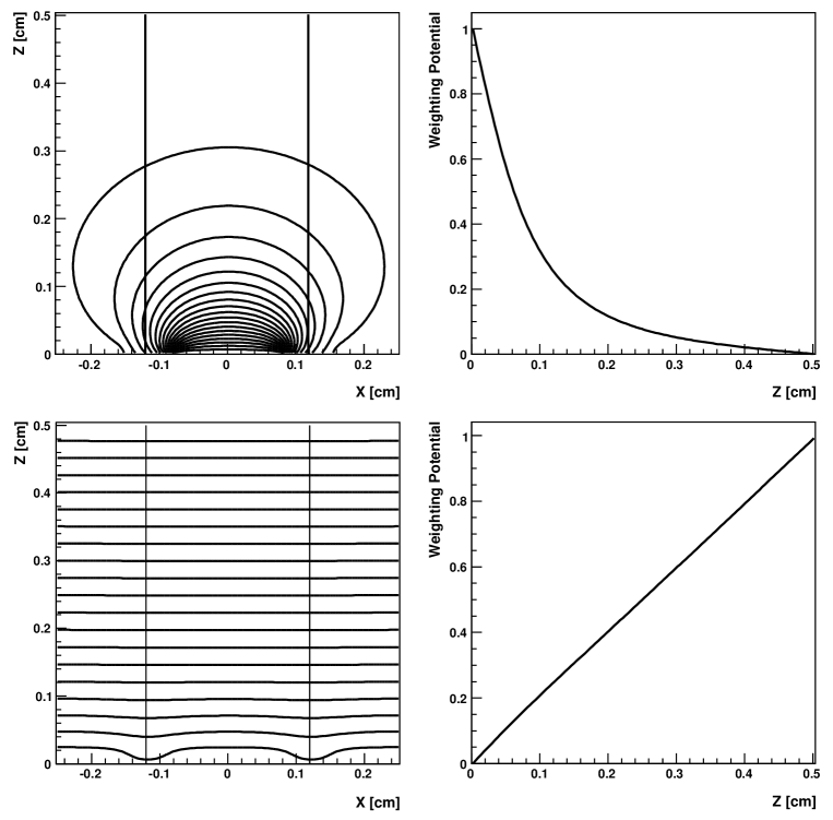
We simulated a 2.02.00.5 cm3 detector with 88 pixels with a pixel pitch of 2.46 mm and a monolithic cathode. The simulation package consists of three components (for further details see [17]). The first component calculates with a finite-difference method the 3-D electric field as well as the weighting potentials of the pixel and cathode contacts. In the second, the Geant 4.0 code [18] is used to simulate the interactions of the incident rays and the secondaries produced in the detector. The third component uses the information, where the primary photons deposit energy in the detector to generate electrons and holes, and tracks them through the detector. This component uses the electric field and the weighting potentials to compute the charge induced on the contacts. Electrons reaching the substrate surface in the gap between the pixels were left at the position, where they hit the surface, i.e. the surface conductivity was set to infinity. The detector material was assumed to be uniform. We measured electron mobility as well as electron lifetime and used these values as input parameters in our simulations. Hole mobilities and lifetimes were determined from comparisons of simulated and experimental data.
The weighting potentials of a central pixel and the cathode contact are presented in Figure 6. The graphs show a small-pixel-effect [19, 20], i.e. the pixel weighting potential has a steep gradient close to the pixel. As the pixel pitch (2.46 mm) is roughly comparable to the detector thickness (5 mm), the small-pixel-effect is not very pronounced. Therefore, electrons and holes induce charge on the anode, even if they move deep inside the detector. The cathode signal does not show any small-pixel-effect and depends almost linearly on the distance from the cathode contact.
The first step in the determination of electron mobility and lifetime is the measurement of the electron -product (), which can be calculated applying formula 1:
| (1) |
where is the detector thickness, and and are the photopeak centroids for two different bias voltages and [21]. A low energy source has to be used to ensure that most of the interaction occurs near the cathode, and that hole contributions can be neglected.
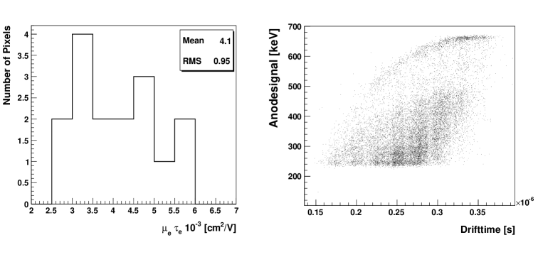
The left panel of Fig. 7
shows the -product for the central 16 pixels.
The mean is cm2 V-1 and the RMS is 0.95.
The -product of HPB CZT substrates are given
by F. Zhang et al. [16] and by S. Barthelmy et al. [2].
F. Zhang et al. [16] reported the -product of two different HPB CZT substrates with means of cm2 V-1 and of cm2 and RMS values of cm2 and cm2 respectively, which shows that CZT detectors grown with the MHB process have a similar mean, but a wider spread.
The -products of all 32,768 planar CZT HPB detectors (442 mm3) used in the Burst Alert Telescope(BAT) on-board the Swift Gamma-ray Burst Explorer (see section 1) were measured [2], and they vary
between 5.010-4 and 1.010-2 cm2 V-1. The variation within a single detector was not determined. These measurements show that the two detectors used by Zhang et al. have a -product above the average value of HPB CZT detectors.
The electron mobilities can be inferred from the widths (durations) of the induced anode pulses, which are mainly determined by the drift times of the electrons. The right side of Fig. 7 shows the correlation of the pulse widths and the induced anode charge. With a detector bias of -1000 V, the longest observed drift times were 0.35 sec. Thus, given that electrons drift up to 0.5 cm through the detector, we determined an electron mobility of cm2 V-1 s-1 and a mean electron lifetime of s using the previously measured mean -product.
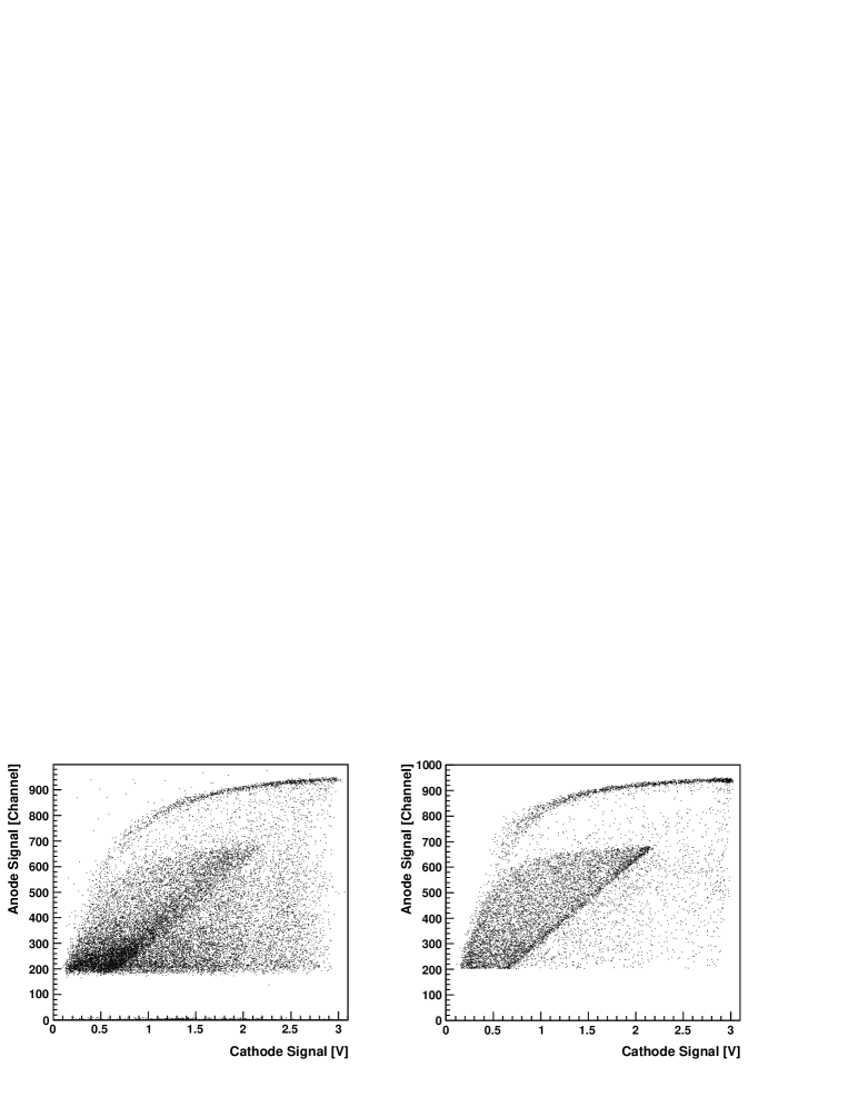
With these electron and -values, we deducted the corresponding values for holes by comparing the measured anode to cathode correlation with simulated correlations for different and . Fig. 8 right side displays the simulated correlation with cm2 V-1 s-1 and s and for comparison the corresponding correlation of our experimental data (left side). Even the finer details of the experimental data plot are reproduced well. We used this set of parameters in all simulations. The following paragraphs will show that simulations based on these parameters reproduce the experimental data.
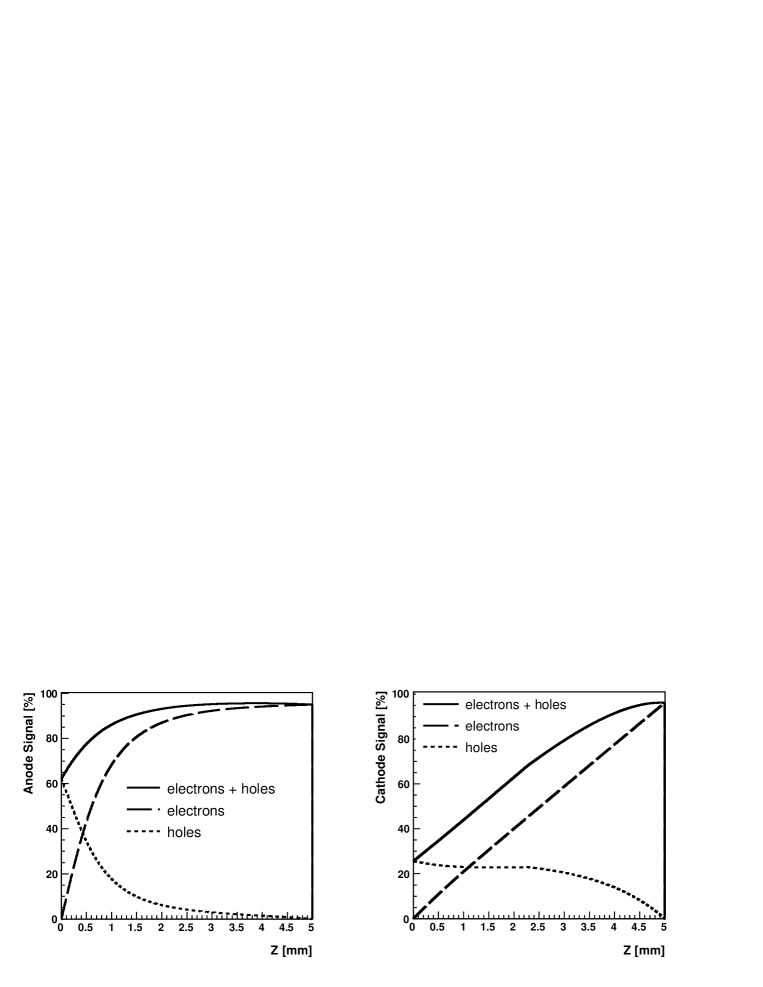
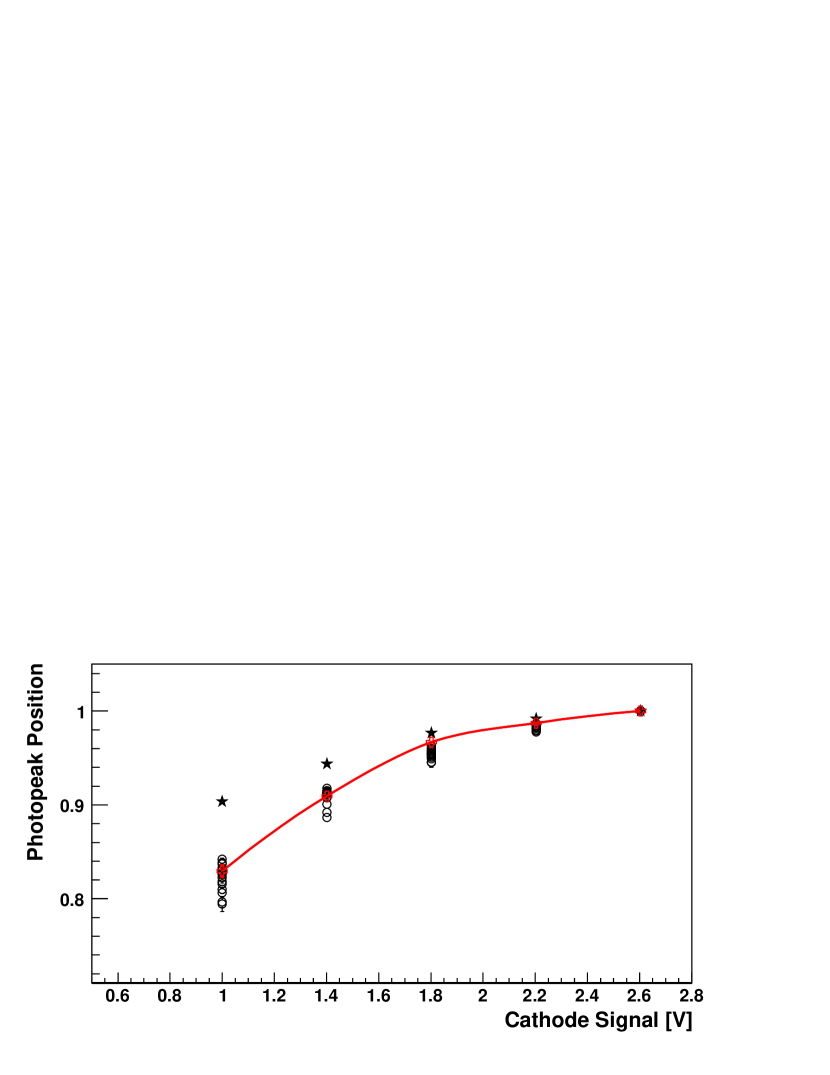
Having determined the hole parameters, we can study separately the contributions of electrons and holes to the anode and cathode signals (see Fig. 9). The anode signal dependency on the distance of energy deposition from the anode is given in the left panel of Fig. 9. The signal drops close to the anode due to the steep weighting potential increase. In this area the hole contribution is maximal and decreases to almost zero close to the cathode. The cathode signal dependency is given on the right panel. It is almost linear with the distance from the anode side. The deviation close to the cathode is caused by holes reaching the cathode before being trapped. The approximately linear dependence of the induced cathode charge on the depth of the photon interaction (DOI) can be used as a diagnostic tool to test, whether the substrate is uniform.
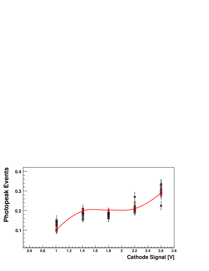
We compared the behavior of the signal dependency on the DOI by dividing the total cathode signal into five different signal ranges (0.8-1.2 V, 1.2-1.6 V, 1.6-2.0 V, 2.0-2.4 V and 2.4-2.8 V). For each interval, the position of the photopeak and the number of events in the photopeak was determined separately. The number of photopeak events is defined as the number of events lying between around the photopeak position.
The correlation of the anode versus the cathode signals depends on where in the crystal the charge is generated and to where it drifts. Figure 10 shows the measured and simulated mean photopeak positions for different intervals of the cathode signal. While the measured data consists of four different sets for each of the four materials, there is only one set of simulated data, because the contact material was not taken into account in our simulations. The agreement between data and simulations is excellent for all but one pixel. This pixel is the one which was excluded from the analysis, because infrared transmission microscopy showed the presence of a crystal defect close to the anode (section 3.2).
Figure 11 compares the measured and the simulated relative numbers of photopeak events for different ranges of the cathode signal. The measured photopeak events distribute as in the simulations, one pixel deviating more than the others. For this pixel, infrared transmission microscopy shows the presence of a crystal defect close to the anode (see Sect. 3.2).
Because the simulation matches the experimental data well, we conclude that in both cases for a given cathode signal interval the charge generation occurs in the same range of DOIs for simulation and experiment. For the deviating pixel (the same as above), the mean photopeak position varies less than for the others, confirming that the crystal defect affects the charge induced at the cathode and/or the anode. We conclude that the full volume under all but one pixel is active detector volume and produces proper cathode signals.
7 Temperature dependence
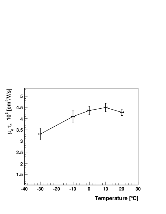
In satellite experiments ambient air temperature is well below C. Therefore we studied the dependence of the electronic properties and the performance of the CZT detector over a broad temperature range from room temperature down to -30∘C. One important parameter is the -product. It influences the detector performance. Decreasing product means inferior resolution. Therefore we measured the electron -product and the spectra as function of temperature with an 241Am source as described in section 6. Figure 12 gives the results. The product shows the highest values at and above 0∘C and decreases at lower temperatures by up to 30%. Similar behavior has been reported for HPB substrates [22] which had a maximum at 5∘C with 910-3cm2 V-1 with a drop of about 30% at -20∘ to 610-3cm2 V-1.
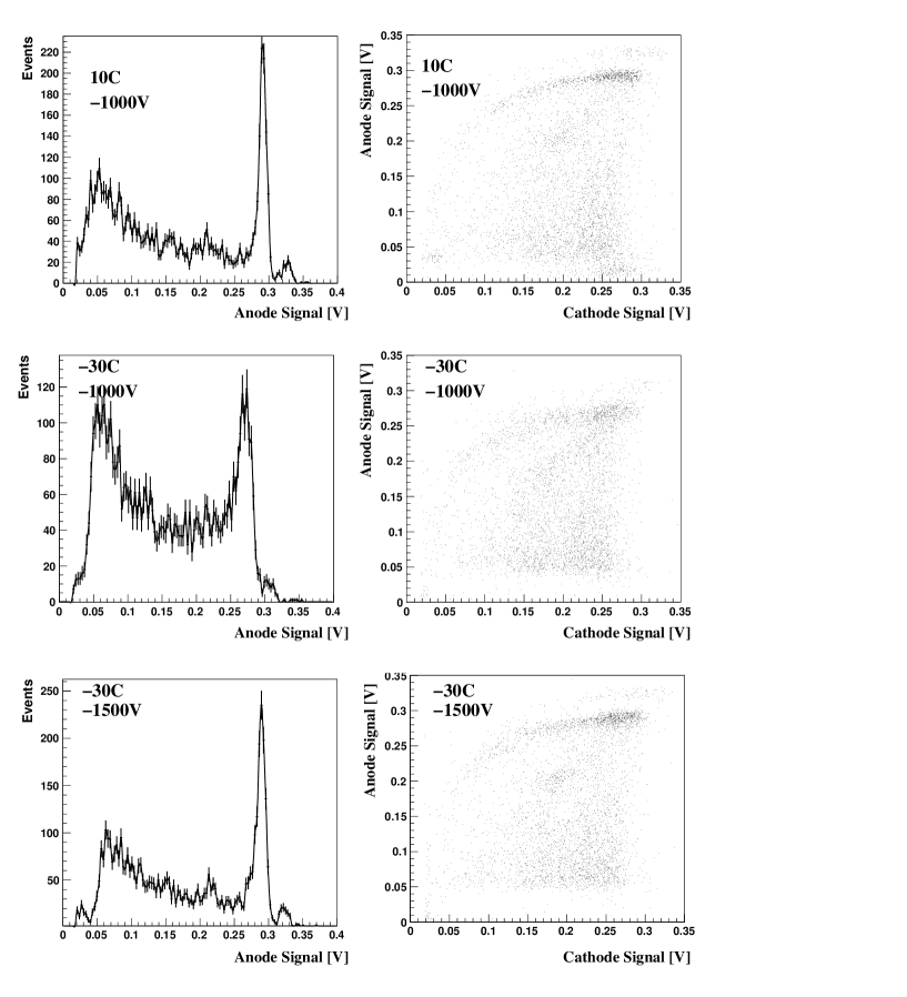
In Fig. 13 122 keV energy spectra are presented. They are measured at 10∘C and at -30∘C together with their anode to cathode signal correlations. The top two panels show that the energy resolution deteriorates markedly, when the detector is operated at lower temperatures and all other conditions (bias voltage) are kept constant. The anode-cathode correlation shows that the width of the photopeak increases for all cathode signal amplitudes, and thus for all DOIs. In the measurements that just have been discussed, we kept the bias voltage constant at -1000 V. This voltage has been chosen, because we found that at temperatures above 10∘C a change of voltage from -1000 V to -1500 V will increase the dark current by several orders of magnitude, so much, that no useful spectra could be obtained. If the detector is cooled, however, this electrical breakdown phenomenon is suppressed, and higher bias voltages become possible. The bottom panel of Fig. 13 shows an energy spectrum measured at -30∘C and a cathode bias of -1500 V. With the increased bias voltage most of the room temperature performance is recovered: energy resolution of 5.5% at -30∘C compared to 4.4% at 10∘C, and a somewhat lower signal amplitude (0.28 V and to 0.29 V respectively).
While most of the performance degradation at lower temperatures will be due to the reduction of the -product, another effect may have influenced our measurements to some extent: vibrations of the temperature chamber which was used to cool the CZT detector.
8 Conclusion
In this paper, we present the results of a detailed study of the performance
of a MHB CZT detector from the company Orbotech Medical Solutions Ltd. [1].
Using photoluminescence, we mapped the spatial distribution of the zinc content,
which showed a variation of 3%. This variation does not affect the
energy resolution of the detector if information about the location of
the interaction is available (e.g. pixelated detectors), because
in this case the effect can be corrected for.
With infrared transmission microscopy, we could detect some crystal defects and
could correlate poor pixel performance with such defects.
We tested various anode contact materials and found that Ti showed the best performance
of 2.0 keV, 1.9 keV and 7.3 keV at 59 keV, 122 keV and 662 keV, respectively.
We are using this metal now
to contact all our MHB detectors.
We showed detailed comparisons of experimentally measured and simulated
detector response. After adjusting the hole mobility and lifetime, our simulation gives
a good description of the measured data and shows that we have a deep understanding
of our data. Therefore, the simulation can be used to optimize the
detector design as the pixel width and pitch.
We studied the detector properties as a function of temperature. The electron
-product drops by about 30%, when cooling the substrate from
20∘C to -30∘C with constant bias voltage, and the energy resolution deteriorates
accordingly, a behavior that has been noted already for MHB substrates [7].
For HPB substrates, a corresponding decrease of the electron -product
has been observed [22].
We were able to recover almost all of the room temperature performance by increasing
the bias voltage at low temperatures, which is possible, because at lower temperatures the breakdown voltage is increased.
Taking everything into account, we conclude, that the overall performance of CZT detectors, produced with the cost-effective MHB process, is comparable to the performance of CZT detectors which are produced with the expensive HPB process.
Acknowledgments:
We thank Uri El Hanany from Orbotech Inc. for several free CZT detectors.
We acknowledge S. Komarov, L. Sobotka, D. Leopold, and J. Buckley for helpful discussions.
Thanks to electrical engineer P. Dowkontt, and electrical technician
G. Simburger for their support.
This work is supported by NASA under contracts NNG04WC176 and
NNG04GD70G, and the NSF/HRD grant no. 0420516 (CREST).
The authors at Fisk University gratefully acknowledge financial support
from the National Science Foundation through the Fisk University Center
for Physics and Chemistry of Materials (CPCoM), Cooperative Agreement
CA: HRD-0420516 (CREST program), and from US DOE through the National
Nuclear Security Administration (NNSA), Office of Nonproliferation
Research and Engineering (NA-22), grant no. DE-FG52-05NA27035.
References
- [1] Orbotech Medical Solutions Ltd., 10 Plaut St., Park Rabin, P.O.Box: 2489, Rehovot, Israel, 76124
- [2] S. D. Barthelmy, Proc. SPIE, 5165 (2004) 175
- [3] J. E. Grindlay & the EXIST Team 2005, New Astron. Rev., 49 (2005) 435
- [4] Y. Nemirovski, G. Asa, A. Peyser, NIM, A 458 (2001) 325-333
- [5] S. V. Vadawale et al., Proc. SPIE, 5540 (2004) 22-32
- [6] T. Narita, P. Bloser, J. Grindlay et al., Proc. SPIE, 3446 (1998) 218
- [7] T. Narita, P. Bloser, J. Grindlay, J.A. Jenkins, Proc. SPIE, 4141 (2000) 89
- [8] T. Narita, J.E. Grindlay, J.A. Jenkins et al., Proc. SPIE, 4497 (2002) 79
- [9] I. Jung, M. Groza, J. Perkins, H. Krawczynski, A. Burger, Proc. SPIE, 5922, (2005)
- [10] http://heritage.dupont.com/floater/fl_delrin/floater.shtml
- [11] T. H. Gfroerer, in: R.A. Meyers (Ed.), Encyclopedia of Analytical Chemistry, John Wiley, Chichester, (2000), pp. 9209-9231
- [12] T. E. Schlesinger et al., Mat. Sci. Eng., R 32 (2001) 103-189
- [13] J. E. Toney et al., NIM, A 380 (1996) 132
- [14] K. Hjelt et al., Phys. Stat. Sol., (a) 162 (1997) 747
- [15] Z.-F. Li et al., J. Appl. Phys., 90 (2001) 260-264
- [16] F. Zhang et al., IEEE Trans. Nucl. Sci., 52 (2005) 2009-2016
- [17] I. Jung, H. Krawczynski, S. Komarov,L. Sobotka, Astrop. Phys., 26 (2006) 119
- [18] S. Agostinelli et al., NIM, A 506 (2003) 250-303
- [19] H. H.Barret, J. D. Eskin, H. B. Barber, Phys. Rev. Lett., 75 (1995) 156
- [20] P. N. Luke, in: Proc. of the “9th International Workshop on Room-Temperature Semiconductor X- and Gamma-Ray Detectors, Associated Electronics and Applications”, Grenoble, (1995)
- [21] Z. He, G. F. Knoll, D. K. Wehe, J. Appl. Phys., 84 (1998) 5566
- [22] B. W. Sturm, Z. He, T. H. Zurbuchen, P. L. Koehn, IEEE Trans. Nucl. Sci., 52 (2005) 2068-2075

| Energy Resolution (keV) | |||
|---|---|---|---|
| 59.5 keV | |||
| Ti-detector | 4M-detector | ||
| Ti | 2.10.2 (4.40.2) | Au | 3.50.3 (5.30.2) |
| Ti | 2.10.2 (4.50.1) | Cr | 3.10.1 (5.40.3) |
| Ti | 2.0.0.2 (4.30.2) | In | 2.10.2 (4.80.2) |
| Ti | 2.00.1 (4.30.1) | Ti | 1.90.2 (4.20.2) |
| Energy Resolution (keV) | ||
|---|---|---|
| 122.1 keV | 662 keV | |
| Au | 3.30.3 (7.10.2) | 9.20.1 (11.80.2) |
| Cr | 4.30.1 (6.50.4) | 8.60.6 (11.60.4) |
| In | 2.90.1 (5.40.1) | 9.40.2 (12.60.3) |
| Ti | 1.90.1 (4.70.3) | 7.40.3 (10.40.3) |