Enhanced visibility of graphene: effect of one-dimensional photonic crystal
Abstract
We investigate theoretically the light reflectance of a graphene layer prepared on the top of one-dimensional Si/SiO2 photonic crystal (1DPC). It is shown that the visibility of the graphene layers is enhanced greatly when 1DPC is added, and the visibility can be tuned by changing the incident angle and light wavelengths. This phenomenon is caused by the absorption of the graphene layer and the enhanced reflectance of the 1DPC.
pacs:
78.40.Ri, 42.70.Qs, 42.79.FmGraphene consists of a two-dimensional honeycomb lattice of carbon atoms and has been attracting attention recently due to its remarkable electronic properties and its potential application in nanoelectronics Novoselov . Graphene exhibits high crystal quality, an exotic Dirac-type spectrum, and ballistic transport on a submicro scale. Graphene samples are usually fabricated by a micromechnical cleavage of graphite. It is difficult to distinguish the single graphene layer from many graphitic pieces, even utilizing the atomic force, scanning-tunneling, and electron microscopes. A recent experiment demonstrated that the graphene visibility depends on both the thickness of the SiO2 layer and the light wavelengthGeim . They found that specific thicknesses (300nm and 100nm) are most suitable for its visual detection for the normal light incidence and attribute this phenomenon to the opacity of the graphene layer. Although the relative difference of the reflectance [the contrast in Ref. (2)] is enhanced significantly, the absolute difference of the light reflectance is still quite low because it is determined by the weak absorption of the graphene layer. In order to enhance the visibility of graphene, i.e., the absolute and relative difference of the light reflectance of the graphene layer, we propose to prepare the graphene layer on the top of Si/SiO 2 one-dimensional photonic crystal(1DPC). This 1DPC shows a high dielectric contrast at the Si/SiO2 interface () producing a high reflectance at normal incidence, and can be fabricated by different techniques, e.g., the separation-byimplanted-oxygen techniqueNamavar , sputteringSputting combined with solid-source Si molecular beam epitaxyIshikawa , and plasma-enhanced chemical vapor depositionLipson .
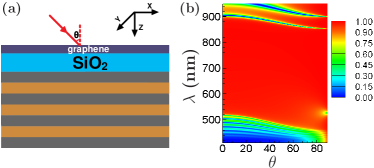
In this Letter, we investigate theoretically the light reflectance of a graphene layer prepared on the top of Si/SiO2 1DPC, as shown schematically in Fig. 1(a). We consider an asymmetric 1DPC: A0(AB)l, where is an integer denoting the l-th layer. All layers are nonmagnetic () and are characterized by their permittivities (SiO2 layer), (Si layer), and their thicknesses satisfy where is the wavelength required by the observation. The thickness of the top SiO2 layer is . We find that the difference between the reflectance of the graphene layers with 1DPC can be enhanced greatly, even one order of magnitude larger than that without 1DPC. Furthermore, the visibility of the graphene can be tuned by the incident angle.
We consider a light shedding on the graphene layer prepared on the top of Si/SiO2 1DPC with a incident angle from air (refractive index, n0 = 1). Based on the Maxwell equations for a monochrome light propagating in the medium, we have
| (1) |
where is the permittivity of the material (vacuum), the magnetic permeability of material (vacuum), and the angular frequency of the incident light.
For the TE polarization, the electric field is in the x direction, and the magnetic field is in the y-z plane, , where are the unit vectors in the x, y, and z directions, respectively. The reflected and transmitted electric fields from the 1DPC are, respectively.
| (2) | ||||
| (3) |
The electric fields of the monochrome light beam in the l-th layer is given by
| (4) | ||||
| (5) | ||||
| (6) |
where in the medium. The wavevector in a vacuum ( is the speed of light in a vacuum), but is generally complex in a medium. The electric fields of the light in the l-th layer are related to the incident fields by the transfer matrix utilizing the boundary condition , ,
| (7) |
The reflectance is defined as , and is the total layer number of the 1DPC ( in our calculation). The absolute and relative contrasts describing the difference between the reflectance with and without the graphene layer are defined as
| (8) | ||||
| (9) |
where denotes the reflectance of the sample with n-layer graphene. The latter () is the same as the definition of the contrast in Ref. [2]. In order to observe the graphene layer experimentally, both the relative contrast and the difference in reflectance between the structures with and without the graphene layer, i.e., the absolute contrast , should be large.
The parameters used in our calculation are: the refraction index , and the permittivity for graphene layer Geim ; Palik , the real and imaginary parts of the permittivity and for Si and SiO2 depending on the wavelengthSipara , the thicknesses of the SiO2 and Si layers are ( for at ) and ( for )Sipara , respectively.
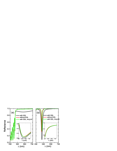
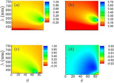
Fig. 1(b) depicts the photonic band gap of 1DPC without the graphene layer for different incident angles . The photonic band gap of SiO2(SiO2/Si)10 1DPC increases as the incident angle increases. The decrease of the reflectance in the band gap at very large incident angle is caused by the absorption in the Si layers. Fig. 2 shows the contour plots of the relative and absolute contrast and of single graphene layer (SGL) with and without 1DPC as a function of the light wavelength and the incident angle . In this figure we find that that the difference between the reflectances with and without the 1DPC exhibits a maximum at specific light wavelengths and large incident angles . This light wavelength is in the band gap of the 1DPC, i.e., the high reflection region [see Fig. 1(b)]. The maxima of the contrasts and come both from the absorption or opacity of the graphene layer and the maximum reflection of the eigenmode of the 1DPC, i.e., at normal incidence. This figure demonstrates that the reflection of the light is enhanced greatly compared to that without the 1DPC, consequently leading to a large difference in the absolute contrast between the two samples, i.e., with the 1DPC is one order magnitude (actually 20 times) larger than that without the 1DPC [see Fig. 2 (c) and (d)]. This enhancement should be helpful for the observation of the graphene. In addition, the contrasts also increase significantly with increasing the incident angle at a specific wavelength, and the maxima of the contrast shift to the shorter wavelengths such as at larger incident angles. This is due to the enhancement of the absorption of the graphene layer and the increase of the optical path length at larger incident angles . The light wavelength corresponding to the maxima of the contrasts can be tuned by changing the layer thicknesses of the 1DPC and the incident angle . This also provides us a new way to observe the graphene in the light frequency region.
In order to understand the big difference of the absolute contrast between the samples with and without the 1DPC (see Fig. 2(b) and 2(d)), we calculated the reflectance of the different structures, i.e., the layer prepared on Si substrate with and without SGL, and the layer prepared on the 1DPC with and without SGL. In Fig. 3 (a) we find that the reflectances of the 1DPC with and without SGL are both enhanced greatly compared to that without the 1DPC (see the inset of Fig. 3(a)) since the light wavelength locates at the band gap of the 1DPC. If the absorption of the SGL is neglected, i.e., (see the green lines in Fig. 3(a)), the reflectance of the 1DPC with SGL is almost same as that of the 1DPC without the SGL, i.e., the very small absolute contrast . Fig. 3(a) demonstrates clearly that the absorption of SGL and the enhanced reflection of light by the 1DPC are both important for the large absolute contrast (see Fig. 2(b)). The light reflectance of the system is determined not only by the 1DPC, but also the absorption of the graphene layer. At the large incident angle case (see Fig. 3(b)), the absolute contrast can be enhanced significantly compared with that at the normal incidence nearby the valley () of the refelctance of the 1DPC which is caused by the absorption of the Si and layers in the 1DPC, but becomes negligible small at other light wavelengths.
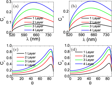
Considering the multi-layer graphene prepared on the top of the 1DPC, we plot the absolute and relative contrasts as a function of the wavelength and the incident angle (see Fig. 4). The multi-layer graphene is modeled by the corresponding number of planes separated by (the thickness of the single graphene layer). From this figure one can see that the contrasts and exhibit significant differences among the graphene layers with different thicknesses and the maximum as a function of the light wavelength and the incident angle. The difference increases as the number of the graphene layers increases. This feature makes it possible to distinguish the number of the graphene layers.
In summary, we demonstrate theoretically that the visibility of the graphene layers prepared on the top of SiO2(SiO)10 1DPC can be enhanced greatly, especially at the large incident angles and specific wavelengths in the photonic band gap. The large differences in the reflectance make it possible for the graphene layers of different thicknesses to be more easily observed and distinguished experimentally.
Acknowledgements.
This work was supported by the NSFC Grant Nos. 60525405, 90301007 and 10334030.References
- (1) K. S. Novoselov, A. K. Geim, S. V. Morozov, D. Jiang, Y. Zhang, S. V. Dubonos, I. V. Grigorieva and A. A. Firsov, Science 306, 666 (2004); Y. Zhang, J. W. Tan, H. L. Stormer and P. Kim, Nature 438, 201 (2005); A. K. Geim, and K. S. Novoselov, Nature Materials 6, 183 (2007).
- (2) P. Blake, K. S. Novoselov, A. H. Castro Neto, D. Jiang, R. Yang, T. J. Booth, A. K. Geim, E. W. Hill, arXiv:0705.0259v1 [cond-mat.mes-hall] 2 May 2007.
- (3) F. Namavar, E. Cortesi, R. A. Soref, and P. Sioshansi, Mater. Res. Soc. Symp. Proc. 147, 235 (1989); R. A. Soref, E. Cortesi, F. Namavar, and L. Friedman, IEEE Photonics Technol. Lett. 3, 22 (1991).
- (4) E. F. Schubert, N. E. J. Hunt, A. M. Vredenberg, T. D. Harris, J. M. Poate, D. C. Jacobson, Y. H. Wong, and G. J. Zydzik, Appl. Phys. Lett. 63, 2603 (1993).
- (5) Y. Ishikawa, N. Shibata, and S. Fukatsu, Appl. Phys. Lett. 69, 3881(1996).
- (6) M. Lipson and L. C. Kimerling, Appl. Phys. Lett. 77, 1150 (2000).
- (7) E. D. Palik (ed.), Handbook of Optical Constants of Solids (Academic Press, New York, 1991); H. Anders, Thin Films in Optics (Focal Press, London, 1967).
- (8) C. M. Herzinger, B. Johs, W. A. McGahan, and J. A. Woollam, J. Appl. Phys. 83, 3323 (1998).