A Silicon-Tungsten ECal with Integrated Electronics
Abstract
We summarize recent R&D progress for a silicon-tungsten electromagnetic calorimeter (ECal) with integrated electronics, designed to meet the ILC physics requirements.
To appear in Proceedings of the Linear Collider Workshop 2007, DESY, Hamburg, Germany, June 2007.
1 Overview
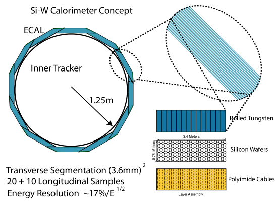
A basic physics requirement for ILC detectors is that they provide excellent reconstruction of hadronic final states. This allows access to new physics which is complementary to the LHC. One statement for a requirement on jet reconstruction is that intermediate particles which decay into jets, such as W, Z, or top, can be identified and isolated. This places unprecedented requirements on 2-jet or 3-jet mass resolution, typically at the level of 3-5% using the PFA technique, which makes challenging demands on the calorimeters. The electromagnetic energy resolution is not expected to limit jet resolution using a PFA. However, particle separation—photon-photon and charged hadron-photon—is crucial. In addition, if one provides this kind of imaging calorimeter to meet the PFA needs, these same features will also be put to good use for reconstruction of specific tau decay modes (to enable final-state polarization measurement), to “track” photons (even if originating from a vertex displaced from the interaction point), to track MIPS, and so forth. Figure 1 and Table 1 provide some context for our ECal design within the SiD detector concept, along with some main design parameters. More detail is included in the presentation[1].
| inner radius of ECal barrel | m |
|---|---|
| maximum z of barrel | m |
| longitudinal profile | (20 layers ) (10 layers ) |
| silicon sensor segmentation | 1024 hexagonal pixels |
| pixel size | 13 mm2 |
| readout gap | 1 mm (includes mm silicon thickness) |
| effective Moliere radius | 13 mm |
| pixels per readout chip | 1024 |

The thrust of our R&D project is to integrate detector pixels on a large, commercially feasible silicon wafer, with the complete readout electronics, including digitization, contained in a single chip (the KPiX ASIC) which is bump bonded to the wafer. We take advantage of the low beam-crossing duty cycle () to reduce the heat load using power cycling, thus allowing passive-only thermal management. Our design then has several important features: The electronics channel count is effectively reduced by a factor of 1024; the transverse segmentation down to a few mm can be naturally accommodated (with the cost, to first order, not dependent on the segmentation choice); the readout gaps can be small (1 mm). This last property is crucial for maintaining the small Moliere radius intrinsic to tungsten.
2 Sensor and electronics progress
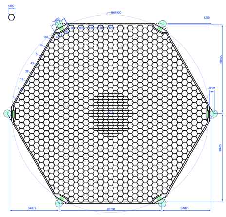
Based on the lab measurements[2] performed on the version 1 silicon sensor prototypes, we have developed a design for new (version 2) sensors which can be used to fabricate a full-depth (30-layer) ECal module. The new sensor design is depicted in Fig. 2. The layout minimizes capacitive and resistive noise contributions from the signal traces, especially in the vicinity of the KPiX chip. A typical trace contributes pF and .

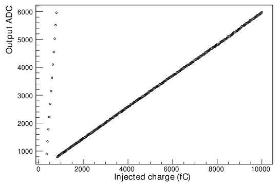
The readout of the Si pixels must accommodate a very large dynamic range. Based on EGS4 simulations, the largest signals in a single pixel—arising from 500 GeV Bhabha electrons—correspond to about 2000 MIPs at shower max. At the low end, one requires measuring MIPs well above the elcetronic noise (SNR or better). The KPiX design incorporates this large dynamic range in a novel way, using on-the-fly range switching. Figure 3 shows this range-switching function in action in the lab. In the plot, as the injected charge is increased, we see the range switch at about 700 fC. For 320 micron silicon, 1 MIP is equivalent to about 4.1 fC. Thus the upper end of the plot corresponds to about 2500 MIPs, more than the expected maximum.

If the KPiX heat load is kept below about 40 mW, the temperature gradient across an ECal module ( cm) can be kept at an acceptable level ( C) using only passive heat conduction via the tungsten radiators. Clearly, this is desirable, and is achievable by taking advantage of the beam-timing structure of the ILC, where beams are only present for 1 ms out of each 200 ms cycle. By cycling off most of the (analog) KPiX power between beam-crossing times, lab measurements of the prototypes confirm that the heat load of the full KPiX chip will be about 20 mW. This heat is to be passively conducted to the module edges behind the ECal (see Fig. 1), where it can be extracted.
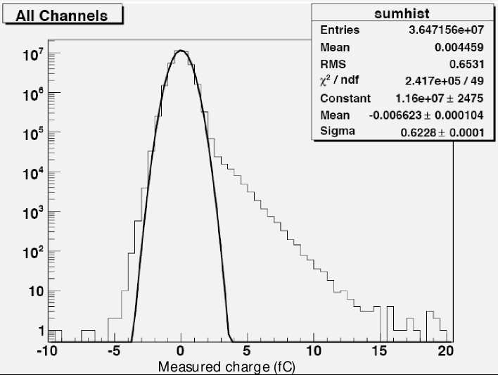
Recently, a KPiX v4 prototype was connected to a spare CDF silicon-strip detector and placed in a test beam at the SLAC End Station A (ESA). The data set is still being analyzed. A preliminary result is given in Fig. 4, which shows the detected charge distribution. Since the beam rate averaged electron per pulse, and the beam diameter was much larger than the active detector region, the distribution is dominated by the electronic noise, which is gaussian over several orders of magnitude. The single-MIP contribution is clearly visible.

References
-
[1]
Slides:
http://ilcagenda.linearcollider.org/contributionDisplay.py?contribId=389&sessionId=108&confId=1296 -
[2]
D. Strom et al.,
Proc. LCWS 2005, Stanford, California, 18-22 Mar 2005, pp 0908;
http://www.slac.stanford.edu/econf/C050318/papers/0908.PDF.