Mechanisms of exchange bias with multiferroic BiFeO3 epitaxial thin films
Abstract
We have combined neutron scattering and piezoresponse force microscopy to study the relation between the exchange bias observed in CoFeB/BiFeO3 heterostructures and the multiferroic domain structure of the BiFeO3 films. We show that the exchange field scales with the inverse of the ferroelectric and antiferromagnetic domain size, as expected from Malozemoff’s model of exchange bias extended to multiferroics. Accordingly, polarized neutron reflectometry reveals the presence of uncompensated spins in the BiFeO3 film at the interface with the CoFeB. In view of these results we discuss possible strategies to switch the magnetization of a ferromagnet by an electric field using BiFeO3.
pacs:
75.50.Ee, 77.80.-e, 75.70.Cn, 75.70.KwThe renaissance of multiferroics Spaldin and Fiebig (2005); Eerenstein et al. (2006), i.e. materials in which at least two ferroic or antiferroic orders coexist, is motivated by fundamental aspects as well as their possible application in spintronics Bibes and Barthélémy (2007). Such compounds are rare and the very few that possess simultaneously a finite magnetization and polarization usually order below about 100K Kato and Iida (1982); Yamasaki et al. (2006); Gajek et al. (2007). Ferroelectric antiferromagnets (FEAF) are less scarce, and some exhibit a coupling between their two order parameters. This magnetoelectric (ME) coupling allows the reversal of the ferroelectric (FE) polarization by a magnetic field Kimura et al. (2003) or the control of the magnetic order parameter by an electric field Zhao et al. (2006).
The practical interest of conventional antiferromagnets (AF) is mainly for exchange bias in spin-valve structures. The phenomenon of exchange bias (EB) W.H. Meiklejohn and C.P. Bean (1956) manifests itself by a shift in the hysteresis loop of a ferromagnet (FM) in contact with an AF and arises from the exchange coupling at the FM/AF interface Nogués and I.K. Schuller (1999); Radu and Zabel . Combining this effect with the ME coupling in a FEAF/FM bilayer can allow the reversal of the FM magnetization via the application of an electric field through the FEAF, as reported recently at 2K in YMnO3/NiFe structures Laukhin et al. (2006).
To exploit these functionalities in devices one needs to resort to FEAF materials with high transition temperatures. BiFeO3 (BFO) is a FE perovskite with a Curie temperature of 1043K J.R. Teague et al. (1970) that orders antiferromagnetically below TN=643K (TN: Néel temperature) S.V. Kiselev et al. (1963). BFO thin films have a very low magnetization (0.01 /Fe) compatible with an AF order Béa et al. (2005, 2006a), and remarkable FE properties with polarization values up to 100 C.cm-2 range Lebeugle et al. (2007). Recently, we reported that BFO films can be used to induce an EB on adjacent CoFeB layers at room temperature Béa et al. (2006b). This observation together with the demonstration of a coupling between the AF and FE domains Zhao et al. (2006) paves the way towards the room-temperature electrical control of magnetization with BFO. However, several questions remain before this can be achieved. Key issues concern the precise magnetic structure of BFO thin films, and the mechanisms of EB in BFO-based heterostructures.
In this Letter, we report on the determination of the magnetic structure of BFO films by means of neutron diffraction (ND), and the analysis of the EB effect in CoFeB/BFO heterostructures in terms of Malozemoff’s model A.P. Malozemoff (1987). Accordingly, we find a clear dependence of the amplitude of the exchange field HE with the size of the multiferroic domains, which provides a handle to control the magnetization of the CoFeB film by an electric field. The observation of EB and enhanced coercivity correlates with the presence of uncompensated spins at the interface between the FM and the AF, as detected by polarized neutron reflectometry (PNR).
BiFeO3 films were grown by pulsed laser deposition Béa et al. (2005), directly onto (001)- or (111)-oriented SrTiO3 (STO) or (001)-oriented LaAlO3 (LAO) substrates, or onto 10-25 nm-thick metallic buffers of La2/3Sr1/3MnO3 (LSMO) or SrRuO3 (SRO) Béa et al. (2006c). 7.5 nm-thick CoFeB layers were sputtered in a separate chamber at 300K in a magnetic field of 200 Oe, after a short plasma cleaning. The samples were capped by 10-30 nm of Au. High resolution x-ray diffraction evidenced a cube-on-cube growth for all the perovskite layers onto the substrates. CoFeB was amorphous. While the (111)-oriented films were found to be rhombohedral as bulk BFO Béa et al. , (001)-oriented films were found tetragonal or monoclinic Béa et al. (2007).
A first key information that is usually required to analyze EB is the magnetic structure of the AF. Bulk BFO is known to have a G-type AF order S.V. Kiselev et al. (1963), with a superimposed cycloidal modulation Sosnowksa et al. (1982). In view of the strong strain sensitivity of the properties of FE and magnetic oxides, one can anticipate that the magnetic order of BFO films might be different from that of the bulk. In order to determine their magnetic structure, selected (001)- and (111)-oriented BFO films were thus characterized by ND with the triple axis 4F1 spectrometer at the Orphée reactor of the Laboratoire Léon Brillouin (LLB) Béa et al. .
In a G-type AF, superstructure peaks are expected to appear at [½ ½ ½]-type reflections. In Fig. 1a and b, we show the diffracted intensity at the [½ ½ ½] reflection in BFO films grown on (001)- and (111)-oriented STO. Clearly an AF peak is present for both films. On the other hand, no intensity was measured at [0 0 ½]-type or [½ ½ 0]-type reflections, characteristic of A-type and C-type antiferromagnetism, respectively. These data thus show that both (001)- and (111)-oriented films are antiferromagnetic with a G-type order similar to that of the bulk. In other words, neither strain nor changes in the unit-cell symmetry modify the type of magnetic order, besides destroying the cycloidal modulation (see Ref. Béa et al., 2007 for details on this aspect).
Within a simplistic model of EB, the exchange field HE depends on the interface coupling Jeb= (Jex is the exchange parameter, SF and SAF are the spin of the interfacial atoms in the ferromagnet and the AF, respectively, and is the unit cell parameter of the AF), on the magnetization and thickness of the ferromagnet MFM and tFM, and on the anisotropy and the thickness of the AF KAF and tAF Radu and Zabel .
| (1) |
provided that 1/ is smaller than 1 (otherwise HE is zero). If tAF is large, and thus H. In a naive picture of perfect surfaces and because the AF order is G-type in both (001) and (111) films, the (111) films are expected to have magnetically uncompensated surfaces, yielding SAF=5/2, while the (001) films should have compensated surfaces, yielding in average SAF=0. Therefore, a finite HE should be found for (111) films only. For (111) films, taking Jex=5 10-22 J Ruette et al. (2004), a=3.96 , SF=1/2, SAF=5/2, MFM=800 kA/m and tFM=7.5 nm one can estimate Jeb=4 mJ/m2 and the large value of HE=6.5 kOe.
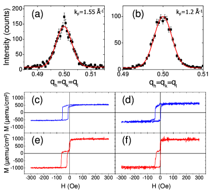
Figure 1c and d show M(H) hysteresis loops measured at 300K for BFO(70nm)/CoFeB stacks grown on STO(001) and STO(111). The loops are shifted towards negative magnetic field values by an exchange field HE of -39 Oe for (001) films and -19 Oe for (111) films. Furthermore the loops are enlarged by some tens of Oe compared to those measured on CoFeB single films Béa et al. (2006b). From M(H) data for LSMO/BFO/CoFeB samples (see Fig. 1e and f), a symmetric (i.e. not showing EB) contribution from the LSMO films is visible (the Curie temperature of our LSMO films is about 330K) in addition to that coming from the CoFeB. For a given thickness, the exchange field experienced by the CoFeB is virtually the same irrespective of the presence of the LSMO buffer layer.
Malozemoff’s random field model A.P. Malozemoff (1987) has been proposed to resolve the long-standing discrepancy between the model of Eq.(1) and the experimental data Nogués and I.K. Schuller (1999). It considers that in the presence of some atomic-scale disorder that locally creates a net magnetization in the AF at the interface with the FM, the AF splits into domains, which decreases considerably the interface coupling that now writes:
| (2) |
L is the antiferromagnetic domain size and a factor depending on the shape of the domains and on the average number of frustrated interaction paths for each uncompensated surface spin A.P. Malozemoff (1987). For hemispherical bubble domains, and is of order unity A.P. Malozemoff (1987). From equations (1) and (2) and for large AF thickness () the exchange field should vary as :
| (3) |
and indeed, a linear dependence of HE with 1/L was experimentally observed in several AF/FM systems Takano et al. (1998); Scholl et al. (2004), providing strong support to the model.
In order to determine the domain size in antiferromagnets, a technique of choice is X-ray photoelectron emission microscopy Stöhr et al. (1999); Scholl et al. (2000). Alternatively, an estimation of the average domain size can be inferred from the width of the ND peaks that reflects the coherence length in the sample J.A. Borchers et al. (2000). In some multiferroics like BFO, the FE and AF domains are coupled Zhao et al. (2006) so that it is possible to infer the size and distribution of the AF domains by imaging the FE domains, e.g. using piezoresponse force microscopy (PFM).
We have characterized the FE domains in two sets of BFO samples by combining in-plane and out-of-plane PFM measurements Catalan et al. . A first set consists of 65 nm-thick BFO films grown on different buffers and substrates (see table 1). A second set consists of BFO films with varying thickness (5 nm 240 nm) grown on LSMO//STO(001). In BFO, since the polarization is oriented along the 111 directions there generally exist 8 possible polarization orientation variants. This leads to a large number of possible domain patterns and to several types of domain walls (DWs) depending on the angle between the polarization vectors in the adjacent domains (71, 109 or 180∘). In principle only 71∘ and 109∘ FE DWs correspond to an AF DW Zhao et al. (2006). In most of the samples considered in this study, the three types of DWs are present, with the density of 180∘ type DWs being negligible.
In the following we analyze the exchange field in terms of the average FE domain size LFE that we identify to half the FE domain periodicity, and the average AF domain size LAF that we identify to the coherence length in the ND experiments. Even in the case of a strict correspondence between the FE and AF domains, LFE is expected to be larger than LAF because it comprises both the domain and the DW widths while LAF mostly reflects the domain width.
| Substrate | Buffer | (nm) | HE | LFE(nm) |
| STO(001) | LSMO | 70 | -39 | 58 |
| STO(001) | SRO | 70 | -14.5 | 98 |
| STO(111) | LSMO | 70 | -19 | 68 |
| STO(111) | SRO | 70 | -39 | 48 |
| LAO(001) | LSMO | 60 | 0 | 350 |
| LAO(001) | SRO | 60 | -29 | 55 |
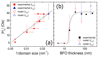
Let us first compare the values of LAF and LFE for the samples of Fig. 1. From Fig. 1a we calculate LAF=42 nm while from PFM we find LFE=58 nm for this sample. For the sample of Fig. 1b, LAF=56 nm and LFE=98 nm. LFE is larger than LAF by some tens of nm that likely correspond to the DW width DWwidth . When LAF increases LFE increases also, as expected if the AF and FE domains are correlated, as found by Zhao et al Zhao et al. (2006).
In figure 2a we plot the exchange field as a function of the inverse of the domain size for the first set of samples (constant thickness). A linear variation of HE with is observed, as expected from Eq. (3). Furthermore, there is an excellent quantitative agreement between the model and the data as illustrated by the similarity between the experimental points (solid symbols in Fig. 2a) and the values of HE calculated using the domain sizes (open symbols; the only free parameter is that we set to 3.2).
As illustrated by Fig. 2b, this model also accounts for the thickness dependence of the exchange field. Below a critical BFO thickness of about 10 nm, there is no exchange bias but at larger thickness, HE increases abruptly and takes values of about 40 Oe for t nm. A similar thickness dependence was reported for other AF/FM systems such as FeMn/NiFe Jungblut et al. (1994) and is expected from Eq. (1). Combining Eq. (1) and Eq. (2), and using the measured domain sizes one can calculate HE for these films. The only free parameters are and KAF. As shown by the open symbols in Fig. 2b, a rather good agreement with the data is obtained for =3.2 (as before) and KAF=6.8 kJ/m3. We note that this value of KAF is lower than the value inferred for the bulk from electron spin resonance experiments Ruette et al. (2004) by about one order of magnitude. This can be due to the low thickness of the BFO films and possibly to strain effects, or reflect modified magnetic properties at the BFO/CoFeB interface, as will be discussed in the following.
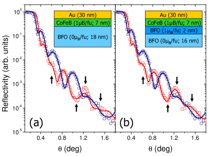
To validate the analysis of our data with Malozemoff’s model, we have attempted to detect the presence of a net magnetization in BFO close to the interface with CoFeB using PNR. The PNR measurements were carried out with the PRISM instrument of the LLB at room temperature. Spin-up and spin-down reflectivities (R++ and R–) were collected and the data were corrected for the polarization efficiency. The least square fittings were made using the Simul-Reflec software. The structural parameters of the layers were first determined by fitting X-ray reflectometry data (not shown). In the following we discuss the results for a Au(30nm)/CoFeB(7.5nm)/BFO(18nm)//STO(001) sample displaying an EB of 18 Oe and in which the CoFeB/BFO interface has a roughness of only 0.5 nm, yielding high quality reflectivity data.
Figure 3 shows the PNR results and the corresponding fits using two different sample models. In the first sample model (Fig. 3a) we only consider the presence of three layers, i.e. Au, CoFeB and BFO. The best fit is obtained for the structure Au(31.0nm)/CoFeB(7.0nm)/BFO(18nm) with zero magnetization in the BFO and Au layers, and a magnetization of 1 /f.u. for the CoFeB. As can be appreciated, the fit is good but not perfect (see arrows). The fit quality is significantly improved, especially at high , by using a four-layer model, i.e. splitting the BFO layer in two. The best fit is then obtained if a 2nm layer carrying a magnetic moment of 1/f.u. is present in the BFO, at the interface with the CoFeB. This ultrathin magnetic layer inside the BFO accounts for the presence of a large density of uncompensated spins (corresponding to a surface moment ms=31.8 .nm-2) at the BFO/CoFeB interface, similarly to results reported on the Co/LaFeO3 exchange bias system Hoffmann et al. (2002).
The expected surface moment due to pinned uncompensated spins within Malozemoff’s model is m=2SAF/aL0.32 .nm-2, which represents only a small fraction of the surface moment measured by PNR. The majority of uncompensated spins is thus unpinned (as observed by X-ray magnetic circular dichroism in Co/IrMn Ohldag et al. (2003)) and rotates with the CoFeB, producing an increase of the coercive field, as found experimentally (see Fig. 1). This observation suggests that two different, yet possibly related and complementary, strategies are possible to tune the magnetic switching fields of the ferromagnet electrically. One would rely on the manipulation of the pinned uncompensated spins to modify the exchange field HE, e.g. by changing the domain size that should be controllable by ad-hoc electrical writing procedures. The other could consist in controlling the unpinned uncompensated spins in order to alter the coercive field HC. This might be achieved by modifying the effective surface anisotropy of the AF, for instance by playing with the ferroelastic energy of the domains, which would change the magnetoelastic contribution to the anisotropy.
In summary, we analyzed the exchange bias in the CoFeB/BiFeO3 system and found that the exchange field does not correlate with the type of magnetic surface of the antiferromagnet - compensated or uncompensated. Rather, the exchange field scales with the inverse of the ferroelectric and antiferromagnetic domain size in the multiferroic BiFeO3 film, as expected from Malozemoff’s model that we extend for the first time to the case of ferroelectric antiferromagnets. Polarized neutron reflectometry measurements reveal the presence of a net magnetic moment within a 2 nm slab in the BFO at the interface with the CoFeB, reflecting the presence of uncompensated spins in the BiFeO3, consistent with the observation of exchange bias and enhanced coercivity. As the ferroelectric domain structure can be easily controlled by an electric field, our results strongly suggest that the electrical manipulation of magnetization should be feasible at room temperature in BFO-based exchange-bias heterostructures.
Acknowledgment
This study was supported by the E.U. STREP MACOMUFI (033221), the contract FEMMES of the Agence Nationale pour la Recherche. H.B. also acknowledges financial support from the Conseil Général de l’Essone. The authors would like to thank H. Jaffrès, M. Viret, G. Catalan and J. Scott for fruitful discussions.
References
- Spaldin and Fiebig (2005) N. Spaldin and M. Fiebig, Science 309, 391 (2005).
- Eerenstein et al. (2006) W. Eerenstein, N.D. Mathur, and J.F. Scott, Nature 442, 759 (2006).
- Bibes and Barthélémy (2007) M. Bibes and A. Barthélémy, IEEE Trans. Electron Dev. 54, 1003 (2007).
- Kato and Iida (1982) K. Kato and S. Iida, J. Phys. Soc. Jpn. 51, 1335 (1982).
- Yamasaki et al. (2006) Y. Yamasaki et al., Phys. Rev. Lett. 96, 207204 (2006).
- Gajek et al. (2007) M. Gajek et al., Nature Materials 6, 296 (2007).
- Kimura et al. (2003) T. Kimura et al., Nature 426, 55 (2003).
- Zhao et al. (2006) T. Zhao et al., Nature Materials 5, 823 (2006).
- W.H. Meiklejohn and C.P. Bean (1956) W.H. Meiklejohn and C.P. Bean, Phys. Rev. 102, 1413 (1956).
- Nogués and I.K. Schuller (1999) J. Nogués and I.K. Schuller, J. Magn. Magn. Mater 192, 203 (1999).
- (11) F. Radu and H. Zabel, cond-mat.mtrl-sci/0705.2055.
- Laukhin et al. (2006) V. Laukhin et al., Phys. Rev. Lett. 97, 227201 (2006).
- J.R. Teague et al. (1970) J.R. Teague, R. Gerson, and W.J. James, Solid State Commun. 8, 1073 (1970).
- S.V. Kiselev et al. (1963) S.V. Kiselev, R.P. Ozerov, and G.S. Zhdanov, Sov. Phys. Dokl. 7, 742 (1963).
- Béa et al. (2005) H. Béa et al., Appl. Phys. Lett. 87, 072508 (2005).
- Béa et al. (2006a) H. Béa et al., Phys. Rev. B 74, 020101(R) (2006a).
- Lebeugle et al. (2007) D. Lebeugle, D. Colson, A. Forget, and M. Viret, Appl. Phys. Lett. 91, 022907 (2007).
- Béa et al. (2006b) H. Béa et al., Appl. Phys. Lett. 89, 242114 (2006b).
- A.P. Malozemoff (1987) A.P. Malozemoff, Phys. Rev. B 35, 3679 (1987).
- Béa et al. (2006c) H. Béa et al., Appl. Phys. Lett. 88, 062502 (2006c).
- (21) H. Béa et al., unpublished.
- Béa et al. (2007) H. Béa, M. Bibes, S. Petit, J. Kreisel, and A. Barthélémy, Philos. Mag. Lett. 87, 167 (2007).
- Sosnowksa et al. (1982) I. Sosnowksa, T. Peterlin-Neumaier, and E. Steichele, J. Phys. C 15, 4835 (1982).
- Ruette et al. (2004) B. Ruette et al., Phys. Rev. B 69, 064114 (2004).
- Takano et al. (1998) K. Takano, R.H. Kodama, A.E. Berkowitz, W. Cao, and G. Thomas, Phys. Rev. Lett. 79, 1130 (1998).
- Scholl et al. (2004) A. Scholl et al., Appl. Phys. Lett. 85, 4085 (2004).
- Stöhr et al. (1999) J. Stöhr et al., Phys. Rev. Lett. 83, 1862 (1999).
- Scholl et al. (2000) A. Scholl et al., Science 287, 1014 (2000).
- J.A. Borchers et al. (2000) J.A. Borchers et al., Appl. Phys. Lett. 77, 4187 (2000).
- (30) G. Catalan et al., cond-mat.mtrl-sci/0707.0371.
- (31) The domain wall width in BiFeO3 will be discussed in a separate paper.
- Jungblut et al. (1994) R. Jungblut et al., J. Appl. Phys. 75, 6659 (1994).
- Hoffmann et al. (2002) A. Hoffmann et al., Phys. Rev. B 66, 220406(R) (2002).
- Ohldag et al. (2003) H. Ohldag et al., Phys. Rev. Lett. 91, 017203 (2003).