FANO RESONANCES IN STUBBED QUANTUM
WAVEGUIDES WITH IMPURITIES
Abstract
We consider T–shaped, two–dimensional quantum waveguides containing attractive or repulsive impurities with a smooth, realistic shape, and study how the resonance behavior of the total conductance depends upon the strength of the defect potential and the geometry of the device. The resonance parameters are determined locating the relevant –matrix poles in the Riemann energy surface. The total scattering operator is obtained from the –matrices of the various constituent segments of the device through the –product composition rule. This allows for a numerically stable evaluation of the scattering matrix and of the resonance parameters.
pacs:
73.63.Nm Quantum wires, 73.23.Ad Ballistic transport, 72.10.Fk Scattering by point defects, dislocations, surfaces, and other imperfections (including Kondo effect)Preprint DFPD/07/TH11
I Introduction
The discovery of conductance quantization in microcostrictions wee88 ; wha88 has prompted a great deal of theoretical and experimental activity on electron transport in such systems da95 ; fg99 ; lo99 . It has been soon realized that the presence of an impurity in the waveguide can modify the shape of the conductance dramatically, especially near the thresholds where propagation modes are opened. These effects have been investigated in many model calculations, for both point–like defects bag90 ; kcb96 ; blr00 ; blr00p and more realistic, finite–range defect shapes bag90 ; kis99 ; bam04 ; vap05 . The scattering of the electron wave off the impurity produces resonance phenomena in the conductance; in particular, for attractive impurities one has deep transmission minima, which can be interpreted as due to the coupling of a propagation mode in one subbband with a localized state formed from another subband. This resonant suppression of ballistic conductance is similar to the Fano resonances one observes in atomic and nuclear physics, and has been the subject of detailed numerical kis99 ; bam04 ; vap05 and theoretical gl93 ; ns94 investigations. Needless to say, whereas theoretical arguments can give insight into the general mechanisms underlying the formation of resonances, only detailed numerical experiments can provide information about the dependence of resonance parameters upon the strength, shape, and position of the impurity potential inside the quantum waveguide.
The step–wise structure of conductance can be deeply influenced also when the waveguide boundary is modified, with respect to an idealized, straight shape. In particular, the effects of a sidearm, or stub, attached to the duct have been the subject of several investigations mak91 ; wus91 ; shx96 ; sh97 ; der00 ; wv02 ; wrb05 since the pioneering papers of Sols et al. som89 ; som89l , where a T–shaped waveguide was considered as a possible candidate for transistor action based on quantum interference. The conductance as a function of the Fermi energy exhibits deep transmission minima, which can be again interpreted as reflection resonances due to the excitation of quasi–bound states in the cavity region der00 . A great deal of theoretical activity has been devoted to disentangle the physical factors influencing Fano line shapes in these mesoscopic systems. Indeed, Fano resonances are interesting in themselves, because they are extremely sensitive to the details of the scattering process, and may be exploited to probe the degree of coherence in the scattering device getal00 ; cwb01 ; rl04 ; umm07 ; at the same time, their strong dependence upon the energy of the scattered particle make them promising candidates for practical applications, such as the spin filtering action when spin degeneracy is removed by the application of an external magnetic field or by use of the Rashba effect sob03 . At low level densities, and for systems coupled to very few channels, quantum interference between quantum states plays a prominent role, and a detailed quantum-mechanical study of the scattering device is required. The dependence of the spectral properties of quantum dots attached to quantum waveguides upon the dot’s dimensions has been the subject of detailed analysis in recent years nr98 ; sbr06 .
To the best of our knowledge, up to now an analysis of the simultaneous effects of impurities and stubs in quantum interference devices has never been accomplished. It is the purpose of this paper to provide a first contribution, in order to fill this gap. In particular, we have studied how the resonance features of the conductance depend upon the strength of an embedded defect, and the size of the stub. To this end, we have determined how the resonance poles of the scattering operator for the device move on the multi–sheeted Riemann energy surface, as the device parameters are varied. For stubbed waveguides with realistic defects, this requires an accurate numerical solution of the two–dimensional Schrödinger equation, in a large range of values for the stub’s dimensions. This is made possible combining mode–matching techniques with an –matrix approach. The device is regarded as a cascade of uniform waveguide sections, connected through interfaces or junctions, where a change in the transverse dimensions occurs, or the electron experiences a variation in the strength of the interaction. The scattering parameters of the device can be then determined starting from the scattering properties of the various building blocks through the –product composition rule for the partial scattering operators da95 ; ki88 ; cm88 . Since forward and backward states are treated separately by the –matrix, so that the propagating and less localized components play a prominent role, numerical stability is guaranteed as some dimension of the system becomes large. At the same time, a varying number of basis functions can be accommodated in a natural way in the scattering matrix approach; this is particularly important in non–uniform waveguides, where one expects that a different number of wave–function components has to be considered as the transverse size of the device changes. Thus, the employment of the scattering operator, together with the –product composition rule, opens the way to an accurate description of devices with a fairly large number of different constituent segments, as required when dealing with impurities having a smooth profile along the propagation direction. They are in fact approximated by a cascade of several thin layers, in which the dependence upon the propagation coordinate is neglected.
The paper is organized as follows. In Sect. II we review the scattering matrix approach to ballistic transport in quantum waveguides. In particular, we point out the compatibility between the –product composition rule and the non–trivial block–wise structure of the partial –matrices, when a different number of basis functions is chosen in different slices of the device. With reference to this point, we would like to point out that, whereas the numerical stability of the –matrix has been widely recognized in the literature da95 ; ki88 , its flexibility with respect to the number of wave function components has been less stressed in the past, with the exception of Ref. wei91 . In Sect. III we give several examples of how the device parameters influence the pole location in the energy–plane, and how this affects the resonant behavior of the conductance. Our main conclusions are briefly summarized in Sect. IV.
II Scattering formalism for quantum transport in stubbed waveguides
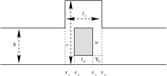
We consider the T–shaped device illustrated in Fig. 1. It consists of a uniform guide of indefinite length and width , with a sidearm (stub) having width and length . We shall assume simple hard wall boundary conditions, so that the two–dimensional electron wave function has to vanish on the boundary of the device. The stub may contain a region, where there is a defect, or an external applied field. This region, to which we shall simply refer as “defect”, is exhibited by the shaded area in Fig. 1. The electron’s wave function is then the solution of the two–dimensional Schrödinger equation for a given total energy , the electron in the conduction band being endowed with an effective mass . In the present paper we have chosen for the value , which is appropriate for the interface. The potential field due to the defect will be represented by an interaction term , whereas the effect of the confining potential is taken into account through the boundary conditions that vanishes along the edge of the straight duct and of the stub.
Because of the presence of the potential term , the full Schrödinger equation is not in general separable. As is well known lo99 , one can reduce it to an (in principle) infinite set of one–dimensional differential equations by expanding its solution into the transverse mode eigenfunctions in the leads and in the stub . Under the assumption of hard-wall boundary conditions, these basis functions are just the eigenfunctions of infinite square wells in the transverse direction, with widths and in the leads and in the stub, respectively.
The whole device can be divided into five regions; the left and right ducts, the two empty cavities in the sidearm, and the defect. The total wave function in the different regions of the stub can be piecewise expanded in terms of the basis functions . Once this expansion is inserted into the Schrödinger equation, one immediately finds that the expansion coefficients satisfy uncoupled differential equations, and can be written in terms of forward and backward propagating waves in the regions of the stub where the potential is negligible; the corresponding wave numbers are related to the total energy and to the transverse eigenenergies by
| (1) |
These relations essentially express the conservation of energy; once the –th transverse eigenmode has been excited, only the energy is left for the electron propagation along the –direction. If , the wave number has to be taken as purely imaginary, i.e., , with
| (2) |
The associated propagating waves become then real, exponentially decaying or growing wave functions, and one has an evanescent mode, or closed channel.
In presence of the defect a somewhat more involved procedure is required, since one gets coupled equations for the expansion coefficients. These equations can be straightforwardly uncoupled, and the coefficients written in terms of forward and backward propagating waves, if one assumes for the potential the simple form
| (3) |
where is the Heaviside step function. In such a case one arrives at the required result diagonalizing the Hamiltonian for the transverse motion, in the model space spanned by the basis functions bag90 . In the potential region of the stub the expansion coefficients can then be written as linear superpositions of plane–wave components , with wave vectors
| (4) |
the quantities being the eigenvalues of the transverse Hamiltonian. Here also, if , the wave number is purely imaginary, in completely analogy to Eq. (2), and one has evanescent, non propagating modes in presence of the defect interaction.
Similar considerations can be repeated for the wave function in the leads, the only difference being that now the transverse eigenmodes have to be used. The wave vectors in the leads are given by expressions quite similar to Eqs. (1) and (2) for open and closed channels, respectively, with the stub transverse eigenenergies replaced by the lead corresponding quantities . For the time being, we shall not specify the actual boundary conditions the wave function has to satisfy asymptotically, and we let the presence of incoming and outgoing waves from both the left and from the right in the ducts. We just limit ourselves to observe that, in correspondence to closed channels, one must exclude incoming waves from the left or from the right, in order to avoid divergent components in the wave function.
The unknown coefficients appearing in the expansion of the wave function in the various regions can be related to one another by matching the wave function and its first derivative at the various interfaces. The linear transformation yielding the coefficients on one side of an interface in terms of those on the other side represents what is usually referred to as the transfer matrix lo99 . It is well–known that the transfer matrix suffers from several limitations ki88 ; xu94 . First of all, its generalization to the case where there is a different number of basis functions on the left of the matching surface with respect to the right is not straightforward. This is particularly relevant at the lead/stub or stub/lead interfaces, where a different number of open and closed channels may occur in the cavity with respect to the lead. A second problem arises in presence of evanescent modes, whose occurrence makes the inversion of the transfer matrix numerically troublesome when one evaluates the transmission coefficients as the dimensions of the device get large. The above shortcomings can be all overcome resorting to the scattering matrix da95 ; fg99 . In such a case, one expresses the outgoing amplitudes in terms of the incoming ones, to get
| (5) |
where the sub-matrices are given by
| (6a) | |||||
| (6b) | |||||
| (6c) | |||||
| (6d) | |||||
with
| (7a) | |||||
| (7b) | |||||
The actual structure of the matrices and depends upon the matching conditions one is considering. Whatsoever these conditions may be, one does not need to assume the same number of basis functions on the two sides of the matching surface, since the building blocks of the total -matrix are not required to be square. As a matter of fact, if wave function components are retained on the left, whereas basis functions are considered on the right, the whole sub-matrix has dimensions , and is a square array, whereas and have dimensions and , respectively. Overall, the total -matrix expresses the outgoing amplitudes in terms of the coefficients of the incoming waves. As for the diagonal matrix , it takes into account the propagation of the wave function in the slice on the left of the matching surface, and is defined according to
| (8) |
where is the width of the slice, and are the corresponding propagation wave numbers. It is worth to observe that in the scattering matrix only the phase factors appear. In correspondence to an evanescent mode, one actually has the exponentially decaying factors , which are no longer mixed up with the growing functions . As the numerical calculations confirm, these features make the whole formalism numerically stable even when some characteristic length of the system, and in particular the stub’s width , gets large.
Finally, we give the actual structure of the matrices and at the lead/stub and cavity/defect interfaces. For the former one has , , and , . The matrix contains the overlap integrals among the different basis functions on the left and on the right of the discontinuity,
| (9) |
is the transpose of , while and are and diagonal matrices, whose diagonal elements represent the wave vectors and , in the lead and in the stub, respectively. For the cavity/defect interface, on the other hand, one has , , and , , where is the matrix diagonalizing the transverse Hamiltonian in the interaction region, and the diagonal matrix contains the wave vectors defined by Eq. (4). For the sake of simplicity, we have assumed an equal number of basis functions on the left and on the right of the cavity/defect boundary; as a matter of fact, the potential in general is not so strong, as to perturb the transverse eigenvalues in an essential way, and good convergence can be achieved with an equal number of wave function components outside and inside the defect.
The unperturbed propagation along the slice preceding the interface can be put in better evidence by re-writing Eq. (5) as a suitable combination of elementary scattering operators. This can be achieved through the –product of –matrices da95 ; ki88 ; cm88 , which expresses the overall scattering matrix in terms of the partial scattering matrices and as
| (10) |
where
| (11a) | |||||
| (11b) | |||||
| (11c) | |||||
| (11d) | |||||
It is worth to observe that this composition rule does not require the sub-matrices and to be square matrices. In particular, the –matrix appearing in Eq. (5) can be factorized as follows
| (12) |
where the block–wise anti–diagonal factor takes into account the free propagation through the slice on the left of the interface, and the reduced –matrix exhibits the effects on the wave function of the matching at the interface between the two considered regions of the device. The former is a matrix, whereas the latter has dimensions , as detailed above.
Eqs. (10) and (12) have been systematically employed to evaluate the total –matrix, starting from the partial –matrices at the lead/stub and cavity/defect boundaries, as well as from the scattering operators for the free propagation of the electron along the various slices of the device. As noted above, while there are physical reasons to choose a different number of transverse basis functions in the lead with respect to the sidearm, one can choose the same number of components in the empty slices of the stub and inside the defect. Thus, one has an partial –matrix at the lead/stub boundary, and a partial –matrix for the cavity/defect propagation. One can verify by inspection that, when the two operators are combined through the composition rule (10), one gets again a matrix with dimensions . Things are a bit different when one considers the stub/lead interface on the right of the device. We shall not enter here into the detailed structure of the stub/lead interface –matrix. We limit ourselves to note that, once the lead/stub –matrix has been evaluated, the corresponding –matrix on the right can be obtained without further computational effort, through the correspondence rule
| (13) |
A similar result holds for the –matrices at the cavity/defect and defect/cavity interfaces. As a consequence of Eq. (13), once the partial –matrix describing the propagation inside the device is combined with the –matrix through the -product composition rule (10), one gets an overall scattering operator , which effectively takes into account the flux percolation through open and closed channels in the sidearm.
Potentials having a non–trivial dependence can be accommodated in our approach through a slicing technique vap05 ; shx96 . This is particularly easy to do for interactions which are factorisable in their and dependence, such as the double Gaussian
| (14) |
If and are two points, where the value of the potential is negligible, we divide the interval into sub–intervals of equal width , and mimic the smooth potential by a sequence of pseudo–defects, each of width and strength
with . The conductance of the waveguide in presence of the smooth potential (14) is then evaluated for increasing , until convergence of the results is obtained.
Let us finally fix the actual boundary conditions under which we are solving the scattering problem. We shall assume that an electron impinges on the device moving from the left, with no flux coming from the right. If one assumes an incoming wave of unit flux in a given propagation mode, then the matrix elements represent the reflection coefficients toward the left from the initial channel into the final propagation mode , while the quantities give the transmission amplitudes to the right from mode into mode . Finally, for a two–probe device the total conductance can be evaluated through the Büttiker formula da95 ; fg99 ; bi85
| (15) |
where the summation is restricted to the open channels in the leads.
III Selected numerical examples
Our aim is to study the dependence of resonance parameters in a stubbed quantum wave guide upon the strength of an embedded defect and the geometry of the device, with particular reference to the stub height. We shall do this by locating the relevant S-matrix poles in the multi-sheeted energy plane, with cuts starting along the real axis from the various scattering thresholds. From now on, all lengths are measured in units of the waveguide width , and energies in terms of the waveguide’s fundamental mode , so that the various thresholds are . Sheets will be specified giving the sign of the imaginary part of the lead’s momenta in each channel lw67 . Thus, referring to a four–channel situation, the symbol denotes the physical sheet, where the imaginary parts of all the channel momenta are positive, whereas on sheet one has , and for the other three channels. Our calculations refer to a duct with a double Gaussian defect described by Eq. (14). In all cases we have chosen , and , so that the region where the potential acts has a length . Moreover, we have set ; for a wave guide of width Å , the interaction region is therefore Å wide and Å long. The defect is placed at from the lower edge of the guide. The decay constants along the transverse and the propagation direction have been fixed at and , respectively, so as to ensure that the potential is negligible outside the interaction region. We have checked the convergence of the slicing method, and found that quite stable results are obtained with sub–intervals.
For a waveguide attached to a stub of height and length , one can expect that a larger number of basis functions is required in the stub than in the guide to achieve convergence, this difference increasing with increasing . As a matter of fact, for a given electron’s energy there are less open channels in the waveguide than in the stub, the thresholds in the two regions being and , respectively. It follows that, for a given energy , the number of open channels in the stub scales as , whereas in the guide it scales as . Since a sensible calculation has to include at least all the propagating modes, a larger number of basis functions is required in the stubbed region. As for the evanescent modes, one may recall that a closed–channel component is the less effective the shorter its attenuation length shx96 . The attenuation lengths in the lead and in the cavity are given in terms of the total energy by
| (16) |
From Eqs. (16), one has that two evanescent modes and , in the external region and in the stub, respectively, have the same attenuation length if the corresponding quantum numbers are related by . As a consequence, if components are required in the lead, closed channels have to be included in the stub, to assure convergence. Our numerical results are consistent with these estimates for both the conductance and the pole locations in the complex energy plane. We have obtained stable results with four components in the lead, and basis functions in the stub for . In these conditions, the position of the resonance poles in the -plane can be guaranteed with an accuracy of the order . Only the bound–state poles turned out to be more sensitive to the number of employed basis functions in the interaction region, which was to be expected. In this latter case, we employed four channels in the duct and up to 20 modes in the internal region.
The conductance of stubbed waveguides is characterized by a more or less complex pattern of transmission maxima and minima when considered as a function of the electron’s energy. In Fig. 2 we give the conductance of a waveguide having , with a repulsive defect of strength , in the energy region corresponding to the first two subbands .

One notes two transmission zeros in the first subband, and a non-trivial oscillatory behavior with two large dips in the second one. We looked for poles of the –matrix in the unphysical sheets and and found two resonance poles at and on the former sheet, and two pairs of neighboring poles in the sheet. The value of their real parts is exhibited by the vertical dashed lines in Fig. 2. The two poles close to the first subband, together with the two transmission zeros, concur to produce the strong variations in the conductance one observes there. As for the poles on the sheet, the first pair corresponds to the two almost overlapping peaks one sees just above the lower edge of the second subband, whereas the other two poles give rise to the broad resonances at the top of this energy region. It is worth to note that the maxima of the conductance are not aligned with the pole positions, which are very close to the transmission zeros in the first subband. The conductance behavior in the lowest subband is consistent with what one observes in simple, single–channel models for stubbed waveguides, where transmission resonances arise because of the presence of zero–pole pairs in the complex energy plane spl94 . In the higher subband, one clearly has a strong coupling between the occurring resonances.
We have studied how the resonance poles move as the defect strength varies with respect to the unperturbed situation, with the interaction switched off. Limiting ourselves to the first subband, for the sake of simplicity, we give the outcome of our calculations in Fig. 3, for a stub of height and the strength varying in the interval . For each resonance pole in the fourth quadrant of the energy plane, one observes a complex conjugate pole in the first quadrant. This is a confirmation of the correctness of our calculations. Indeed, the multichannel –matrix, when regarded as a function of the channel momenta , has the basic property bk82 , which implies that to a pole located at there corresponds a pole at the complex conjugate energy .

As the defect strength becomes more and more repulsive, both resonance poles in the fourth quadrant move upwards in energy, starting from the empty-stub positions, marked by the full dots in Fig. 3. At the same time they move away from the real axis; the presence of a repulsive interaction displaces the resonance peaks at higher energy, as it was to be expected. The broadening of the resonances with increasing defect strength is consistent with the calculations of Ref. cwb01 , where the effects of an impurity near the opening of a quantum dot was considered, in an attempt to simulate the non-monotonic resonance width found in a previous experiment getal00 . This effect can be attributed to the deflection of more and more electrons into the dot, as increases, so that the coupling between the waveguide and the cavity gets stronger cwb01 . Stated in equivalent terms, one may say that the wave function trapping in the region where the waveguide and the duct match decreases at the defect becomes more repulsive. In the range of strengths we have explored , on the other hand, we found no evidence of a non-monotonic behavior of the resonance width. For the pole at higher energy moves above the upper edge of the first subband , and becomes a shadow pole et64 . As for the low–lying pole, we have pushed the strength up to , finding no signal of a decreasing width. The reason for this difference with respect to cwb01 can be traced back to the different role played by backscattering in the two cases. In Ref. cwb01 the impurity is near the opening of the dot, whereas in our case it is embedded in the lower half of the waveguide. The pole trajectories in the complex energy plane depend in a rather sensitive way upon the position of the defect in the device, as we have found in previous model calculations clp06 . If the defect is displaced closer to the dot, backscattering can have an increased role, and a non-monotonic behavior of the resonance width may emerge.
For negative strengths, the two poles become closer and closer to the real axis; the first pole touches the real axis at for , while the higher pole trajectory touches it at when . Within the accuracy of the numerical calculations, we found that each pole lies just on the real axis in these conditions, at energies in the continuum of the first transmission band. This is an indication that for and one has a bound state embedded in the continuum (BIC) in the first subband. For increasingly negative strengths, the –matrix poles move away again from the real energy axis. The behavior of the low-lying pole is particularly worth of attention. As the defect becomes more and more attractive, its trajectory bends towards the real axis, which is reached for , at . At this point, the complex conjugate pole coming from the first quadrant collides with the resonance pole, giving rise thereby to a double pole below the scattering threshold . What is happening can be most clearly perceived in the complex plane, as exemplified in Fig. 4. As the absolute value of the strength increases, the pole in the fourth quadrant of the momentum plane moves downwards towards the imaginary axis, the corresponding pole at in the third quadrant doing the same; the two poles collide at , when . Decreasing the strength further, one has two anti–bound–state poles, one moving downwards along the negative imaginary axis, the other moving upwards, until, for it crosses the real axis, and passes into the upper half of the complex –plane as a bound state pole. Had we looked at the corresponding poles in the energy plane, we would have seen two poles moving on the real axis on the unphysical sheet, one of the poles reaching the first scattering threshold , and going back as a bound–state pole on the physical sheet. This situation is strongly reminiscent of what happens in standard potential scattering theory, and has been found also in idealized, one–dimensional models of stubbed waveguides clp06 .

We have studied how the bound-state energy changes when the strength of the defect or the stub’s height varies. The possibility of bound–state solutions for an empty stub has been known since several years ago lo99 . For an empty stub, the increasing of has a binding effect, the binding energy becoming substantially independent upon the stub’s size for . This can be easily explained, since the bound-state wave function is mainly concentrated in the region where the duct matches the stub, and for large cavities a change in the transverse dimension cannot affect the wave function in a substantial way. When the interaction is switched on, one observes that the bound state appears for increasing values of for repulsive defects; for a given , the binding energy is shifted upwards. In correspondence to an attractive defect, the curve is shifted downwards, and a bound state is possible even for a smooth wave guide, when the potential is able to support a bound state by itself.
The asymmetric line shapes one observes in the conductance of quantum waveguides are generally parametrized in terms of the Fano function
where is the amplitude of the Fano resonance, represents the reduced energy, and the pole location in the energy plane has been written as . The Fano parameter is a measure of the ratio between the resonant and non–resonant transmission amplitudes, and is related to the asymmetry of the line shape. For strictly one–dimensional systems, can be evaluated starting from the positions and of the –matrix zeros and poles in the energy plane, i.e, psl93
| (17) |
Eq. 17 can be used in the present multi–channel situation below the second scattering threshold, since in the first subband only one propagation mode really contributes to the conductance. To this end we have studied how the zeros of the scattering amplitude move as the strength varies. As expected, as the interaction becomes more and more repulsive the zeros move towards the upper threshold, whereas they are displaced towards lower energies for more and more negative strengths. In Fig. 5 we plot the resulting parameter for the two resonances observed in the first subband, when the strength varies in the range and .

The Fano parameter of the low–lying resonance is always positive, whereas for the second resonance it turns out to be negative. This implies that the two line shapes have opposite asymmetries for all the considered strengths, as confirmed by the calculated conductance. In both cases the absolute value of the asymmetry parameter remains always different from zero, with a rather smooth dependence upon in a rather large range of strength values.

We have also studied how the position of the -matrix poles and zeros depends upon the stub’s height . The “binding” effect of an increasing observed for the bound–state energies is clearly perceivable in the scattering region also. As the stub becomes longer, poles and zeros move towards the lower edge of the first subband, the trajectories of the first and second pole moving away from the real axis for and , respectively. As is increased further, the two poles come closer and closer to the real axis, giving rise to narrower and narrower resonances, until they leave the scattering region. We looked for the possible presence of BICs with varying . No positive-energy states with a vanishing width emerged from our calculations, both in presence of an impurity and for an empty stub. BICs for various values of the total transverse width have been found on the other hand in Ref. sbr06 , for a quantum billiard with a transverse hyperbolic profile coupled symmetrically to a quantum waveguide. There, arguments have been also given in favor of a rather widespread presence of BICs in mesoscopic systems. The fact that such zero-width states do not appear in the present calculations in a rather large range of stub’s heights can be explained by the geometry we have chosen. Our stub represents a rather narrow resonator, with ; the quantum billiard considered in Ref. sbr06 , on the other hand, has and . The possible presence and location of BICs is strictly related to the cavity’s eigenenergies, whose values and spacings depend in a crucial way upon the cavity’s dimensions. As a matter of fact, we verified that for an empty stub symmetrically coupled to the leads, and of dimensions comparable to the quantum billiard of Ref. sbr06 there is a BIC at for , in remarkable agreement with sbr06 , given the different shape of the confining potential. We checked the effect of a host impurity on the presence and energy of BICs. To this end, we introduced a double–Gaussian defect centered in the cavity, having . We found that BICs are a rather “robust” feature of the system, since for the zero-width state survives the switching on the interaction. When the strength is increased up to , one has a BIC at a slightly higher energy , provided that the stub’s height is adjusted to , which means a variation of the order of . Bound states in the continuum may appear also in more complicated systems. Recently, they have been found for two open quantum dots, coupled through a connecting bridge onk06 . In this case also we verified that when the strength of a host interaction is increased from up to , the BIC survives, being slightly displaced upwards in energy, at price of a small adjustment in the neck’s length . More precisely, one has , for , and , for . Both for the single and the coupled quantum dots the underlying mechanism, as viewed in the complex energy plane, is the same; when the strength of the interaction changes, both the pole and the transmission zeros move away from their original positions and are shifted upwards in energy; since they move at different speeds, however, if they coincided for a given value of the strength, they do not coincide any longer for the new strength. Their relative position can be adjusted to zero by a change of some characteristic length of the system, so as to have a BIC at a somewhat higher energy.
In analogy with Fig. 5, in Fig. 6 we plot the Fano parameter (upper panel) and the width (lower panel) for the considered poles as functions of . Note that the parameter for the higher–energy resonance is not given for ; as a matter of fact, for stubs of smaller width, this zero-pole pair cannot develop any longer in the considered energy region. For stubs having one actually finds that the considered –matrix pole in the sheet is located above the scattering threshold , thereby becoming a shadow pole. The asymmetry parameters turns out to be rather sensitive functions of , and can change sign as varies in between and . As a consequence, one expects a rather marked variation in the dependence of conductance upon the energy for stubs of different width, an expectation which is confirmed by our calculations. The origin of Fano lineshape reversal has been studied in a model coupled-channel calculation in Ref. kms07 . There, the sign change of for the resonances appearing in the electron transmission spectrum of a quantum dot has been attributed to the coupling among shape and Feshbach resonances originating from open and closed channels; this effect turned out to be very sensitive to slight modifications of the quantum-dot geometry. A similar mechanism is presumably at work here, since as increases, the poles move in the energy plane and new propagating modes open up in the cavity region; as a consequence. with varying , the parameter of each resonance changes sign, and the Fano profiles one observes in the first subband may or may not have the same asymmetry, depending upon the stub’s height one is considering.
Finally, we observe that the analysis of the pole trajectories can be extended to the sheet, in correspondence to the second subband. Similarly to what has been found below the second threshold, one finds a strong repulsive effect with decreasing . Poles, determining a resonance behavior for a given , move up in energy until they cross the third threshold and become shadow poles; at the same time new poles may come into play, moving from lower energies.
IV Conclusions
We have studied the poles in the complex energy plane of the multi–channel –matrix for a waveguide attached to a resonant cavity. We have allowed for the presence of a defect in the waveguide. Our main aim was to to get a quantitative insight into the dependence of the resonance parameters upon the defect strength and stub’s height. We found that a decrease of the stub’s size as an increase of the positive strength has a repulsive effect on the poles, which move in both cases to higher energies in the –plane. In particular, as the stub gets shorter, the –matrix poles pass the upper edge of the considered subband, becoming thereby shadow poles; at the same time, poles at lower energies come up, cross the lower threshold of the subband, and are therefore able to influence the resonant behavior of the conductance. For attractive defects, poles in the first and fourth quadrant move towards the real axis as the strength is made more negative; with reference to the lowest energy region, there are indications that bound states embedded in the continuum occur for critical values of the strength. As the defect becomes more and more attractive, resonance and anti-resonance poles collide on the real axis, giving rise to anti-bound state poles moving on opposite directions, until a bound state pole appears on the physical sheet, in close analogy with what happens in one–dimensional models of stubbed waveguides clp06 . For repulsive defects, zero-width scattering states appear for both single and coupled quantum dots, provided that the resonating cavity has the proper geometry, and represent a “robust” phenomenon with respect to the presence of an embedded interaction.
For the lowest subband, where only one open channel contributes to the conductance, one can relate the parameters appearing in the Fano function for the line shape to the poles and zeros of the scattering amplitude in the energy plane. The asymmetry parameter turns out to be a rather smooth function of the strength, whereas it depends more sensitively upon the stub’s size, and may even change sign with varying . As a consequence, one may or may not observe a reversal of the Fano line shape for the resonances in the first subband, depending upon the value of the stub’s height.
Some issues deserve certainly further investigations. The role of shadow to dominant pole transitions in explaining the changes of the total conductance near thresholds as varies has been discussed elsewhere cl07 . There is evidence of strong resonance overlapping in higher subbands. A quantitative study of resonance coupling effects, and their dependence upon the dynamical and geometrical parameters of the quantum device can be performed resorting to modern effective–Hamiltonian techniques op03 , in analogy to what has been done for microwave billiards sto02 . These issues are currently under consideration.
References
- (1) B. J. van Wees, H. van Houven, C. W. J. Beenakker, J. G. Williamson, L. P. Kouwenhoven, D. van der Marel, and C. T. Foxon, Phys. Rev. Lett., 60, 848 (1988).
- (2) D. A. Wharam, T. J. Thornton, R. Newbury, M. Pepper, H. Ahmed, J. E. F. Frost, D. G. Hasko, D. C. Peacock, D. A. Ritchie, and G. A. C. Jones, J. Phys. C, 21, L209 (1988).
- (3) S. Datta, Electronic Transport in Mesoscopic Systems (Cambridge University Press, Cambridge, 1995).
- (4) D. K. Ferry and S. M. Goodnick, Transport in Nanostructures (Cambridge University Press, Cambridge, 1997).
- (5) J. T. Londergan, J. P. Carini, and D. P. Murdock, Binding and scattering in two–dimensional systems (Springer, Berlin, 1999).
- (6) P. F. Bagwell, Phys. Rev. B 41, 10354 (1990).
- (7) C. Kunze, L.-F. Chang, and P. F. Bagwell, Phys. Rev. B 53, 10171 (1996).
- (8) D. Boese, M. Lischka, and L. E. Reichl, Phys. Rev. B 61, 5632 (2000).
- (9) D. Boese, M. Lischka, and L. E. Reichl, Phys. Rev. B 62, 16933 (2000).
- (10) C. S. Kim, A. M. Satanin, Y. S. Joe, and R. M. Cosby, Phys. Rev. B 60, 10962 (1999).
- (11) J. H. Bardarson, I. Magnusdottir, G. Gudmundsdottir, C.-S. Tang, A. Manolescu, and V. Gudmundsson, Phys. Rev. B 70, 245308 (2004).
- (12) V. Vargiamidis and H. M. Polatoglou, Phys. Rev. B 71, 075301 (2005).
- (13) S. A. Gurvitz and Y. B. Levinson, Phys. Rev. B 47, 10578 (1993).
- (14) J. U. Nöckel and A. D. Stone, Phys. Rev. B 50, 17415 (1994).
- (15) J. Martorell, S. Klarsfeld, D. W. L. Sprung, and H. Wu, Solid State Commun. 78, 13 (1991).
- (16) H. Wu, D. W. L. Sprung, J. Martorell, and S. Klarsfeld, Phys. Rev. B 44, 6351 (1991).
- (17) W.-D. Sheng and J.-B. Xia, J. Phys.: Condens. Matter 8, 3635 (1996).
- (18) W.-D. Sheng, J. Phys.: Condens. Matter 9 8369 (1997).
- (19) P. Debray, O. E. Raichev, P. Vasilopoulos, M. Rahman, R. Perrin, and W. C. Mitchell, Phys. Rev. B 61, 10950 (2000).
- (20) X. F. Wang, P. Vasilopoulos, and F. M. Peeters, Phys. Rev. B 65, 165217 (2002).
- (21) B. Weingartner, S. Rotter, and J. Burgdörfer, Phys. Rev. B 72, 115342 (2005).
- (22) F. Sols, M. Macucci, U. Ravaioli, and K. Hess, Appl. Phys. Lett. 54, 350 (1989).
- (23) F. Sols, M. Macucci, U. Ravaioli, and K. Hess, J. Appl. Phys. 66, 3892 (1989).
- (24) J. Göres, D. Goldhaber-Gordon, S. Heemeyer, M. A. Kastner, H. Shtrikman, D. Mahalu, and U. Meirav: Phys. Rev. B 62, 2188 (2000).
- (25) A. A. Clerk, X. Waintal, and P. W. Brouwer: Phys. Rev. Lett. 86, 4636 (2001).
- (26) S. Rotter, F. Libisch, J. Burgdörfer, U. Kuhl, and H.-J. Stöckmann, Phys. Rev. E 69, 046208 (2004).
- (27) V. Uski, F. Mota-Furtado, and P. F. Mahony, J. Phys. A: Math. Theor. 40, 5857 (2007).
- (28) J. F. Song, Y. Ochiai, and J. P. Bird, Appl. Phys. Lett. 82, 4561 (2003).
- (29) K. Na and L. E. Reichl, J. Stat. Phys. 92, 519 (1998).
- (30) A. F. Sadreev, E. N. Bulgakov, and I. Rotter, Phys. Rev. B 73, 235342 (2006).
- (31) D. Y. K. Ko and J. C. Inkson, Phys. Rev. B 38, 9945 (1988).
- (32) M. Cahay, M. McLennan, and S. Datta, Phys. Rev. B 37, 10125 (1988).
- (33) A. Weisshaar, J. Lary, S. M. Goodnick, and V. K. Tripathi, J. Appl. Phys. 70, 355 (1991).
- (34) H. Xu, Phys. Rev. B 50, 8469 (1994).
- (35) R. Büttiker, Y. Imry, R. Landauer, and S. Pinhas, Phys. Rev. B 31, 6207 (1985).
- (36) R. K. Logan and H. W. Wild JR, Phys. Rev. 158, 1467 (1967).
- (37) Z. Shao, W. Porod, and C. S. Lent, Phys. Rev. B 49, 7453 (1994).
- (38) A. M. Badalyan, L. P. Kok, M. I. Polikarpov, and Yu. A. Simonov, Phys. Rep. 82, 31 (1982).
- (39) R. J. Eden and J. R. Taylor, Phys. Rev. 133, B1575 (1964).
- (40) G. Cattapan, P. Lotti, and A. Pascolini, Eur. Phys. J. B 53, 387 (2006).
- (41) W. Porod, Z. Shao, and C. S. Lent, Phys. Rev. B 48, 8495 (1993).
- (42) G. Ordonez, K. Na, and S. Kim, Phys. Rev. A 73, 022113 (2006).
- (43) S. Klaiman, N. Moiseyev, and H. R. Sadeghpour: Phys. Rev. B 75, 113305 (2007).
- (44) G. Cattapan and P. Lotti, -matrix poles close to thresholds in confined geometries, preprint DFPD/07/TH12 and arXiv:0706.3783 .
- (45) J. Okołowicz, M. Płoszajczak, and I. Rotter, Phys. Rep. 374, 271 (2003).
- (46) H.-J. Stöckmann, E. Persson, Y.-H. Kim, M. Barth, U. Kuhl, and I. Rotter, Phys. Rev. B 65, 066211 (2002).