Nanosecond electro-optical switching with a repetition rate above 20 MHz.
Abstract
We describe an electro-optical switch based on a commercial electro-optic modulator (modified for high-speed operation) and a 340 V pulser having a rise time of 2.2 ns (at 250 V). It can produce arbitrary pulse patterns with an average repetition rate beyond 20 MHz. It uses a grounded-grid triode driven by transmitting power transistors. We discuss variations that enable analog operation, use the step-recovery effect in bipolar transistors, or offer other combinations of output voltage, size, and cost.
We generate pulses of laser light that can have a duration below 5 ns and a repetition rate in excess of 20 MHz by switching a continuous-wave laser with an electro-optic modulator (EOM). Such pulses allow one to coherently drive atoms into the excited state of a dipole-allowed transition and subsequently observe the decay of the fluorescence when the laser beam is essentially switched off and little stray light can reach the detector. This enables low-noise fluorescence detection of atoms. For example, the lifetimes are 32 ns for Cs at a wavelength of 852 nm and 26 ns for Rb at 780 nm. For coherent excitation of essentially all the population, a flash of light having a duration (preferably 5 ns or lower) is required; after an interpulse interval of, e.g., ns, during which the population decays into the ground state, the next pulse can be applied. This implies a repetition rate of 10 MHz.
Our EOM approximates a capacitive load of 15 pF and requires
about 250 V input voltage. Nanosecond and even sub-ns rise-times
have been realized with avalanche transistors
Fulkerson ; Henebry ; Jinyuan ; Rutten , but the repetition rate
is limited to tens or hundreds of kHz by average power dissipation
and lifetime issues. Mosfets and bipolar transistors of sufficient
speed (MHz bandwidth corresponding to ns
rise-time) are limited to below 100 V HMmodulators ;
modules consisting of many devices connected in series allow
high-voltage operation, with repetition rates limited to tens of
kHz. A push-pull bipolar design capable of ns at a
repetition rate limited only by this rise time reaches 60 Vpp
output HMmodulators . To surpass these limits and meet our
requirements, we use a grounded-grid vacuum triode driven by a
solid-state differential amplifier stage.
The input stage of the circuit shown in Fig. 1 (IC1, IC2,IC4,IC5) receives TTL signals and restores a good square-wave shape. The unused input of IC1b can be used by an overload protection circuit (not shown) to disable the pulser. IC2, IC4, IC5 provide a 5V pp pulse with about 1 ns rise-time. AC coupling helps to protect the power stage against excessive duty cycle.
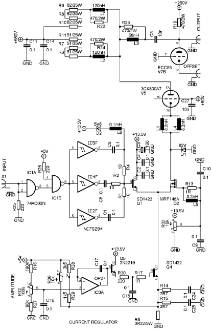
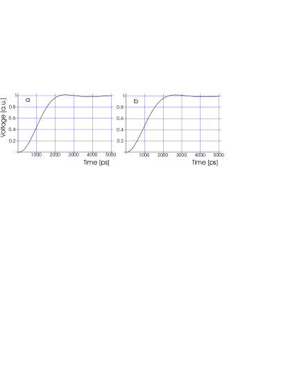
Q1 and Q2 form a differential amplifier. Q1 is biased via D2 and L6, that provide about 5.3V at the base. Between pulses, Q1 conducts and Q2 is cut off. During a pulse, the current is directed through Q2 and the output tube. As it is regulated by Q4 and IC3A, the output amplitude is precisely constant, without feedback over the output stage. Also, the total current being constant, the inductance of the ground connection is not critical. This helps to obtain a very good, fast-rise square-shaped output waveform. Q1 can be a low voltage type, which typically leads to high transition frequency. Since the capacities of Q1 and Q4 are not as critical, transistors capable of high power dissipation can be chosen. The speed of this driver stage is mainly limited by the output capacity of 35 pF of Q2 (MRF148A), and the tube’s input capacity of 30 pF. Inductors L1 and L4 provide series peaking Valley to speed up the signal delivered to the output stage. They are connected to two cathode pins of V5 to control stray inductance. Simulation of this circuit (Fig. 2, a) shows a 10 to 90% rise-time of 1.38 ns.
Q2 is mounted upside down on top of Q1 so that both source leads of Q2 can be connected to Q1 to obtain low parasitic inductance . For example, just 1 nH would contribute about 1.3 ns to the rise-time, where 3 A/5 V is the impedance of this circuit. The Zener diode D1 protects Q2 against excessive voltage. Oscillations at 250 MHz are suppressed by the capacity of D1, the resistors and LR combinations in the base leads of the transistors, and the R-C combinations in the emitter lead of Q4.
The pulser is designed with an output impedance of . Coaxial cables for this are readily available, and the required peak current is reduced to one half of that required for 50 . This impedance together with the load capacity sets a lower limit of about ns for the rise-time. We will closely approach this theoretical limit.
The tube 3CX800A7 Eimacspecs (Eimac division of CPI, Inc.) is chosen primarily for its high gain and can deliver up to 8 A of peak anode current. It requires V drive voltage and 0.2 A peak grid current for 300 V output. A special capacitor (Eimac) having low-inductance, large-area contacts bypasses the grid to ground. The dc grid voltage is adjustable from 20 to about 60 V. The output signal is ac-coupled to the output via C8. V7 is used as a clamp diode to provide a low impedance path for charging C8, thus making the output voltage between pulses very close to zero. Use of a vacuum triode ECC88, connected as a diode, avoids possible pulse distortion associated with the recovery of a semiconductor diode. To minimize stray capacities, it is soldered directly into the circuit without a socket and its internal shield of V7 is left floating. By removing the ground connection at the OFFSET connector, V7 is cut off and a positive bias of 240 V appears at the output. If desired, a potentiometer or a variable voltage between 0 and 10 V at the OFFSET connector can be used to vary the dc level at the output between about 5 and 240 V. This can be used for applying slow, continuous signals to the modulator.
R7-R10 are low-inductance types of very compact design (Ohmite TA025PW82R0JE and TA025PW51R0JE), arranged as depicted in the circuit in a way to minimize stray capacities and inductance. Furthermore, the output circuit consists of L2, L7 (112 nH each) and L3 (56 nH) with paralleled resistors, the output capacity pF of the triode (including circuit strays as measured in our setup), a capacity pF of the diode, and a capacity pF of the resistors. Simulation shows a rise-time of 1.31 ns for the output circuit. The combined risetime of the tube’s driver and output circuits is thus 1.90 ns. Fig. 2 shows the calculated response of the output circuit.
The maximum duty cycle that is permissible for the 3CX800A7 is specified by the ’rms current rule,’ that states that the root mean square (rms) current should not exceed the maximum permissible dc current of 600 mA Eimacspecs . However, when operating the tube as a class B or C radio frequency amplifier, rms currents 1.6-2 times higher are permissible. Using this as the real limit on the rms current, the permissible duty cycle rises by a factor of 2.7-4. Indeed, the data sheets of some tubes specify duty cycles exceeding the rms current rule (e.g., E130L, 8533, 8906). Thus, operation at about 10% duty should be quite safe. With a minimum pulse duration (limited by the rise time) of below 4 ns full width at half maximum, this sets a limit on the repetition rate in excess of 20 MHz.
At 10% duty at =20 MHz and 3.2A peak, the plate of V5 dissipates W including W switching losses assuming 15 pF plate capacity. Q2 dissipates about 26W, including 22W switching losses (assuming that the losses when switching on and off are the same), well within the manufacturer’s specification of 115 W. For Q1 and Q4, losses are 48 W (sum of both transistors) are almost independent of duty cycl between 0 and 10%.
The output amplitude is determined by the setting of the constant-current source by R12. The transistor capacities and circuit impedances change with peak current which may lead to pulse distortion (overshoot and ringing). To prevent this, the dc grid voltage of V5 is adjusted between 20-75 V according to the setting of the constant-current source. The optimum is obtained for such that Q2 is just above saturation.
This leads to a very good square waveform having less than 5%
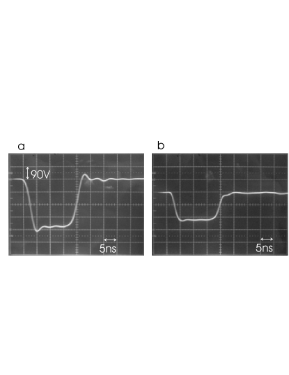
overshoot. At an amplitude 250 V, the rise-time is ns.
This is what is expected from the 1.9 ns theoretical rise-time
for Q2 and the power stage and 1 ns due to the NC7SZ04 inverters
(), but appears too fast in view of
additional influences like Q1’s transition frequency. A possible
reason for that is that provides additional series
peaking. At the maximum amplitude of 340 V, which is limited by
the constant current source, the rise-time increases to 2.7 ns,
see Fig. 3 (a). This may be in part because Q2 is
then operated closer to saturation which increases its capacity
and doesn’t allow its drain potential to swing as required for
series peaking by L1 and L4.
The EOM (New Focus model 4102) uses two lithium niobate crystals
electrically connected in parallel, which receive signals via an
internal 50 strip-line of about 2.5 cm length from an
SMA connector. The total capacity is about 16 pF. Directly
driving this from a cable, ns, even if the pulser output would be
infinitely fast. As this would significantly reduce the overall
speed, we increase match the characteristic impedance of the
strip-line to 93 by reducing its width. As the crystals
are now directly driven from a 93 source, we only need
to consider the crystal capacity of about 12 pF. The speed is
further enhanced by series peaking Valley with an inductor
of 63 nH in series to the crystals. The EOM should now show
ns. With an electrical ns of the pulser,
we expect an optical ns=1.9 ns. The factor of 0.66 is the
theoretical conversion factor for a Gaussian frequency response
and the transfer function of the EOM. This agrees well
with the observed optical ns, Fig. 3 (b).
The circuit can be adapted for analog operation, as a linear amplifier, by driving at the base of Q1. If directly driven from a a generator terminated into , the speed is limited by the capacitive (pF) input impedance of Q1 and the finite transition frequency of Q1, which in connection with the approximately 1.5 Ohmic load due to Q2 appears as an additional effective input capacity of pF (assuming GHz). Thus, the RC time constant is 4.2 ns. With a suitable input network, a rise-time of 6-8 ns should be possible. It can be improved by reducing the impedance, either by a transformer or by an additional emitter follower.
Using a lower value for R5, the maximum output voltage can be increased to 450 V, limited by the maximum collector current of Q1. Using larger transistors is also possible, especially as Q1’s capacity is relatively insignificant. The 3CX800A7 tube enables up to 800 V; if 300 V output or less suffice, a smaller and cheaper tube may be substituted. Using a E130L E130L should lead to similar performance, save for a lower maximum duty cycle.
If the electro-optic crystals and the electronics can be in the same housing, the output impedance can be chosen independently of cable impedances. For a EOM capacity of 12pF plus 6pF tube and wiring capacity, with series-shunt peaking, an electrical rise-time of 3 ns can be achieved with , requiring only 1.5 A peak current. A QQE06/40 tube, that could deliver such current, has an output capacity of 6.4pF.
A previous version of this circuit used a bipolar npn 2N5642 as
Q2. Near the maximum output amplitude of 250 V (lower because of
the voltage rating of the 2N5642), the trailing edge became slow,
about 5-10 ns. Furthermore decreasing the grid potential of V5
eventually leads to saturation of the transistor. This increases
the pulse duration by a few ns, as expected because of the
minority carrier charge storage in the transistor. However, we
accidentally found that it also leads to a speed-up of the
trailing edge. We attribute this to the step recovery effect of
the transistor Paul ; Gerding : As soon as the stored minority
carriers are removed, the transistor switches off rapidly. Thus,
rise and fall times of 3.3 and 3.1 ns were achieved. All 5 tested
samples of 2N5642 (made by Advanced Semiconductor) worked
satisfactorily.
This material is based upon work supported by the National Science Foundation under Grant No. 0400866, the Air Force Office of Scientific Research, and the Multi-University Research Initiative.
References
- (1) E. Stephen Fulkerson, Douglas C. Norman, and Rex Booth in: Digest of Technical Papers. 11th IEEE International Pulsed Power Conference, 1997.
- (2) W.M. Henebry, Rev. Scientific Instrum. 32, 1198 (1961).
- (3) L. Jinyuan, S. Bing, and C. Zenghu, Rev. Sci. Instrum. 69, 3066 (1998).
- (4) T.P. Rutten, N. Wild, and P.J. Veitch, Rev. Sci. Instr. 78, 073108 (2007).
- (5) H. Müller, Rev. Scientific Instrum. 76, 084701 (2005).
- (6) R.M. Walker and H. Wallman in: G.E. Valley and H. Wallman (Eds.), Vacuum-Tube Amplifiers (McGraw-Hill, New York, 1948).
- (7) 3CX800A7 data sheet (Eimac division of CPI, Inc, San Carlos, CA 1987).
- (8) E130L special quality high slope power pentode data sheet (Philips, Eindhoven, 1961) (see, e.g., http://frank.pocnet.net/index.html.).
- (9) R. Paul, Transistoren (Vieweg, Braunschweig, 1965).
- (10) M. Gerding, T. Musch, and B. Schiek, Advances in Radio Science 2, 7-12 (2004).