SmB6: Topological insulator or semiconductor with
valence-fluctuation induced hopping transport?
Abstract
We advert to the fact that presence of valence fluctuations (VFs) in semiconductors with in-gap impurity bands unconditionally leads to dynamical changes (fluctuations) of energies of localized impurity states. We provide arguments that in the impurity subnetwork consisting of centers having energy levels fluctuating around the Fermi energy there exist favorable conditions for hops from occupied states to empty states of less energy. Consequently, we propose original valence-fluctuation induced hopping mechanism as a new possibility to explain unusual metallic-like conduction of SmB6 and other Kondo insulators experimentally observed at lowest temperatures. Interestingly, the proposed mechanism infers enhanced metallic-like surface conductivity of SmB6, what resembles a characteristic property of topological insulator, and is in agreement with experimental observations attempting to prove the existence of topologically protected surface state in SmB6.
SmB6 belongs to the class of materials known as heavy-fermion semiconductors, or alternatively as Kondo insulators Riseborough00 . These materials are characterized by electronic properties, which at high temperatures are associated with a set of independent localized () magnetic moments interacting with a sea of conduction electrons, while at low temperatures their electronic properties resemble those of narrow gap semiconductors Riseborough00 ; Wachter93 ; Antonov2002 . Specifically for SmB6, a small electronic gap ( K) was detected by many experimental techniques, e.g. optical conductivity Travaglini84 , infrared absorption Namba1993 ; Ohta1991 , inelastic neutron scattering Alekseev1993 , electron tunneling Frankowski1982 ; Batkova2008 ; Batkova2006 , and electrical transport measurements Batkova2006 ; Nickerson1971 ; Allen79 ; Batko93 ; Cooley95 ; Flachbart01pb ; Gabani01 .
A fundamental phenomenon that governs physical properties of SmB6 is intermediate valence (or homogeneously mixed valence) of Sm ions that fluctuate between Sm2+ () and Sm3+ () configurations Wachter93 . The Sm2+ : Sm3+ ratio at room temperature is about 4 : 6 and varies with temperature weakly, as established by measurements of lattice constant Tarascon1980 , x-ray absorption Tarascon1980 , and Mössbauer studies Cohen1970 . Studies of spin and charge fluctuations due to Sm2+ Sm fluctuations indicate fluctuation rates in the range of phonon frequencies; the spin fluctuation time obtained via 10B and 11B NMR between 2 and 300 K yields a spin fluctuation rate s-1 Pena1981 , while phonon spectroscopy studies indicate charge fluctuations between 200 cm-1 and 650 cm-1 Zirngiebl86 ; Mock86 , what corresponds to the characteristic charge fluctuation rate, , between s-1 and s-1.
Although SmB6 and other Kondo insulators have been intensively studied for more than four decades, many fundamental aspects of the microscopic description of the mixed valence ground state and the nature of the VFs are still under discussion Antonov2002 . One of the principal questions is whether Kondo insulating materials actually are true insulators at low temperatures or whether small conduction-electron carrier concentration is present Antonov2002 ; Fisk1996 . Answering this question is especially complicated in the case of SmB6 due to a fundamental problem to interpret consistently the electrical resistivity/conductivity behavior at lowest temperatures.
Electrical resistivity measurements of SmB6 show a large resistivity increase at decreasing temperature below 50 K, and saturation at very high residual value at lowest temperatures Allen79 ; Batko93 ; Cooley95 ; Flachbart01pb ; Gabani01 . The corresponding electrical conductivity in the ”saturation region” is metallic-like and reveals a temperature non-activated (metallic) channel in , which becomes dominating below about 3 K Batko93 ; Cooley95 ; Flachbart01pb ; Gabani01 ; Gabani03 . This residual conductivity can be attributed to in-gap states, which were confirmed by other probes Namba1993 ; Ohta1991 ; Caldwell07 ; Miyazaki2012 . However, detailed simultaneous studies of the resistivity and Hall resistivity performed on highest quality SmB6 samples indicate that very high value of would require a superunitary scattering Allen79 ; Cooley95 with unphysically high concentration of scattering centers (at least 80 per unit cell Cooley95 ). Taking into account the Mott-Ioffe-Regel viewpoint, which claims that the conventional Boltzmann transport theory becomes meaningless when the characteristic mean free path of the itinerant conduction electrons becomes comparable to, or less than the interatomic spacing Ioffe60 ; MottDavis81 ; Edwards98 , the very high value of the residual resistivity in SmB6 cannot be attributed to metallic conductivity mediated by itinerant electrons. Thus, some kind of hopping transport is required to describe the conductivity of SmB6 at lowest temperatures. However, hopping-type conduction within the framework of present theoretical models requires a temperature activated conductivity and an insulating ground state, what is in qualitative disagreement with the above mentioned experimental indications Batko93 ; Cooley95 ; Flachbart01pb ; Gabani01 ; Gabani03 . Hence, the origin of the residual resistivity/conductivity in SmB6 can not be consistently explained considering any known mechanism of electrical conductivity in metals or semiconductors if a homogeneous bulk conduction is considered to be responsible for the observed electrical conductivity. Possible solution of this mystery represents recent proposition that SmB6 is a topological Kondo insulator Dzero2010 ; Dzero2012 ; Lu2013 , so that topologically protected metallic surface states can be responsible for the anomalously high residual resistivity. Although several studies indeed indicate metallic surface transport in SmB6 Kim2012 ; Wolgast2013 ; Kim2013 , the question about nature of the surface states in SmB6 remains open. Moreover, new points of view on the origin of the surface enhanced conductivity in SmB6 were recently presented, e.g. polarity driven surface metalicity in SmB6 Zhu2013 or coexistence of non-trivial 2D surface state and trivial surface layer Chen2013 .
The purpose of this paper is to show that there exists also other possibility to explain mysterious residual resistivity of SmB6 within the concept of hopping transport, if effect of VFs of samarium ions on the energy of in-gap impurity states is taken into consideration. Our explanation is based on the fact that Sm2+ Sm fluctuations of valence are intrinsically associated with fluctuations of charge, magnetic moments and ionic radii of samarium ions. Because all these parameters influence the interaction energy of an impurity center with the surrounding lattice (thus influencing the energy of corresponding localized impurity state) it has to be concluded that fluctuations of the mentioned parameters will unconditionally cause fluctuations of energies of localized impurity states in the impurity band of SmB6. As we show in this paper, just fluctuations of energies of impurity states ”driven” by VFs may give rise to a new type of hopping mechanism, which is energetically more favorable at lowest temperatures than the well-known variable-range hopping (VRH). Hopping probability in this new hopping mechanism is governed by dynamics of valence fluctuations and by a characteristic distance between hopping centers, what in case of increased concentration of hopping centers in the surface layer yields correspondingly increased hop probability in the surface layer. The proposed hopping mechanism can be responsible for metallic-like conduction of SmB6 at lowest temperatures, as follows from the analysis and the discussion presented below.

Let us start with a model case of a classic semiconductor having a simple cubic crystal lattice with the lattice parameter , containing metal ions, , positioned in the centers of the elementary cells. Let’s also suppose that metal ions are in two different valency states, say and , where and ions are randomly distributed over the metal ion positions, while their valences are “static”, i.e. they do not change in time. In addition, let us suppose that (i) the considered semiconductor contains localized donor impurity states that form IB in its forbidden gap, (ii) the Fermi energy, , lies in the IB, and (iii) the IB in the vicinity of the Fermi energy is characterized by a constant density-of-states (DOS) function, . The supposed situation is similar to that well-known for doped (classic) semiconductors as schematically depicted in Fig. 1 (see e.g. MottDavis81 ; Shklovskij84 ). So, it is reasonable to suppose that electrical conduction in such system is temperature activated at low temperatures and can be adequately described by hopping process utilizing the concept of Miller-Abrahams network Miller1960 , where randomly distributed impurities form a resistance network, having the nearest neighboring impurities at a typical distance MottDavis81 ; Shklovskij84 ; Mott1968 . However, as noted for the first time by Mott Mott1968 , the activation energy needed to hop should in principle drop to zero at lowest temperatures, from the following reasons. If the electron hops a much bigger distance (say with ) it has a choice of as many sites and may expect to find some with an energy nearer to its own, say with energy difference Mott1968 , where is activation energy defined by Miller and Abrahams Miller1960 as the average energy needed to hop to nearest neighboring impurities at distance . Hopping probability for hops to distance may be written as proportional to Mott1968
| (1) |
where is a localization length. Expression (1) has a maximum when Mott1968
| (2) |
As concluded by Mott, if (2) gives a value of greater than unity, the hopping probability is no longer proportional to but obeys the proportionality
| (3) |
where Mott1968 , and is corresponding hopping probability. Thus, according to the original Mott’s analysis and other more detailed works Mott1968 ; MottDavis81 ; Ambegaokar71 ; Shklovskij84 , conductivity due to electron hops of our model system containing and ions can be written as proportional to at lowest temperatures, while a typical activation energy of a hop, , decreases with temperature as . It can be said that conduction arises from the phonon assisted hopping with a typical activation energy in a so-called optimal band, where the optimal band is defined as a narrow energy interval of the width centered at the Fermi level (see Fig. 1a) with concentration of impurities Shklovskij84
| (4) |
Because concentration of impurities in the optimal band decreases with temperature and approaches zero for [], a typical hop distance () goes to infinity for , resulting in insulating ground state.
Now, let us “turn on” a hypothetical rearrangement process (RP) in the considered semiconductor that causes repetitious changes in distribution of and ions on metal ion positions with a characteristic time constant, . We consider only such rearrangements, where the number of and ions is not changed (i.e. RP is realized via position interchanges of some and ions) and the macroscopic physical properties of the system remain unchanged. (The situation is depicted in Fig. 2.) Due to different physical properties of and ions, changes in space distribution of / ions surrounding an impurity will correspondingly change interaction of the impurity with the surrounding lattice. For instance, “replacement” of by (with relatively smaller radius) will decrease local chemical pressure acting on the neighboring impurity center and increase the attractive Coulomb interaction between the (donor) impurity center and the metal ion. Therefore, RP-caused different redistributions of / ions surrounding an impurity center will result in different energy of the corresponding localized impurity state, , thus will change with a characteristic time constant of the RP, as schematically shown in Fig. 2a.

Performing all possible rearrangements as defined above (i.e. all possible distributions of / ions that do not change macroscopic/bulk physical properties of the material), the energy will change within the interval expressed by the inequality
| (5) |
Here, and () are the minimum and maximum possible energy of the donor, respectively. So that, as follows from the arguments above, the energy of localized impurity/donor state changes with every rearrangement, and lies in energy interval of non-zero width
| (6) |
In other words, the localized impurity/donor state is not longer characterized by energy constant in time (like in semiconductor with absence of RP as depicted in Fig. 1a), but by energy interval (resembling a narrow band), e.g. like shown in Fig. 2b. Probability of finding the localized impurity/donor state at the energy is characterized by partial-DOS function , which is zero outside the interval defined by inequality (5), but might have rather “complex shape” within this interval. For purposes of this paper is considered to be constant within the interval defined by inequality (5), as depicted in Fig. 2b.
RP-caused changes of energy of localized impurity states in time have principal impact on hopping process. According to our original supposition, lies in the IB which is characterized by a constant DOS, and we consider only such redistributions of / ions that do not change physical characteristics of the system (i.e. DOS of the whole macroscopic system remains unchanged). Thus, there have to exist impurity centers with corresponding energy if localized states satisfying the condition , such that
| (7) |
Assuming for simplicity that impurity states are characterized by an equal/typical width of the energy interval , then energies of impurity centers which due to RP can be less, as well as greater than , satisfy the inequality
| (8) |
The concentration of such centers is
| (9) |
Correspondingly, a typical distance between two nearest centers is
| (10) |
Impurity centers defined by (8) have a unique property; there exists a non-zero probability that some occupied donor levels will shift due to RP from the region below to the region above , and analogously, some empty donor levels from the region above will shift under . Such energy changes represent in fact non-equilibrium excitations (driven by RP) that have to be consequently brought into the equilibrium state, what happens via electron hops of “zero activation energy” from occupied states to empty states of less energy. This in fact, indicates a possibility of new hopping mechanism, which should be realized via temperature non-activated hops (tunneling) that have to dominate at lowest temperatures. Let us analyze the situation in more details.
The intrinsic transition rate for an electron hopping from a site with energy to an empty site with energy in the simplest case, when is small compared to , and is of the order of the Debye energy or smaller, is well approximated by the “quantum-limit” hopping formula Ambegaokar71
| (11) | |||
| (12) |
where is a constant as defined elsewhere Ambegaokar71 and is the distance between the centers and . Bidirectional hopping process between the centers and (), in a classic semiconductor (without RP) unconditionally requires thermal activation, because bidirectional hopping always includes also hops to empty states of higher energy [see (11) and Fig. 1a]. For instance, if the first hop is one to a site of less energy, it does not require thermal activation [as follows from (12)]. However, the following hop in opposite direction has to be one to a state of higher energy (see Fig. 1a), so it requires temperature activation [as follows from (11)]. This implicates that bidirectional hopping process is conditioned by energy (phonon) absorption. [In fact, substitution of and in (11) by typical hop distance and activation energy , respectively, yields the same exponential term as (1), which in accordance with Mott’s original deviation Mott1968 (as summarized in the beginning) leads to VRH-conductivity proportional to .]
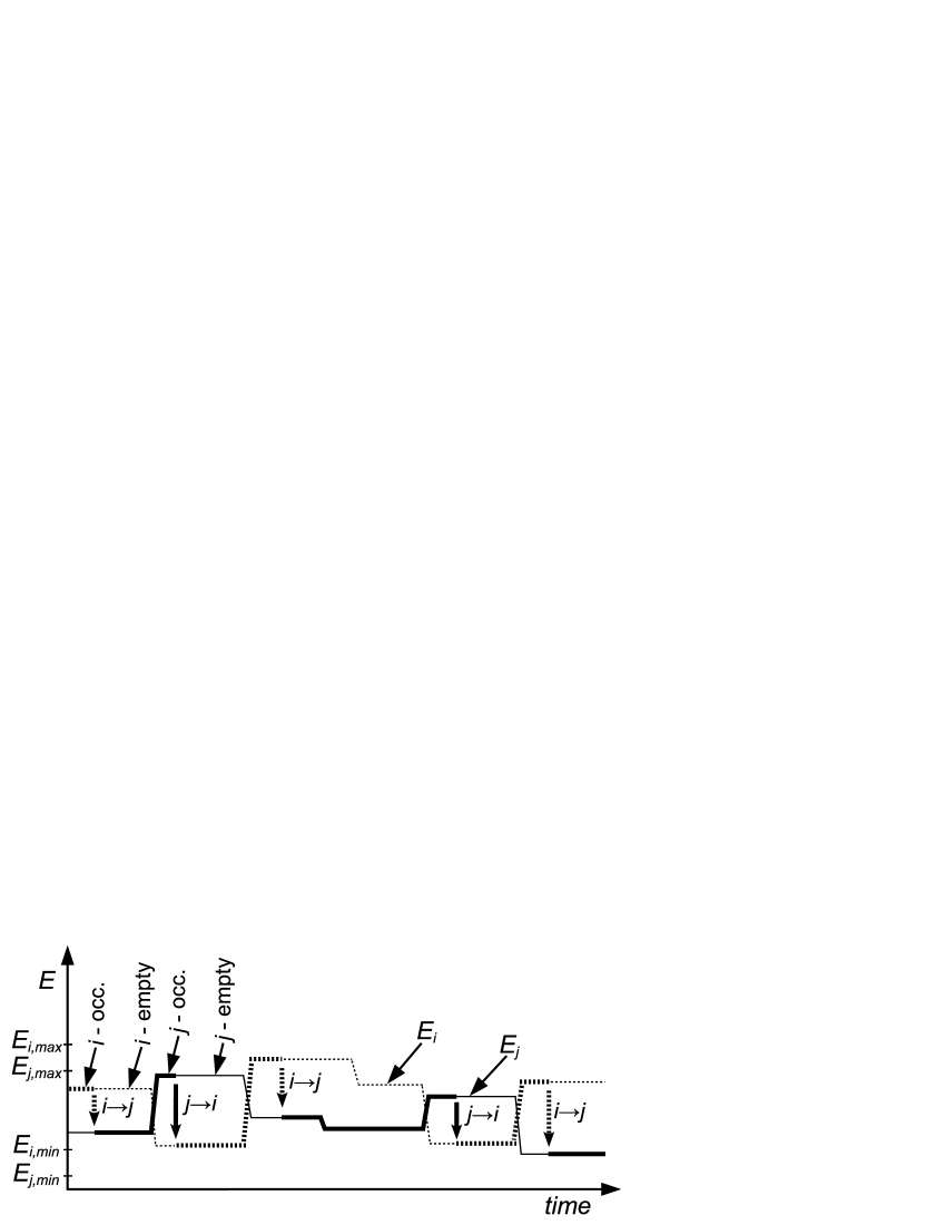
The situation is qualitatively different in a semiconductor, where RP of metal ions takes place, thus energies of impurity states change in time. Let’s consider two impurity states (, ) that have non-zero overlap of their energy intervals (say like shown in Fig. 3), and RP causing repetitive changes of mutual positions of energy levels and . If the first hop (say ) is from an impurity site of (temporarily) higher energy to one of less energy (i.e. ) then it does not require thermal activation (see Fig. 3). However, there exist two possibilities for the hop in the opposite direction (): (i) the hop will require thermal activation if performed during the time period when , or (ii) the hop will be performed without thermal activation after at least one rearrangement of metal ions causing mutual change of relative positions of energy levels and , when becomes (temporarily) greater than , as schematically depicted in Fig. 3. Introducing a parameter () denoting the probability that an occupied state occurs due to RP at (temporarily) higher energy level than an empty state , then the intrinsic transition rate for thermally non-activated electron hop from site to site with (temporarily) less energy will be
| (13) |
while the intrinsic transition rate for thermally activated electron hop from site to site (with temporarily higher energy) will be
| (14) |
If the ratio
| (15) |
is greater than unity, the predominating electron hops between impurity states and are not longer thermally activated, but thermally non-activated hops to states with less energy that are “induced” by RP. Because for every non-zero there exists a temperature providing for , intrinsic transition rate of the considered bidirectional hopping process at lowest temperatures can be in both directions approximated by
| (16) |
However, this practically means that for there is no need for electron to hop to empty state of higher energy, because it is energetically more favorable to ”wait” for a ”proper” rearrangement of ions causing that empty state of less energy occurs (just as it is schematically shown in Fig. 3).
Considering subnetwork of impurities satisfying the inequality (8) we define as the time-averaged probability per unit volume that for a temporarily occupied state belonging to the subnetwork, an empty state from the subnetwork will appear at lower energy as a consequence of RP. Considering electron hops to sites within the distance , where and is given by Eq. (10), electron has choice of as many sites to find an empty state of less energy. Probability of such RP-induced hop, , can be expressed as
| (17) |
and has maximum for . If value , maximum probability of RP-induced hop can be (omitting numerical factors) expressed as
| (18) |
However, estimation of in classic doped semiconductors () Pol-Sklov1991 indicates values . Therefore, predominated hops should be realized to distance (i.e. nearest-neighbor hopping within the considered subnetwork). So, we take to maximize (17), which can be then expressed in the form
| (19) |
Taking into account that both parameters and have finite and non-zero values resulting from RP, and considering that RP is not temperature dependent, it can be concluded that electron hopping induced by RP is temperature non-activated.
The above sketched scenario reveals how RP of metal ions of different valencies in the semiconductor lattice can qualitatively change nature of hopping process. While the hop probability given by proportionality (3) for a system without RP is temperature-activated, presence of RP causes that probability of hops that dominate at lowest temperatures is temperature non-activated. This unique property can be effectively used to explain metallic-like conductivity of SmB6 at lowest temperatures.
Several experimental studies reveal that SmB6 can be adequately treated as a system with IB in the forbidden gap, and with the Fermi energy lying in the IB. Because of nature of VFs, valence fluctuations between Sm2+ and Sm3+ will effect energies of localized impurity states similarly as RP in the model above, i.e., the VFs will cause time-dependent changes (fluctuations) of energy levels of impurity states. (See Fig. 2 and consider SmSm3+ ions instead of ones.) So that, impurity states in SmB6 are expected to be characterized by energy fluctuating in intervals of non-zero width instead of energy levels with energy constant in time. According to the above proposed scenario, and assuming that Fermi energy lies in the impurity band of SmB6, then there will exist impurity subnetwork consisting of impurity centers satisfying condition (8). Hence, mutual position of energies corresponding states in comparison with is dynamically changing (fluctuating), while characteristic rate of these changes is closely related to a characteristic rate VFs. This implicates favorable conditions for hops to empty states of less energy at high hopping rates, which can, in principle, approach rates of VFs. So, based on (19), which we consider as a relevant case to discuss bulk properties of SmB6 [(SmB6)], we can write probability of hops induced by VFs in the considered subnetwork, , as
| (20) |
Here is defined analogously as , accepting the fact that VFs, in principle, represent a special case of RP. Because both parameters and are governed by dynamical processes having origin in VFs (e.g. charge or spin fluctuations), temperature dependence of the probability of VFs-induced hops can be introduced only via effect of temperature on these processes. However, if we take into account generally accepted fact that ground state of SmB6 is valence fluctuating state Riseborough00 ; Wachter93 ; Antonov2002 , then we have to conclude that parameters describing dynamics of VFs (e.g. charge fluctuation rate, ) do not converge to zero for . ¿From this reason, (which is affected by all processes governing fluctuations of impurity energy levels), can not be described by a temperature-activated law, because in such case would have to go to zero for , thus the ground state could not be a valence fluctuating state. Hence, the observed temperature non-activated conduction of SmB6 at lowest temperatures can be reasonably explained by a temperature non-activated nature of dynamics of VFs, which induces temperature non-activated hopping with probability described by (20). ¿From this point of view, observation of almost constant resistivity in SmB6 at lowest temperatures indicates that dynamics of VFs in SmB6 is almost temperature independent for . It can be also said that temperature dependent changes of dynamics of VFs, which consequently influence parameter , should be directly reflected in temperature behavior of electric conduction, as follows from (20). Thus, the proposed scenario not only gives possible explanation for metallic-like resistivity behavior of SmB6, but also gives new physical meaning and interpretation to electrical conductivity data of SmB6 and other valence fluctuating semiconductors at temperatures approaching absolute zero temperature.
Here should be noted that because of the fact that electrical transport is realized via hopping process, corresponding electrical conductivity can be less than the minimum metallic conductivity defined by Mott-Ioffe-Regel criterion. So, the proposed scenario naturally explains why residual conductivity of SmB6 can be less than without need to consider some combination of bulk semiconducting properties (obeying the criterion) and unusual metallic surface state (e.g. topologically protected). Moreover, another surprising consequence of the model proposed here is that it infers existence of enhanced surface conductivity that can be even several orders of magnitude greater than the bulk one, what is in fact, qualitatively the same situation as expected for a Kondo topological insulator state in SmB6.
Relatively higher surface conductivity of SmB6 can be according to the proposed model explained as follows. Direct consequence of (20) is that hopping probability exponentially decreases with increase of hop distance . Typical hop distance in bulk, , can differ from that of the surface, , if bulk and surface concentration of lattice imperfections playing role of hopping centers are different. It is well known that low temperature properties of SmB6 change significantly from sample to sample, indicating important role played by uncontrolled defects, i.e. impurities (typically to in atomic concentrations), small departures from stoichiometry, and structural point defects Nickerson1971 ; Morillo1983 . Experimental results indicate that a typical distance between lattice imperfections in high-quality SmB6 can be several orders of magnitude greater than the lattice parameter, i.e. SmB. However, situation has to be completely different on the surface, because of much greater concentrations of lattice imperfections. The reason is not only “more damaged” surface layer, but also the fact that SmB6 surface is “covered” by unterminated B- and Sm- bonds, which might play role of hopping centers. Considering , or even , and taking into account proportionality (20) it can be reasonably expected that hop probability in the surface layer can reach values in orders of magnitude greater than those in the bulk. Moreover, for completeness of the discussion it should be mentioned that because of relatively less values of and not excluded existence of localized surface states with a localization length, , greater than one in bulk, it may arise situation that parameter will satisfy the condition . In such hypothetical case the value will maximize (17), so that VFs-induced hop probability on the surface will be not expressed by (20), but will be proportional to
| (21) |
what however, indicates a different electrical transport regime. Nevertheless, no matter whether hopping probability in the surface layer of SmB6 is described by (20) or (21) (or even by combination of both of them because of presence of several types of localized surface states) it can be qualitatively concluded that hop probability in the surface layer is relatively greater than in bulk and it is temperature non-activated, i.e. metallic-like. Thus, the proposed scenario is qualitatively consistent with experimental studies of surface transport in SmB6 Kim2012 ; Wolgast2013 ; Kim2013 which have demonstrated metallic surface and insulating bulk separation, as well as studies of SmB6 thin-films, which show systematic decrease of the resistivity and of the ratio with decreasing thin-film thickness Batko1990 . It should be also emphasized that high surface conductivity of SmB6 can be, in principle, a result of combination of several types of conduction mechanisms in surface layer Chen2013 , and here proposed VFs-induced hopping mechanism can be only one of them.
Similar scenario of temperature non-activated hopping type conduction as we propose for SmB6 is expected to be present also in other semiconducting valence-fluctuating systems with IB(s) and Fermi energy lying in the IB. For instance, qualitatively similar resistivity behavior to one of SmB6 was observed also in FeSi Hunt94 ; Paschen97 ; Degiorgi95 and YbB12 Wachter93 ; Batkova2006 . In fact, resistivity/conductivity saturation at lowest temperatures should be a native property (a “fingerprint”) of many “real” VF semiconductors, because impurity states (lattice imperfections) are as a rule introduced during the preparation process of these materials.
In summary, we have provided arguments that presence of valence fluctuations in semiconducting systems having localized in-gap states (impurity band) introduced via lattice imperfections causes corresponding fluctuation of the energy of these states. Consequently, if the Fermi energy lies in the impurity band, energies of in-gap states laying in a certain vicinity of the Fermi energy fluctuate above and below Fermi energy, what creates favorable conditions for hops to empty states of less energy, i.e. without need of activation energy. This give rise to temperature non-activated hopping process with the hop probability governed by dynamics of VFs and concentration of hopping centers. The proposed mechanism is in excellent qualitative agreement with many experimental observations indicating close relationship between concentration of lattice imperfections and residual metallic-like conductivity of SmB6 at lowest temperatures, thus brings possible explanation of unusual metallic like transport in SmB6 (and related Kondo insulators). Moreover, because of the fact that (significantly) increased concentration of lattice imperfections that may play role of hopping centers is expected in the surface layer, it predicts strong enhancement of surface conductivity in SmB6. In this sense the proposed scenario, which utilizes the well established concept of hopping conduction in solids, enables to explain bulk and surface metallic-like properties of SmB6 within common mechanism for bulk and surface conduction, i.e. without need to consider ”unusual” metallic surface conduction, like existence of topologically protected surface. Nevertheless, question about quantitative conductivity estimation in SmB6 (both bulk and surface) due to VFs-induced hopping process and a possible interplay of distinct types of surface conduction in SmB6 remains open and requires further studies.
This work was supported by the Slovak Scientific Agency VEGA (Grant No. VEGA 2-0184-13).
References
- (1) P. S. Riseborough, Advances in Physics 49, 257 (2000).
- (2) P. Wachter, in Intermediate Valence and Heavy Fermions, (Handbook on the Physics and Chemistry of Rare Earths, vol.19, North Holland, 1993).
- (3) V. N. Antonov, B. N. Harmon, and A. N. Yaresko, Phys. Rev. B 66, 165209 (2002).
- (4) T. Travaglini and P. Wachter, Phys. Rev. B 29, 893 (1984).
- (5) T. Namba, H. Ohta, M. Motokawa, S. Kimura, S. Kunii, and T. Kasuya, Physica B 186-188 440 (1993).
- (6) H. Ohta, R. Tanaka, M. Motokawa, S. Kunii, and T. Kasuya, J. Phys. Soc. Jpn. 50 1361 (1991).
- (7) P. A. Alekseev, V. N. Lazukov, R. Osborn, B. D. Rainford, I. P. Sadikov, E. S. Konovalova, Yu. B. Paderno, Europhys. Lett. 23, 347 (1993).
- (8) L. Frankowski and P. Wachter, Solid State Commun. 41, 577 (1982).
- (9) M. Batkova, I. Batko, E. S. Konovalova, N. Shitsevalova, Y. Paderno, Acta Phys. Pol. A 113 255 (2008).
- (10) M. Batkova, I. Batko, E. S. Konovalova, N. Shitsevalova, Y. Paderno, Physica B 378-380 618 (2006).
- (11) J. C. Nickerson, R. M. White, K. N. Lee, R. Bachmann, T. H. Geballe, and G. W. Hull Jr., Phys. Rev. B 3, 2030 (1971).
- (12) J. W. Allen, B. Batlogg, and P. Wachter, Phys. Rev. B 20, 4807 (1979).
- (13) I. Bat’ko, P. Farkašovský, K. Flachbart, E. S. Konovalova, and Yu. B. Paderno, Solid State Commun. 88, 405 (1993).
- (14) J. C. Cooley, M. C. Aronson, Z. Fisk, and P. C. Canfield, Phys. Rev. Lett. 74, 1629 (1995).
- (15) K. Flachbart, S. Gabáni, E. Konovalova, Y. Paderno, and V. Pavlík, Physica B 293, 417 (2001).
- (16) S. Gabáni, K. Flachbart, E. Konovalova, M. Orendáč, Y. Paderno, V. Pavlík, and J. Šebek, Solid State Commun. 117, 641 (2001).
- (17) S. Gabáni, E. Bauer, S. Berger, K. Flachbart, Y. Paderno, C. Paul, V. Pavlík, and N. Shitsevalova, Phys. Rev. B 67, 172406 (2003).
- (18) J. M. Tarascon, Y. Isikawa, B. Chevaliere, J. Etorneau, P. Hagenmuller, and M. Kasaya, J. de Phys. 41, 1141 (1980).
- (19) R. L. Cohen, M. Eibschutz, K. W. West, and E. Buller, J. Appl. Phys. 41, 898 (1970).
- (20) O. Peña, D. E. MacLaughlin, M. Lysak, and Z. Fisk, J. Appl. Phys. 52, 2152 (1981).
- (21) E. Zirngiebl, S. Blumenroder, R. Mock, and G. Güntherodt, JMMM 54-57, 359 (1986).
- (22) R. Mock, E. Zirngiebl, B. Hillebrands, G. Güntherodt, and F. Holtzberg, Phys. Rev. Lett. 57, 1040 (1986).
- (23) Z. Fisk, J. L. Sarrao, S. L. Cooper, P. Nyhus, G. S. Boehinger, A. Passner, and P. C. Canfield, Physica B 223-224 409 (1996).
- (24) T. Caldwell, A. P. Reyes, W. G. Moulton, P. H. Kuhns, M. J. R. Hoch, P. Schlottmann, and Z. Fisk, Phys. Rev. B 75, 075106 (2007).
- (25) H. Miyazaki, T. Hajiri, T. Ito, S. Kunii, and S. Kimura, Phys. Rev. B 86, 075105 (2012).
- (26) P. P. Edwards, R. L. Johnston, C. N. R. Rao, D. P. Tunstall, and F. Hensel, Phil. Trans. R. Soc. Lond. A 356, 5 (1998).
- (27) A. F. Ioffe and A. R. Regel, Prog. Semicond. 4, 237 (1960).
- (28) N. F. Mott and E. Davis in Electronic Processes in Non-Crystalline Materials (Calendron Press, Oxford, 1971).
- (29) M. Dzero, M. Sun, K. Galitski, and P. Coleman, Phys. Rev. Lett. 104, 106408 (2010).
- (30) M. Dzero, M. Sun, P. Coleman , and K. Galitski, Phys. Rev. B 85, 045130 (2012).
- (31) F. Lu, J.Z. Zhao, H. Weng, and Xi. Dai, Phys. Rev. Lett. 110, 096401 (2013).
- (32) D. J. Kim, T. Grant, and Z. Fisk, Phys. Rev. Lett. 109, 096601 (2012).
- (33) S. Wolgast, C. Kurdak, K. Sun, J. W. Allen, Dae-Jeong Kim, and Z. Fisk, Phys. Rev. B 88, 180405(R) (2013).
- (34) D. J. Kim, S. Thomas, T. Grant, J. Boltimer, Z. Fisk and JingXia, Sci. Rep. 3, 3150 (2013).
- (35) Z.-H. Zhu, Phys. Rev. Lett. 111, 216402 (2013).
- (36) F. Chen, C. Shang, A. F. Wang, X. G. Luo, T. Wu, and X. H. Chen, arXiv:1309.2378v2.
- (37) N. F. Mott, J. Non-Cryst. Solids, 1, 1 (1968).
- (38) B. I. Shklovskii and A. L. Efros in Electronic Properties of Doped Semiconductors, (Springer Series in Solid State Sciences, 1984).
- (39) A. Miller, and E. Abrahams, Phys. Rev. B 4, 2612 (1971).
- (40) V. Ambegaokar, B. I. Halperin, and J. S. Langer, Phys. Rev. 120, 745 (1960).
- (41) J. Morillo, C.H. de Novion, Solid State Commun. 48, 315 (1983).
- (42) See A.R. Long in Hopping Transport in Solids, Modern Problems in Condensed Matter Sciences, 28, 207-231 (1991), and references therein.
- (43) M. B. Hunt, M. A. Chernikov, E. Felder, H. R. Ott, Z. Fisk, and P. Canfield, Phys. Rev. B 50, 14933 (1994).
- (44) S. Paschen, E. Felder, M. A. Chernikov, L. Degiorgi, H. Schwer, H. R. Ott, D. P. Young, J. L. Sarrao, and Z. Fisk, Phys. Rev. B 56, 12916 (1997).
- (45) L. Degiorgi, M. Hunt, H. R. Ott, and Z. Fisk, Physica B 206-207, 810 (1995).
- (46) I. Batko, K. Flachbart, J. Miškuf, V. M. Filipov, E. S. Konovalova, Ju. B. Paderno, J. Less-Common Met. 158 L17 (1990).