Development of an n-channel CCD, CCD-NeXT1, for Soft X-ray Imager onboard the NeXT satellite
Abstract
NeXT (New X-ray Telescope) is the next Japanese X-ray astronomical satellite mission after the Suzaku satellite. NeXT aims to perform wide band imaging spectroscopy. Due to the successful development of a multilayer coated mirror, called a supermirror, NeXT can focus X-rays in the energy range from 0.1 keV up to 80 keV. To cover this wide energy range, we are in the process of developing a hybrid X-ray camera, Wideband X-ray Imager (WXI) as a focal plane detector of the supermirror. The WXI consists of X-ray CCDs (SXI) and CdTe pixelized detectors (HXI), which cover the lower and higher X-ray energy bands of 0.1–80 keV, respectively. The X-ray CCDs of the SXI are stacked above the CdTe pixelized detectors of the HXI. The X-ray CCDs of the SXI detect soft X-rays below keV and allow hard X-rays pass into the CdTe detectors of the HXI without loss. Thus, we have been developing a “back-supportless CCD” with a thick depletion layer, a thinned silicon wafer, and a back-supportless structure. In this paper, we report the development and performances of an evaluation model of CCD for the SXI, “CCD-NeXT1”. We successfully fabricated two types of CCD-NeXT1, unthinned CCDs with 625-m thick wafer and 150- thick thinned CCDs. By omitting the polishing process when making the thinned CCDs, we confirmed that the polishing process does not impact the X-ray performance. In addition, we did not find significant differences in the X-ray performance between the two types of CCDs. The energy resolution and readout noise are eV (FWHM) at 5.9 keV and electrons (RMS), respectively. The estimated thickness of the depletion layer is . The performances almost satisfy the requirements of the baseline plan of the SXI.
keywords:
NeXT satellite; Soft X-ray Imager; X-ray CCD; back-supportless CCD; CCD-NeXT1PACS:
95.55.-n, 95.55.Aq, 95.55.Ka,, , , , , , , , , , ,
1 Introduction
NeXT (New X-ray Telescope) is the sixth Japanese X-ray astronomical satellite mission, which is proposed to be launched around 2012. A Hard X-ray Telescope (HXT), supermirror onboard NeXT (see Tawara et al. (2003) [1] and references therein), has a large collecting area for X-rays in the energy from 0.1 to 80 keV. In particular, the HXT has a high reflectivity even in the hard X-ray band above 10 keV. Previous satellite missions have not had X-ray focusing optics capable of observations in this band. NeXT is designed to be the first to perform imaging and spectroscopic observations in the energy band above 10 keV. In order to meet the energy range covered by the HXT, we have been developing a Wideband X-ray Imager (WXI).
The first successful space flight use of X-ray CCDs as photon counting and spectroscopic imagers was the SIS aboard [2]. Since then, X-ray CCDs have become standard focal plane detectors for X-ray telescopes in the X-ray energy band of 0.1–10 keV, and have been adopted as the principal detectors of recent X-ray observatories such as the ACIS of Chandra [3], the EPIC of XMM-Newton [4, 5], and the XIS of Suzaku [6] because X-ray CCDs have well balanced spectroscopic, imaging, and time resolution performances. However, to achieve a quantum efficiency of 10% for X-rays with an energy of 40 keV, a depletion layer is required, which is nearly impossible. A detector with a high-Z material is essential for observations in the hard X-ray band above 10–20 keV. On the other hand, the performances of imaging and spectroscopy below 10 keV of high-Z solid detectors such as CdTe detectors are poorer than those of X-ray CCDs, suggesting that a single detector cannot cover the entire 0.1–80 keV band with the best X-ray performance. Thus, we have been developing a hybrid camera, the Wide band X-ray Imager (WXI), which combines an X-ray CCD and a CdTe pixelized detector [7, 8, 9, 10]. Holland (2003) [11] has also reported the first laboratory demonstration of such a hybrid detector with a thinned X-ray CCD, which is operated in front of CZT detector.
The WXI consists of two sub-instruments; the Soft X-ray Imager (SXI) and the Hard X-ray Imager (HXI); overviews can be found in Tsuru et al. (2005) [12] and Takahashi et al. (2004) [13], respectively. The SXI and HXI are the upper and lower parts of the WXI, respectively. The SXI consists of X-ray CCDs with a thick depletion layer for the lower energy band below 10–20 keV. The HXI is based on CdTe pixelized detectors, which cover the hard X-rays above 10–20 keV.
We have developed a new type of CCD for the SXI, a “Back-Supportless CCD” (BS-CCD), in which the back supporting package under the imaging area of the CCD is removed. Most X-rays absorbed in the field-free region of the CCD are undetected and lost. Hence, we also removed the field-free region as much as possible. The BS-CCD of the SXI is placed over the CdTe pixelized detectors of the HXI. Soft X-rays are detected in the BS-CCD, while hard X-rays penetrate through the BS-CCD and are detected by the CdTe pixelized detectors. Thus, both soft and hard X-rays are detected without loss.
As previously reported by Tsuru et al. (2005) [12] in detail, we have been developing a BS-CCD for the SXI following two plans of a rather conservative “baseline plan” and an innovative “goal plan” in parallel. Table LABEL:tab:SXIgoala shows the specifications of the BS-CCD of the two plans along with those of the XIS [6], which is one of the most excellent X-ray CCDs currently in orbit.
In the goal plan, we realize a fully-depleted back-illuminated type of BS-CCD with a very thick depletion layer of by adopting a p-channel device. We have already successfully fabricated test devices with a full depletion layer, which was 200- thick. The details and status of the developments are reported elsewhere [14, 15, 16, 17, 18, 19].
In the baseline plan, we developed BS-CCDs based on a natural extension of our successful developments of CCD-CREST/CREST2 and MAXI-CCD in order to minimize the risk involved with their development [20, 21, 22, 23]. We adopted a front-illuminated type of CCD mainly due to the manufacturing process [15]. The thickness of the depletion layer is designed to be 70–80 or more. We have already successfully developed a small test model of BS-CCD and confirmed that the thinning processes of the wafer and the back-supportless structure do not degrade the performance [15]. After the successfully developing the small test model, we constructed an evaluation model, “CCD-NeXT1”. Following CCD-NeXT1, we will develop a flight model, “CCD-NeXT2”, which matches the specifications of the SXI shown in Table 1. In this paper, we report the development and the performance of CCD-NeXT1111Note that part of the results reported herein have already been reported as a contributing paper of a SPIE conference [24]..
2 Specification of CCD-NeXT1
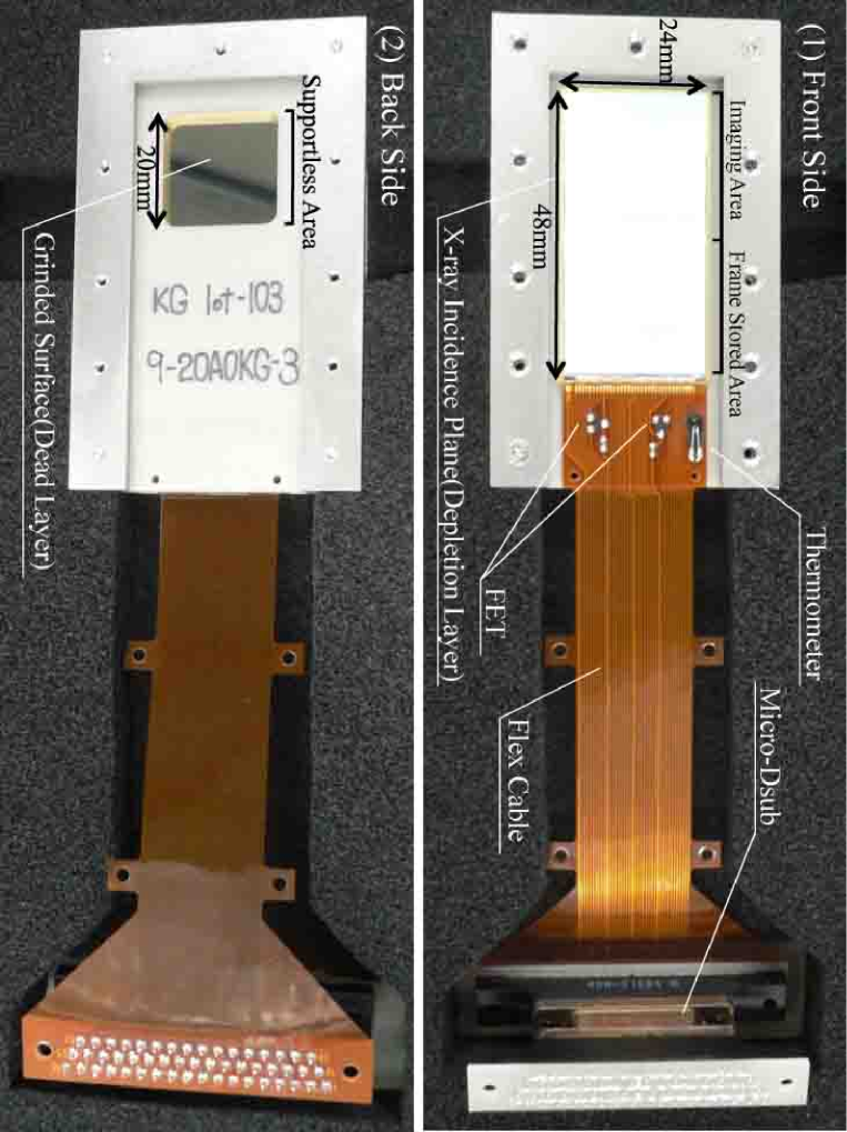
Table 2 shows the specifications of CCD-NeXT1. CCD-NeXT1 is a frame transfer type of CCD with an imaging area (IA) and a frame-stored area (FS). The format and pixel size are pixels and both in the IA and FS, respectively. The size of IA is . CCD-NeXT1 has two readout nodes.
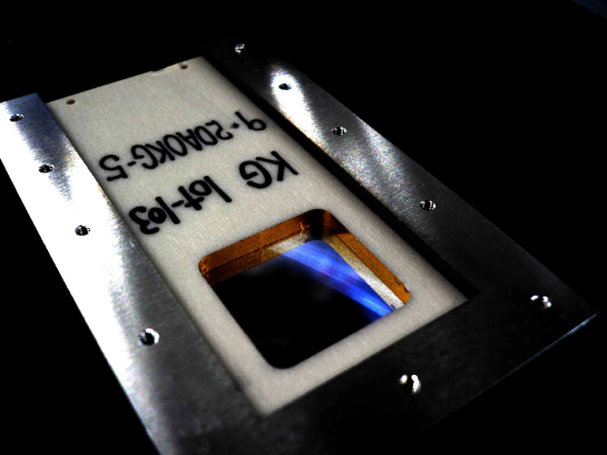
Figure 1 shows pictures of the CCD-NeXT1 device. The front and back sides of the package are open and the surfaces of both sides of the device can be seen. Because the surface of the CCD-NeXT1 device is coated with evaporated aluminum for optical blocking, the reflections on the surface of both sides are observed in Figure 1.
First, we tested the unthinned type of CCD-NeXT1 with 625- thick silicon wafers to determine if the CCDs were successfully processed. Next, we fabricated CCD-NeXT1 devices processed on 150- thinned wafers and test them. Both devices were fabricated on wafers with a high specific resistance of .
3 Performances of CCD-NeXT1
3.1 Unthinned device
We uniformly irradiated the IA of the unthinned CCD-NeXT1 device with 55Fe and 109Cd X-rays. The FS was covered by a thick aluminum plate to block incident X-rays. The CCD-NeXT1 device was driven in a frame transfer mode and the signal was read out through both of the nodes (hereafter referred to as nodes A and B). We performed the clocking and readout of the device with the MiKE CCD operation system, which was developed at Osaka University [23]. Table 3 summarizes the results, while Figure 2 shows the acquired spectra from the 55Fe and 109Cd sources, where single pixel events and multi-pixel events within pixels ( grade 0–7 [25]) were accumulated for 55Fe and 109Cd, respectively. The energy resolutions of nodes A and B for 5.9 keV X-rays were and , respectively. We fitted a single Gaussian function to the histograms of the horizontal over clock regions and obtained readout noises of and for nodes A and B, respectively. The node sensitivity of this device was , which is higher than that of the test model of BS-CCD [15]. The readout noise of CCD-NeXT1 was also the same as that of the test model of BS-CCD [15]. Both vertical and horizontal CTIs are as good as those of the test model of BS-CCD [15] and satisfy the requirements for the baseline plan of SXI.
We measured the detection efficiency and estimated the thickness of the depletion layer using X-rays from 109Cd. We collimated the X-rays to expose only the IA of the CCD-NeXT1 device. The absolute X-ray flux of the source was well-calibrated. In this experiment, the sum of the absolute flux of and was calibrated, but the individual contributions were not separately calibrated. The detection rate of was , which corresponds to a detection efficiency of % and is consistent with an 84- thick depletion layer.
3.2 Thinned device
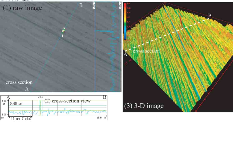
To thin the wafers of the tested model of BS-CCD, we adopted a combination of grinding and polishing methods [15]. We found that the polishing process often physically destroy the CCD wafers, which impacts the yield of the CCD-NeXT1 devices. Thus, we processed devices with a wafer thickness of by omitting the polishing process in order to examine their feasibility as X-ray detectors. We examined the surfaces of the devices with a color laser three-dimensional profiling microscope (VK-9500; Keyence) and found that numerous microscopic striations were left on the surface due to the omission of the polishing process. Figure 3 is a close-up view of the ground surface of the CCD-NeXT1 device, which shows the striations. Figure 4 shows the condition of the ground surface. We found the depth and width of the striations to be less than peak-to-peak and sub-, respectively. Compared to the wafer thickness () and the size of pixels (), these trails are negligibly small. Therefore, we concluded that grinding only is sufficient for the thinning process.
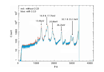
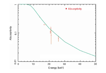
We investigated X-ray performance of the thinned devices fabricated without the polishing process. First, we measured the wafer thickness of the device to confirm it was as designed. We placed the IA (back-supportless area) of the CCD-NeXT1 device between an 241Am source and the CdTe detector (XR-100T-CdTe; AmpTek) to acquire an “absorbed” 241Am spectrum. Subsequently, we detached the CCD-NeXT1 device and acquired an “unabsorbed” spectrum using the same experimental setup. The left panel in Figure 5 shows the two spectra. The intensity ratio of each characteristic X-ray line between the absorbed and unabsorbed spectra shows the X-ray transmission properties () of this wafer. Therefore the absorptivity () was . We measured the at each characteristic X-ray line and found it is consistent with a silicon thickness of (the right panel of Figure 5). Thus, we confirmed that the wafer of the thinned device is 150- thick, as designed.
Second, we investigated the X-ray performance of the thinned device by conducting the same experiments mentioned in the previous section for an unthinned device. Figure 6 shows the acquired spectra of single pixel events from an 55Fe source and ASCA grade 0–7 events from an 109Cd source. The readout noise and the energy resolution were (RMS) and eV (FWHM) at the 5.9 keV (Table 3), respectively. CTIs were both for the vertical and horizontal transfers. It should be noted that the CCD was read out through node A.
Finally, we measured the detection efficiency by the irradiating the CCD with the collimated 109Cd source as previously described. We obtained a detection efficiency for the two lines by comparing the obtained count rate with the absolute flux of the 109Cd X-rays. In this experiment, the absolute fluxes of Ag Kα and Kβ were calibrated separately. The detection efficiencies were 5.5% and 3.5% for the Ag Kα and Kβ, respectively, implying a 76- thick depletion layer.
From the results described above, the X-ray performance of the thinned device was essentially equivalent to that of the unthinned device and the test model of BS-CCD [15]. Hence we concluded that the thinned CCD-NeXT1 device satisfied the requirements for the X-ray performance of the baseline plan for the SXI.
4 Summary
-
•
Following the successful development of the test models of BS-CCD for SXI onboard the NeXT satellite, we developed an evaluation model, CCD-NeXT1. We fabricated two types of CCD-NeXT1. One was a type of un-thinned CCD with 625-m thick wafers. The other type was a thinned CCD with 150- thickness.
-
•
We processed thinned CCD-NeXT1 devices by omitting the polishing process in the thinning process. The evaluation of the devices confirmed that omitting the polishing process did not impact on the X-ray performance.
-
•
We did not observe a significant difference in the X-ray performance of the unthinned and the thinned devices. The energy resolution and the readout noise were 140 eV (FWHM) at 5.9 keV and 5 electrons (RMS), respectively. The detection efficiency of the photons indicates that the depletion layer is 80- thick. This performance meets the requirements for the baseline plan of the SXI.
ACKNOWLEDGMENTS
This work is based upon the Grant-in-Aid for the 21st Century COE “Center for Diversity and Universality in Physics” from the Ministry of Education, Culture, Sports, Science and Technology (MEXT) of Japan, and is supported by a Grant-in-aid (Fiscal Year 2002-2006) for one of the Priority Research Areas in Japan; “New Development in Black Hole Astronomy”. This work is partly supported by a Grant-in-Aid for Scientific Research by the Ministry of Education, Culture, Sports, Science and Technology of Japan (16002004). T.I. is supported by JSPS Research Fellowship for Young Scientists.
References
- [1] Tawara, Y., Kunieda, H., Inoue, H., Mitsuda, K. Ogasaka, Y. and Takahashi, T., Proc. SPIE 4851, (2003), 324
- [2] Byrke, B. E., Mountain, R. W., Harrison, D. C., Bautz, M. W., Doty, J. P., Ricker, G. R., Daniels, P. J. IEEE Trans. ED, 38, (1991) 1069
- [3] Garmire, G. P., Bautz, M. W., Ford, P. G., Nousek, J. A., & Ricker, G. R., Jr.,Proc. SPIE, 4851, (2003), 28
- [4] L. Strüder, et al., Astron. & Astrophys., 365, (2001), L18
- [5] M. Turner et al., Astron. & Astrophys., 365, (2001), L27
- [6] Koyama, K., et al., Publ. Astron. Soc. Jpn., 59, (2007), 23
- [7] Takahashi, T., Paul, B., Hirose, K., Matsumoto, C., Ohno, R., Ozaki, T., Mori, K., Tomita, Y., Nucl. Instrum. & Method A, 436, (1999), 111
- [8] Tsuru, T. G., Bamba, A., Imanishi, K., Kohno, M., Koyama, K., Murakami, H., Tsujimoto, M., Tanimori, T., Ueno, M., Proc. ASP Conference, 251, (2001), 596.
- [9] Tsuru, T. G., Tanimori, T., Bamba, A., Imanishi, K., Koyama, K., Kubo,K., Matsumoto, H., Miuchi, K., Nagayoshi T., Orito, R., Takada, A., Takagi, S., Tsujimoto, M., Ueno, M., Tsunemi, H., Hayashida, K., and Miyata, E., Advances in Space Research, 34, (2004), 2688
- [10] Takahashi, T., Makishima, K., Fukazawa, Y., Kokubun, M., Nakazawa, K., Nomachi, M., Tajima, H., Tashiro, M., and Terada, Y., New Astronomy Review 48, (2004), 269
- [11] Holland, A.D.,Nucl. Instrum. & Method A, 513 (2003) 308.
- [12] Tsuru, T. G., Takagi, S., Matsumoto, H., Inui, T., Koyama, K., Tsunemi, H., Hayashida, K., Miyata, E., Dotani, T., Ozaki, M., Awaki, H., Kitamoto, S., Kohmura, T., Nucl. Instrum. & Method A, 541, (2005), 392
- [13] Takahashi, T., Awaki, H., Dotani, T., Fukazawa, Y., Hayashida, K., Kamae, T., Kataoka, J., Kawai, N., Kitamoto, S., Kohmura, T., Kokubun, M., Koyama, K., Makishima, K., Matsumoto, H., Miyata, E., Murakami, T., Nakazawa, K., Nomachi, M., Ozaki, M., Tajima, H., Tashiro, M., Tamagawa, T., Terada, Y., Tsunemi, H., Tsuru, T., Yamaoka, K., Yonetoku, D., Yoshida, A., Proc. SPIE, 5488, (2004), 549
- [14] Kamata, Y., Miyazaki, S., Tsunemi, M., Miyata, E., Takagi, S., Tsuru, T. G, Miyaguchi, K., and Suzuki, H., Proc. SPIE, 5499, (2004), 210
- [15] Takagi, S., Tsuru, T. G, Matsumoto, H., Koyama, K., Tsunemi, H., Miyata, E., Miyazaki, S., Kamata, Y., Miyaguchi, K., Muramatsu, M., Suzuki, H., Nucl. Instrum. & Method A, 541, (2005), 385
- [16] Kamata, Y., Miyazaki, S., Nakaya, H., Tsuru, T. G, Takagi, S., Tsunemi, H., Miyata, E., Muramatsu, M., Suzuki, H., Miyaguchi, K., Proc. SPIE, 6276, (2006), 52
- [17] Matsuura, D., Tohiguchi, M., Ozawa, H., Miyata, E., Tsunemi, H., Takagi, S., Inui, T., Tsuru, T. G., Kamata, Y., Miyazaki, S., Nakaya, H., Miyaguchi, K., Muramatsu, H., Suzuki, H., Proc. SPIE, 6276, (2006), 33
- [18] Takagi, S., Tsuru, T. G., Inui, T., Ozawa, M., Matsumoto, H., Koyama, K., Tsunemi, H., Miyata, E., Matsuura, D., Tohiguchi, M., Miyazaki, S., Kamata, Y., Miyaguchi, K., Muramatsu, M., Suzuki, H., Proc. SPIE, 6266, (2006), 115
- [19] Tsuru, T. G., Takagi, S.-I., Matsumoto, H., Inui, T., Ozawa, M., Koyama, K., Tsunemi, H., Hayashida, K., Miyata, E., Ozawa, H., Touhiguchi, M., Matsuura, D., Dotani, T., Ozaki, M., Murakami, H., Kohmura, T., Kitamoto, S. and Awaki, H., Proc. SPIE, 6266, (2006), 74
- [20] Bamba, A., Kohno, M., Murakami, H., Imanishi, K., Tsujimoto, M., Tsuru, T. G., Koyama, K., Awaki, H., Kitamoto, S., Hayashida, K., Katayama, H., Tsunemi, T. , Proceedings of New Century of X-ray Astronomy, ASP Conference Series, 251, (2001), 519
- [21] Tsunemi, H., Nucl. Instrum. & Method A, 541, (2005), 295
- [22] Tomida, H., et al., Proc. SPIE, 4012, (2000), 178
- [23] Miyata, E., Natsukari, C., Kamazuka, T., Kouno, H., Tsunemi, H., Matsuoka, M., Hamaguchi, K., Nucl. Instrum. & Method A, 488, (2002), 184
- [24] Ozawa, H., Tohiguchi, M., Matsuura, D. Miyata, E., Tsunemi, H., Takagi, S.-i., Inui, T., Tsuru, T. G., Kamata, Y., Nakaya, H., Miyazaki, S., Miyaguchi, K., Muramatsu, M., Suzuki, H., Proc. SPIE, 6266, (2006), 770
- [25] Yamashita, A., Dotani, T., Ezuka, H., Kawasaki, M., & Takahashi, K., Nucl. Instrum. & Method A, 436, (1999), 68


| Item | Baseline plan | Goal plan | Suzaku XIS |
|---|---|---|---|
| Readout noise | (same) | ||
| Energy resolution† | (same) | 130 eV | |
| Wafer type | N channel | P channel | N channel |
| Imaging area | (same) | ||
| Pixel size♭ | (same) | ||
| Readout nodes | 8 | 8 | 4 |
| Depletion layer | 70–100 | 200 | (FI), (BI) |
| Field-free layer | 50–80 | 0 | (FI), (BI) |
| Illuminated type | front illuminated | back illuminated | both types |
| Surface coating | aluminum | aluminum | none |
| †: Energy resolution for Mn (5.9 keV) X-rays (FWHM). | |||
| ♭: Values in imaging area. | |||
| Number of pixels | 2000 2000 2† |
|---|---|
| Pixel size | 12 m 12 m |
| Clock phase | 2 phase |
| Transfer method | Frame Transfer |
| Readout nodes | 2 |
| Depletion layer | 70–100 |
| wafer thickness | 150 or 625 |
| Illuminated type | front illuminated |
| Surface coating | aluminum |
| † Sum of imaging area and frame stored region. | |
| parameter | unthinned device | thinned device | |
|---|---|---|---|
| readout node | A | B | A |
| Readout noise in rms (e-) | |||
| Energy resolution (eV)† | |||
| Depletion layer () | 84 | 76 | |
| Wafer () | 625 (not thinned) | 150 | |
| Horizontal CTI | |||
| Vertical CTI | |||
| Errors are at | |||
| † Energy resolutions are for Mn (5.9 keV) X-rays (FWHM). | |||