Monolithic Pixels R&D at LBNL
Abstract
This paper reports recent results from the ongoing R&D on monolithic pixels for the ILC Vertex Tracker at LBNL [1].
1 Introduction
A Laboratory Directed Research and Development (LDRD) program has been on-going at LBNL since 2005. The main activity on sensor R&D is the development of CMOS monolithic pixels with integrated functionalities and fast readout in view of their possible application in the ILC Vertex Tracker. At each step of the development, various pixel architectures and layout options are explored, driving the choice for the design of subsequent prototypes.
The results obtained with the first prototype designed at LBNL (the LDRD-1 chip) have been reported in [2]. This paper summarizes the recent results obtained with the second prototype of the LDRD family, the LDRD-2 chip implementing in-pixel Correlated Double Sampling (CDS), outlines the main features of a forthcoming prototype with integrated digitization, and finally introduces a line of research recently started on Silicon-On-Insulator (SOI) pixels.
2 CMOS Monolithic Pixel Sensors
2.1 Prototype with in-pixel CDS and fast readout
The LDRD-2 chip was designed and fabricated in 2006 using the AMS 0.35 m CMOS-OPTO technology with a nominal epilayer thickness of 14 m. The array of 9696 pixels of 20 m pitch is divided in 6 subsections with different sizes of the charge collecting diode (33 m2 and 55 m2) and different pixel architectures, standard 3-transistor (3T) pixels with and without a guard-ring around the diode and a self-biased pixel architecture, similar to the one first proposed in [3].
All sectors implement in-pixel CDS: the pixel dark level and charge signal are consecutively stored on two capacitors integrated in each pixel; both signals are then clocked to the chip analog outputs, after which the CDS difference is obtained either via FPGA or via the online DAS. The chip was designed to be operated up to a clocking frequency of 25 MHz. The readout scheme is based on a rolling-shutter scheme, i.e. rows are reset and read out in sequence, so that the integration time is constant for all pixels.
The LDRD-2 has been extensively tested using the same measurement protocol used for the LDRD-1 chip: in-lab calibrations with a 55Fe source and lasers of different wavelengths have been performed. The sensor charge collection time has been determined using a fast (0.5-5 ns) 1060 nm laser pulse focused on a single pixel and by following the collected charge signal during the pixel sampling time. The result of 150 ns agrees well with the expectations coming from the typical resistivity of the epitaxial layer employed in the fabrication process.
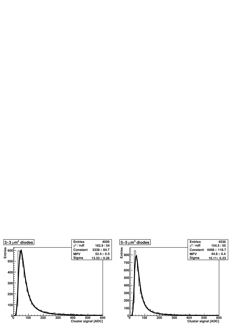
The sensor response to minimum ionising particles has been tested on the 1.5 GeV electron beam at the BTS line of the Advanced Light Source (ALS) at LBNL. Figure 1 shows the cluster signal distribution obtained for the two different diode sizes on the chip sectors featuring a 3T pixel architecture. An average S/N ratio of 20 was found to be similar for the two different diode sizes, with an average cluster multiplicity between 4 and 5, the larger being associated with pixels equipped with smaller diodes. The most probable value for the cluster charge signal for small and big diodes is 750 and 1000 electrons, respectively.
2.2 Prototype with integrated ADCs
The LDRD-3 chip, which is being designed and will be submitted in July in the 0.35 m AMS CMOS-OPTO process, features the same in-pixel CDS architecture as in the LDRD-2 prototype, combined with integrated ADCs at the end of each column. The pedestal and signal levels from each pixel are sent to the bottom of the column, the CDS difference being performed by a 5-bit successive approximation, fully differential ADC running at 300 MHz clock frequency. The design of the LDRD-3 chip is driven by the results of a detailed study performed on data collected with the LDRD-1 chip for different pixel pitches, which had shown that 5-bit ADC accuracy is sufficient to achieve the desired single point resolution, provided that the pixel pedestal can be removed before digitization.
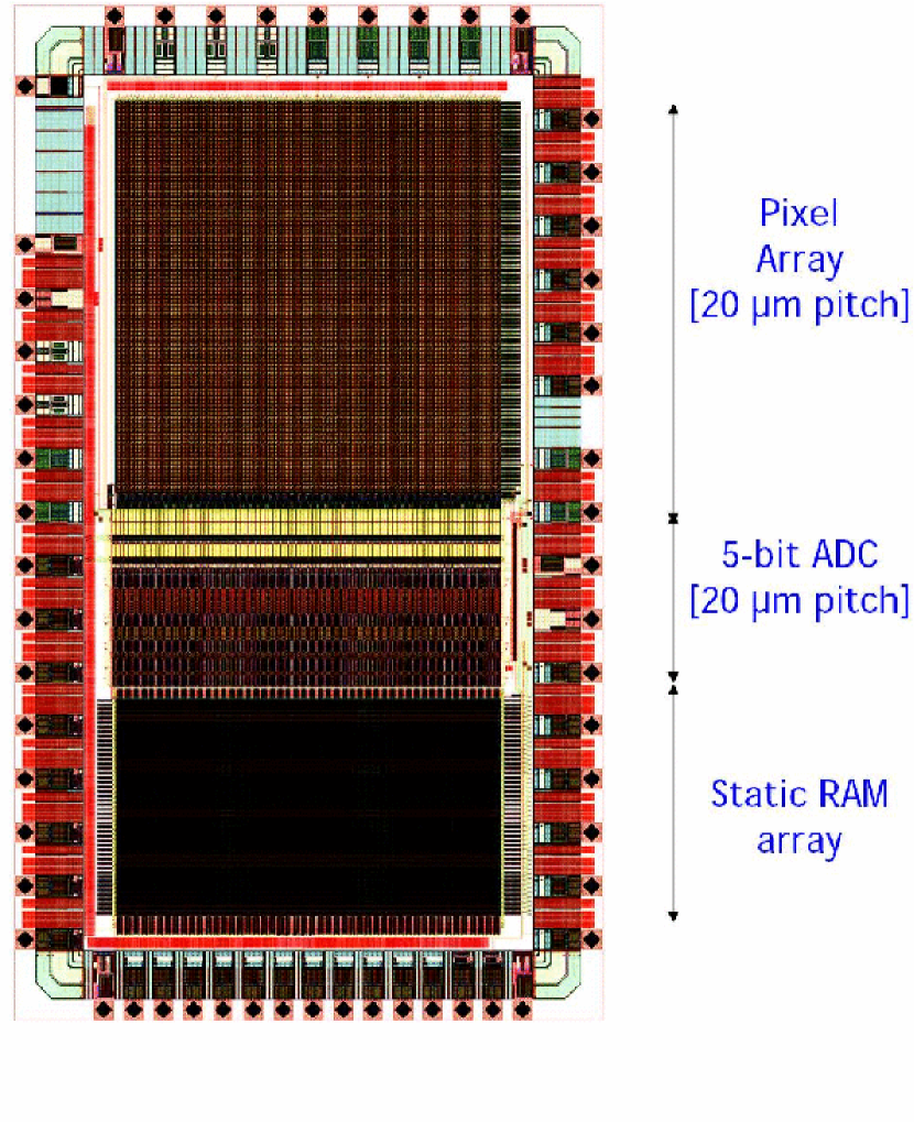
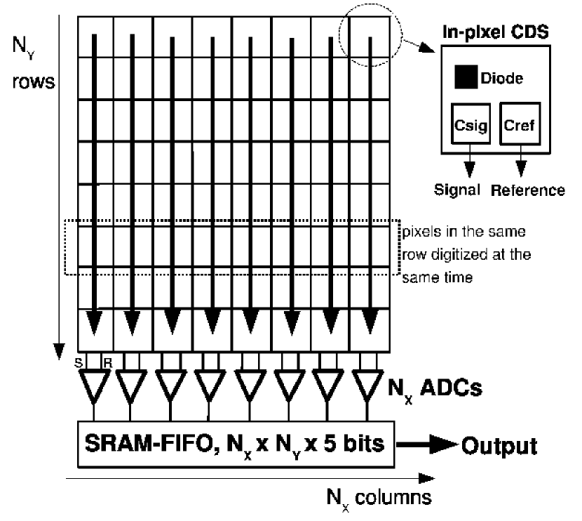
Figure 2 shows the chip layout and a sketch illustrating the chip working principle. The array consists of 9696 pixel of 20 m pitch. After a global reset, the sensor image is integrated, and then the pixel signal and reference levels are stored in the in-pixel capacitors. This is followed by a column-wise digitization of the pixel signals with concurrent storage in a SRAM-FIFO memory cell integrated at the bottom of the column. The digital image is then read out serially from the SRAM-FIFO using a 50 MHz clock. The chip is expected to be back from fabrication in October 2007.
3 SOI monolithic pixels
A first prototype chip has been designed and submitted in a 0.15 m fully-depleted SOI technology from OKI [4] in Fall 2006. The sensor is based on a 350 m thick high-resistivity substrate, separated by the CMOS circuitry by a 200 nm thick buried oxide. The CMOS circuitry is implanted on a 40 nm layer of silicon on top of the buried oxide. The thickness of this CMOS layer is small enough that the layer can be fully depleted. This technology is expected to combine the advantage of a depleted substrate with the possibility of integrating complex functionalities by making use of both types of MOS transistor, in contrast with standard CMOS monolithic APS which feature only -type transistors. Moreover, higher speed and lower power consumption can be achieved with the SOI process with respect to conventional CMOS processes.
The chip features 10 m pitch pixels, two analog sections with 1.0 V and 1.8 V bias and a digital section; all three sections are divided in 2 subsections with 11 and 55 m2 charge collecting diodes. The total array size is of 160150 pixels. The chip has been received back from foundry in May 2007. It is fully functional and is currently being tested.
4 Conclusions & Outlook
Recent progress in the development of the LDRD monolithic pixel chips at LBNL has been reviewed. A prototype with in-pixel CDS and fast readout has been successfully tested and will be used in June-July for tracking studies with 120 GeV protons at the MTBF facility at FNAL, in conjuction with the Thin Pixel Telescope described in [5]. Irradiation tests with 30 MeV protons and 1-20 MeV neutrons are also planned in Summer. The next prototype, implementing on-chip digitization, is expected in Fall 2007. In parallel, tests have started on a novel SOI chip, which combines a high-resistivity sensor substrate with a full CMOS circuitry implanted on top, so that higher circuitry complexity with low power dissipation can be implemented.
Acknowledgments
This work was supported by the Director, Office of Science, of the US Department of Energy under Contract no. DE-AC02-05CH11231.
References
-
[1]
Slides:
http://ilcagenda.linearcollider.org/contributionDisplay.py?contribId=302&sessionId=74&confId=1296 - [2] D. Contarato et al., Proceedings of the LCWS06 International Linear Collider Workshop 2006, Bangalore, India.
- [3] G. Deptuch et al., Nucl. Instrum. Meth. A 511 (2003) 240.
-
[4]
OKI Electric Industry Co., Ltd.,
http://www.oki.com - [5] M. Battaglia et al., Particle Tracking with a Thin Pixel Telescope, these Proceedings.