[D. N. Chigrin]Dmitry N. Chigrin111Corresponding author: e-mail: chigrin@th.physik.uni-bonn.de, Phone: +49 228 73 2046, Fax: +49 228 73 3223
[S. V. Zhukovsky]Sergei V. Zhukovsky
[A. V. Lavrinenko]Andrei V. Lavrinenko
[J. Kroha]Johann Kroha
Coupled nanopillar waveguides
Coupled nanopillar waveguides:
optical properties and applications
Abstract.
In this paper we review basic properties of coupled periodic and aperiodic nanopillar waveguides. A coupled nanopillar waveguide consists of several rows of periodically or aperiodically placed dielectric rods (pillars). In such a waveguide, light confinement is due to the total internal reflection, while guided modes dispersion is strongly affected by the waveguide structure. We present a systematic analysis of the optical properties of coupled nanopillar waveguides and discuss their possible applications for integrated optics.
keywords:
Coupled and nanopillar waveguides, periodic and aperiodic structures, photonics devicespacs Mathematics Subject Classification:
42.60.Fc, 42.55.Tv, 42.82.Gw.1. Introduction
Photonic crystals (PhCs) are known for offering unique opportunities for controling the flow of light by acting as waveguides, cavities, dispersive elements, etc [1, 2, 3, 4]. Photonic crystal waveguides (PCW) are one of the promising examples of PhCs applications at micron and sub-micron length-scales. They can be formed by removing one or several lines of scatterers from the PhC lattice (Fig. 1a). PCW based on PhCs with different two-dimensional (2D) lattices of both air holes in a dielectric background and dielectric rods in air were reported [1, 2, 3]. Light confinement in PCW is obtained due to a complete photonic bandgap (PBG), in contrast to the standard guiding mechanism in a conventional dielectric waveguide (Fig. 1b). It was theoretically predicted that a PhC waveguide can possess loss-free propagation as soon as a guiding mode falls into a complete PBG. However, progress in PhC research has revealed that losses are inevitable and sometimes might be rather high even in spite of broad PBG. Special optimization efforts are now intensively applied for decreasing optical losses and the results are quite promising [5, 6].
At the same time, PBG guiding is not the only waveguiding mechanism in a PhC. Unique anisotropy of PhCs can cancel out the natural diffraction of the light, leading to the self-guiding of a beam in a non-channel PCW [7, 8, 9]. The common principle of index guiding (guiding due to total internal reflection) can be also found in periodic systems. It is rather straightforward if a waveguide is organized as a defect in a lattice of holes in a dielectric material. Then, the channel itself has higher index of refraction than the average index of the drilled or etched medium. Topologically inverted systems like periodic arrays of rods or nanopillars placed in air can also provide waveguiding due to index difference [2]. However, fabrication of rod arrays on the nanoscale is a relatively difficult technological problem.
The recent progress in the fabrication of alternative structures, namely nanopillar waveguides (NPW), has proved the relevance of their study not only as a useful theoretical model. For example, two-dimensional (2D) silicon-on-insulator (SOI) pillar PhC have recently been fabricated and characterized [10]. Sandwich-like structures have also been successfully realized in material system [11]. Membrane-like structures have been realized, based on polymer membranes incorporating rods [12]. Recently, various combinations of active materials inserted in single nanowires or arrays of nanopillars have been under attention as well [13]. It is important to point out that all of the above mentioned studies do not only present a successful practical realization of the pillar PhC structures, but also report transmission efficiencies and out-of-plane radiation losses comparable with the 2D PhC based on hole geometry.
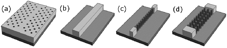
A one-dimensional (1D) chain of rods placed at equal distance from one another (Fig. 1c) possesses guiding properties as was shown by Fan et al. [2]. The fundamental mode of such a periodic nanopillar waveguide lies below the light line and below the first PBG corresponding to the 2D PhCs with a square lattice of the same rods. Guiding is due to total internal reflection. A better confinement of light can be achieved, if several 1D periodic chains are placed in parallel (Fig. 1d) [14]. Such waveguides are called coupled nanopillar waveguides (CNPWs) and are designated as Wn, where n is the number of parallel rows comprising the CNPW. In building a CNPW both the longitudinal and the transverse relative shift between individual waveguides can be arbitrary, and thus, a high flexibility in dispersion engineering can be achieved.
In this paper, we review basic properties of coupled nanopillar waveguides and discuss their possible applications for integrated optics. In Section 2, a CNPW is introduced and possible ways to tune the CNPW dispersion are discussed. The transmission efficiency of 2D and 3D CNPWs is reported in Section 3. The route to improve the coupling between a nanopillar waveguide and an external dielectric waveguide (like an optical fiber) is discussed in Section 4 with respect to aperiodic NPWs. Possible applications of coupled periodic and aperiodic nanopillar waveguides are discussed in Section 5. Section 6 concludes the paper.
2. Dispersion engineering
2.1. Dispersion tuning
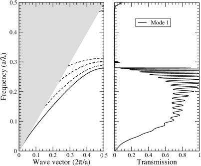
In reference [2] it was shown that a single row of periodically placed dielectric rods is effectively a single-mode waveguide within a wide frequency range (Fig. 2, left panel). It has a well confined fundamental mode. Attaching one, two or more identical W1 waveguides in parallel to the original one produces a coupled-waveguide structure [14]. It is well known in optoelectronics that this leads to the splitting of the original mode into n modes, where n is the number of coupled waveguides [15].
In Fig. 2, dispersion diagrams for W1, W2, W3 and W4 CNPWs are shown. All rods are placed at the vertices of a square lattice. To model a CNPW dispersion we used the plane-wave expansion method (PWM) [16]. The supercell consists of one period in the z direction and 20 periods in the x direction, where n periods occupied by dielectric rods were placed in the center of the supercell. The waveguide is oriented along the z-axis (Fig. 2). The calculations were performed for 2D structures and for TM polarization. The modes of the CNPW are bound between the and projected bands of the corresponding infinite PhC of a 2D square lattice of rods (Fig. 2, dashed lines) [14]. All modes are effectively localized within the waveguide region. Near the irreducible Brillouin zone (IBZ) boundary the dispersion is strongly affected by the system periodicity.
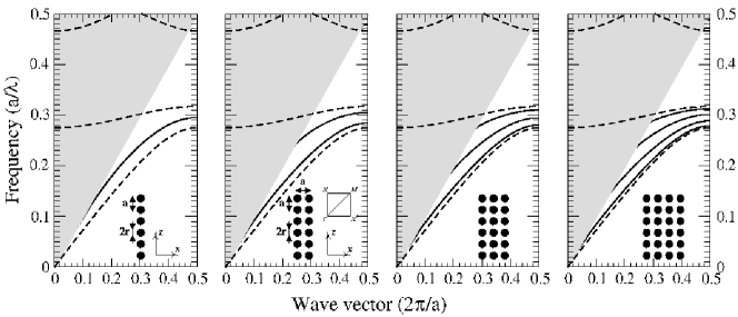
It is well known that by varying the filling factor, i.e. the rod radius, and the dielectric constant of the rods, one can tailor the frequency range and slope of the PhC bands. Taking into account that the CNPW modes are bound by and bands of the corresponding infinite 2D PhC, a proper frequency adjustment of nanopillar waveguide modes can be done by changing these two parameters. Decreasing the dielectric constant of the rods, while keeping their radius constant, pushes the bundle of n CNPW modes to higher frequencies. The modes shift towards lower frequencies, if the nanopillar radius increases, with fixed dielectric constant. In general, the mode tuning follows the rule: the larger the average refractive index of the system, the lower the mode frequencies [14].
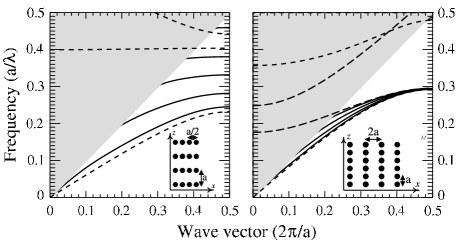
Another option for tuning the mode dispersion of CNPW is to change the distance between individual waveguides, the transverse offset. Examples are shown in figure 3 for two transverse offsets, (left) and (right). In these cases the rods are situated at the vertices of a rectangular lattice. While the mode overlap of individual waveguides is larger (smaller) for close (far) positioned waveguides, the coupling strength is stronger (weaker). For two identical waveguides, this in turn results in stronger (weaker) mode splitting, , with respect to the propagation constant of the uncoupled NPW. Here is a coupling coefficient [15]. Note, that the CNPW mode frequencies are still bounded by the position of the projected band structure of the corresponding infinite rectangular PhC (Fig. 3, dashed lines).
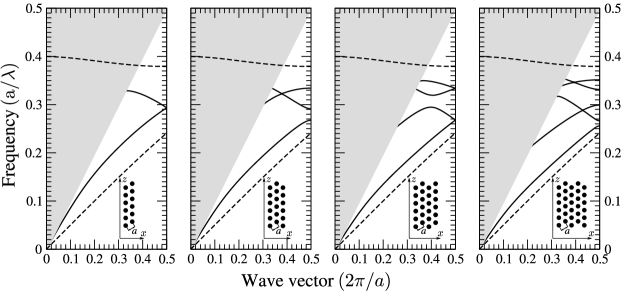
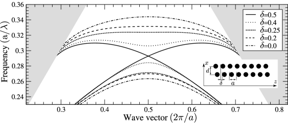
The last parameter which may affect the dispersion of a CNPW is the longitudinal shift between its individual rows. In figure 4 the dispersion diagrams for CNPW with rods placed in the vertices of a triangular lattice are shown for W2, W3, W4 and W5 waveguides. The orientation of the waveguides coincides with the direction of the triangular lattice. The mode splitting in a “triangular lattice” W2 waveguide strongly depends on the propagation constant (Fig. 4, left panel), being large for small and vanishing near the IBZ boundary. This is in contrast to a “square lattice” W2 waveguide (Fig. 2), where the mode splitting is approximately constant for all propagation constants. The mode multiplicity near the IBZ boundary leads to regions with negative dispersion (backward propagating waves) of the second mode. For CNPWs with the number of rods larger than two (Fig. 4, right panels) it results, furthermore, in the formation of mini-bandgaps and multiple backward waves regions in the dispersion. Note that in spite of the complex nature of the mode splitting, CNPW modes are still bounded by the projected bands of the corresponding triangular lattice PhC.
The longitudinal shift can be arbitrarily set to any value between and . The concomitant dramatic changes in the CNPW dispersion are illustrated in figure 5 for the case of W2 waveguide. Starting from the simple mode splitting for one can have a very flat second band for , with negative dispersion regions in the second band for and degenerate first and second bands at the IBZ boundary for . By combining such shifted W2 waveguides and appropriately chosing the rod radius and transverse offset one obtains large flexibility in designing CNPWs with anomalous dispersion in the frequency range of interest.
2.2. Coupled mode model
To understand qualitatively the physical mechanism of the anomalous dispersion presented in the last example (Fig. 5), the coupled mode theory (CMT) can be used [17]. Being an approximate theory, CMT nevertheless manages to combine a simple physical model with accurate qualitative and even quantitative results [18]. In what follows, two identical coupled periodic waveguides a-W1 and b-W1 are arranged in a W2 CNPW. The second waveguide, b-W1, is shifted by with respect to the first one (Fig. 5, inset). We limit ourselves to the scalar CMT, which in our case corresponds to the TM polarization.
The modes of the W2 waveguide are defined as the solutions of the 2D scalar wave equation
| (1) |
where the dielectric function of the composite structure is simply the sum of dielectric functions of the two W1 waveguides, . Here is a wave number in vacuum. We are looking for a solution of Eq. (1) in the form of a linear combination of the propagating modes of two isolated W1 waveguides [19], which allows us to separate spatial variables in the form
| (2) |
Here and are the slowly varying amplitudes of forward and backward propagating modes near the Bragg resonance condition of a single periodic W1 waveguide with period and . The functions and represent the transverse field distributions, and indexes refer to a-W1 and b-W1 waveguides, respectively. The spatial shift between the two W1 waveguides is accounted for by the corresponding phase shift of the field of the b-W1 waveguide. Here is the propagation constant of a homogenized W1 waveguide of width and dielectric constant . The dependence of the propagation constant on frequency is given by the standard planar waveguide dispersion relation [15]
| (3) |
where we have introduced the effective index of refraction of the homogenized waveguide . The transverse field distributions and obey the scalar wave equations
with and the transverse dependent dielectric functions being a z-average dielectric constant of the m-th waveguide. Substituting the mode expansion (2) into the scalar wave equation (1) and expanding the dielectric constant in a Fourier series with respect to ,
| (4) |
with the Fourier coefficients , one obtains after some lengthy but straightforward derivations a system of four ordinary differential equations relating slowly varying amplitudes of the forward and backward propagating modes in the two W1 waveguides,
| (5) |
For the propagation constant close to the Bragg point , the system matrix has the form
| (6) |
To simplify the following analysis, we have kept only two coupling constants, namely , accounting for the coupling between two homogenized waveguides, and , describing the waveguide’s intrinsic periodic structure. These coupling constants are defined in a usual way, as overlap integrals of the transverse field distributions with the corresponding Fourier coefficients of the dielectric function expansion. The resulting propagation constants of the supermodes of the W2 waveguide are given as the eigenvalues of the system matrix (6)
| (7) |
with
| (8) |
The implicit dependence of the propagation constant on frequency is given via the dispersion relation (3) of a planar homogenized waveguide.

In figure 6 the dispersion diagram of W2 waveguide calculated using Eqs. (7-8) is presented for three values of the longitudinal shift (left), (center) and (right). See figure caption for further details on the parameters. The dotted line shows the dispersion of a planar homogenized waveguide calculated using the dispersion relation (3) and folded back into the first Brillouin zone by the Bragg wave vector corresponding to the periodic W1 waveguide. By setting the self-action coupling constant, , to zero and choosing some finite value for the inter-row coupling constant, , one can reproduce the simple band splitting within the CMT model. The split modes are shown as dashed lines (Fig. 6).
To analyze the influence of the periodic structure and the longitudinal shift on the split band structure, we first consider zero longitudinal shift, . In this situation the detuning of the propagation constant from the Bragg wave vector, , is given by , where is the detuning of the propagation constant of the homogenized waveguide from the Bragg point. The propagation factor of the supermodes is given by the exponential , which corresponds to propagating modes only if . In the opposite situation, there are two bandgaps at Bragg wave vector with central frequencies corresponding to . These bandgaps are due to the destructive interference of the first forward propagating and the first backward propagating supermodes and the second forward propagating and the second backward propagating supermodes, respectively, as can be seen from the left panel of figure 6. In the case of half-period shifted W1 waveguides, , the detuning of the propagation constant and the supermode propagation constant are given by and . In this case two bandgaps exist at shifted Bragg wave vectors with central frequency at . This corresponds to the destructive interference of the first forward propagating and the second backward propagating supermodes and vice versa (Fig. 6, center). It is important to mention here that at the Bragg condition, , (IBZ boundary) the first forward propagating and the first backward propagating supermodes are in phase, which leads to the degeneracy of the first and second bands at the IBZ boundary (Fig. 4). The shift of the Bragg condition away from the IBZ boundary, , is a reason for the appearance of a region with negative dispersion in the second band (Fig. 4). In the case of arbitrary shift between the W1 waveguides a destructive interference takes place between all possible pair combinations of forward and backward propagating supermodes leading to the formation of four bandgaps and anomalous dispersion (Fig. 5). In the right panel of figure 6 an example of a CMT dispersion diagram is shown for the case of quarter-period shifted waveguides, .
3. Transmission efficiency
An important characteristic of the novel waveguides is their transmission efficiency. To analyze transmission efficiencies of different 2D and 3D CNPW, the finite difference time domain (FDTD) method [20] with perfectly matched layers as absorbing boundary conditions at all sides and a resolution of 16 grid points per lattice constant is used here. The modes are excited by a Gaussian-shaped temporal impulse, the Fourier transform of which is broad enough to cover the frequency range of interest. Fields are monitored by input and output detectors. The transmitted wave intensities are normalized by the ones of the incident waves.
The calculated transmission spectrum of a 20 periods long, straight “square-lattice” W4 CNPW is shown in the left panels of Fig. 7. There are four modes under the light line as it is shown in the band diagram. In Fig. 7 the transmission of the fundamental mode is shown directly together with the dispersion diagram. The W4 waveguide displays high transmission efficiency (close to 100%) over a broad spectral range. The position of the cut-off frequency is clearly seen in the spectrum.
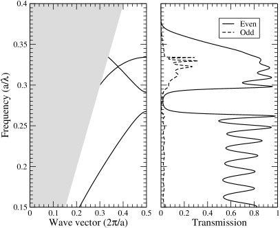
In the right panels of figure 7, the band structure and transmission spectra are shown for the W3 “triangular-lattice” CNPW. A 20 period long, straight CNPW is cut in the direction of the triangular lattice. A substantial suppression of the transmission is seen in the spectrum, coinciding exactly with the position of the mini bandgap in the band structure. Changing the parity of the signal field distorts the spectrum reflecting the mode symmetries. The even mode displays high transmission efficiency (close to 100%) over a broad spectral range. The odd mode has a lower level of transmission and is mostly transmitted at higher frequencies. Here, by odd and even modes we understand the corresponding first two fundamental modes of a conventional dielectric waveguide. The surprisingly high transmission of the even mode above the cutoff frequency, , can be explained by the resonant behavior of the folded radiation mode with negative group velocity [21]. We found similar behavior above cutoff for other “triangular-lattice” CNPW structures.
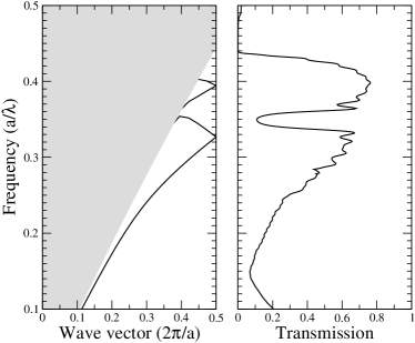
An example of 3D calculations for an SOI W4 “triangular-lattice” CNPW are presented in Fig. 8. In the left panel the dispersion diagram of the structure are presented, while its transmission spectrum for the even mode is plotted in the central panel. The dispersion diagram was calculated using 3D supercell PWM. In general, the transmission spectrum is very similar to the corresponding spectrum of 2D structure (Fig. 7, right). The transmission band is rather broad with 80% transmission efficiency at maximum and a sizable stopband at the mini bandgap frequencies. We attribute the moderate level of transmission to the impedance mismatch at the conventional waveguide–nanopillar waveguide interface. In the right panel of Fig. 8, the steady-state electric field distribution inside the CNPW is shown for a monochromatic source with normalized frequency . The field is well confined within the waveguide core in both the horizontal and vertical planes. there is no evidence for strong energy leakage into the substrate.
4. Aperiodic nanopillar waveguides
In addition to allowing arbitrary variation of the period and displacement (which is one of the advantages of the nanopillar waveguides as opposed to the PCWs), CNPWs allow arbitrary modification of the longitudinal geometry. A localized change of the properties introduced in one or several nanopillars would create a point defect, which functions as a resonator [2, 24]. The design of such micro-resonators on the scale of a few wavelengths is essential for integrated optics applications. Ideally, such resonators should combine the apparently contradictory features of a high Q-factor and of a sufficiently good coupling to a waveguide terminal to inject or extract light into or from the resonator. Due to the absence of a complete bandgap, the breaking of translational symmetry inevitably results in radiation losses of the resonator mode, which raises the need for optimizing the Q-factor of the resonator in 1D nanopillar waveguides. There have been some proposals to decrease the losses based on either mode delocalization [23] or on the effect of multipole cancellation [24]. A delocalized mode typically suffers from a decrease of the Q-factor. On the other hand, the spatial radiation loss profile of a mode described in Ref. [24] has a nodal line along the waveguide axis, which means poor coupling to any components coaxial with the waveguide.
Other than by means of a point defect, a resonant system can also be created by changing the periodic arrangement of nanopillars into a non-periodic one. We show that the use of such aperiodically ordered waveguide leads to improved coupling to the coaxial terminal without considerably sacrificing the Q-factor of the resonant modes. We use fractal Cantor-like NWPs as an example [25]. To construct aperiodic NPW, nanopillars of equal radius are arranged in a 1D chain, where the distances between adjacent pillars are given by the Cantor sequence. If we denote and for short and long distance ( and ), respectively, the Cantor sequence is created by the inflation rule and unfolds in the following self-similar fashion, which represents a series of middle third Cantor prefractals
In order to compare the amount of energy gathered by the coaxial terminal and dissipated elsewhere, we excite the system by a dipole source emitting a pulse with a broad spectrum, and use the FDTD method to investigate the process of energy loss into the surroundings. Fig. 9 shows the results. For the point-defect structure, the radiation of the resonant mode primarily escapes sideways (Fig. 9 (a)), so despite having a high -factor (), the coupling between the resonator and other components cannot be made efficient. The Cantor structure shows a considerably improved coupling (Fig. 9 (b)) accompanied by a drop of the -factor down to . Using a W3 CNPW with Cantor geometry (Fig. 9 (c)) raises it back to while still providing just as good coupling to the coaxial terminal.
One should notice that the Cantor geometry is only one kind of deterministically aperiodic arrangement. Other kinds, e.g., quasi-periodic Fibonacci-like one, can be used leading to a modification of the mode structure of NPWs as well as the coupling efficiency of resonant mode into coaxial terminal [25]. Engineering the longitudinal geometry of CNPWs appears to be a promising and powerful tool for a further degree of freedom in controlling the dispersion properties.
5. Applications
Relatively high transmission efficiency and flexibility in dispersion tuning of CNPWs may initiate their use as components for efficient and compact nanophotonic devices. Here we discuss two possible applications of CNPWs in integrated optics: a coupled nanopillar waveguide directional coupler [22] and a switchable coupled mode laser [31].
5.1. Directional coupler
A pair of CNPWs can be used as an effective directional coupler [22]. An example of such a directional coupler based on two W1 waveguides is shown in Fig. 10. Analyzing the dispersion diagram of the coupling section, namely W2 CNPW (Fig. 10, left panel), one can see a pronounced difference in the propagation constants of the even and odd supermodes in the frequency region around . It is a result of the strong interaction of coupled waveguides, which now are much closer to each other than in the case of standard line defect waveguides in a PhC lattice (see, for example, the similar rod structure in [26]). In this frequency range the difference between the even and odd supermode propagation constant is close to , which leads to a crude estimate of minimum coupling length [27]: Enhanced interaction leads to a shorter coupling length. This is illustrated in figure 10, right panel, where the time averaged squared electric field pattern is shown for the normalized frequency . Guided light hops from the bottom W1 waveguide to the top one and back on a distance equal to approximately , which represents well the estimated value. In contrast to a directional coupler proposed in [28], the CNPW structure does not require a specially adjusted separation layer between coupled waveguides, thus considerably simplifying a directional coupler design and fabrication.
There are several parameters, which can be used to optimize the directional coupler, e.g., length of the coupling region or the number of rows in each of the waveguides. As it has been shown in Sec. 2, longitudinal and transverse offsets between the individual waveguides, as well as variation of the dielectric constant and radius of the rods substantially modify the dispersion of the compound system, thus affecting the coupling efficiency. For example, by shortening the distance between two waveguides one can dramatically increase the propagation constant difference and reduce the coupler size. A similar effect cannot be achieved with standard PhC waveguides without any special design tricks involving intermediate walls, which increases the complexity of the fabrication procedure. An arbitrary longitudinal offset breaks the symmetry of the device with respect to the symmetry plane between the two W1 waveguides, which may further improve the coupling strength similar to the case of an antisymmetric grating coupler [29, 30].
5.2. Laser resonators
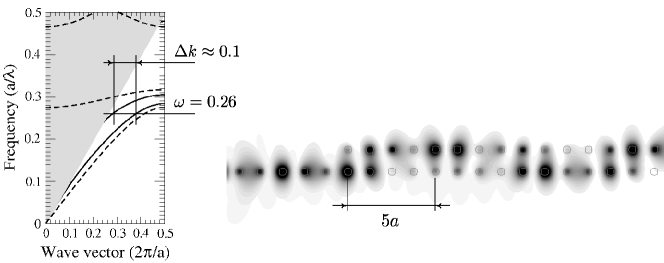
The periodicity of the coupled nanopillar waveguides can ensure the distributed feedback within a finite waveguide section. This can be seen from the flat tails of the nanopillar waveguide modes near the IBZ edge, which correspond to a very low group velocity of CNPW modes. Taking into account that any of the CNPW modes can be efficiently excited in the waveguide using an external seeding signal of the appropriate spatial profile [14], we have proposed the design of a switchable laser resonator [32] with distributed feedback based on the CNPW. The possibility to tune the number of modes, their frequency and separation (Sec. 2) would make such a resonator a promising candidate for a chip-integrated laser source.
The concept of switchable lasing was originally proposed in Ref. [14] and has got further justifications in our recent work [32]. In essence, a switchable microlaser comprised of a multimode microresonator, where lasing can be switched on demand to any of its eigenmodes by injection seeding [33, 34], i.e. by injecting an appropriate pulse before and during the onset of lasing, such that the stimulated emission builds up in a designated mode selected by this seeding field rather than from the random noise present in the system due to quantum fluctuations and spontaneous emission [32].
To provide a basic physical picture of switchable lasing we first consider briefly a simple semi-classical laser model in the case of two identical coupled single-mode cavities [32]. In this case there are two modes, the symmetric and the antisymmetric one, characterized by spatial field distributions and frequencies , respectively. Here is the mode detuning from the frequency of the single-cavity resonance, . For weak mode overlap the spatial intensity profiles of the two modes nearly coincide, . We assume that the cavities contain a laser medium with a homogeneously broadened gain line of width , centered at frequency . Here is the detuning of the gain profile from the cavity frequency . For this system the semiclassical Maxwell-Bloch equations [33, 35], in the rotating-wave and the slowly varying envelope approximation read
| (9) | |||||
Here all the spatial dependencies of the electric field and atomic polarization were represented in the basis of the two cavity modes, such that , etc., and the atomic polarization was eliminated adiabatically [36, 37]. are slowly varying envelopes of two modes . In Eqs. (9) the terms linear in describe stimulated emission driving, where the light-matter coupling constant is denoted by , the pumping rates projected onto the two resonator modes by , and the cavity mode decay rates by . Here is the dipole moment of the atomic transition. The coefficients , with , account for the different mode-to-gain couplings due to asymmetrical detuning of the atomic transition with respect to the resonator frequencies. The terms cubic in describe field saturation above the lasing threshold, where and the overlap integrals are taken over the regions containing the gain medium. Here is the non-radiative decay rate. The frequency dependence of the cross-saturation terms is given by , . Since we can further assume that , and .
The inhomogeneous terms originate from the external injection seeding field and from a noise field accounting for spontaneous emission [36]. For vanishing functions , Eqs. (9) would take the form of the standard two-mode competition equations [33, 35], describing bistable lasing [38] and mode hopping in the presence of stochastic noise in the system [39]. If both an external seeding field and a stochastic noise field are present in the cavity, , the inhomogeneous terms are given by,
| (10) |
The time integration in Eq. (10) is the averaging over a time interval larger than . The function is determined by the temporal dependence of the seeding signal . The coefficients and are determined by the spatial overlap of each mode with the seeding and noise fields, respectively.
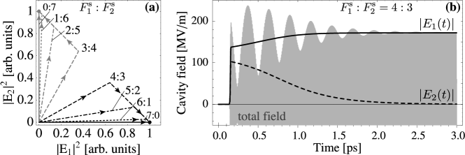
We consider the situation when the seeding prevails over the noise, i.e., , before and during the onset of lasing. After the onset the become so large that the terms have no effect anymore. In this situation the evolution of the resonator will be determined by the ratio of and . In Fig. 11 (left) the phase trajectories of the temporal resonator state evolution in the () space is presented for different values of and . As seen in Fig. 11 (left), the lasing state first reaches overall intensity saturation () and then drifts towards one of the stable fixed points corresponding to single-mode lasing (either or ). The drift happens on a longer time scale than the initial overall intensity growth, and the intermode beats decay fast after the lasing onset (Fig. 11, right). The drift occurs towards the mode whose spatial and temporal overlap with the seeding signal is larger, demonstrating a switchable lasing behavior. It is important to note that even in the case of asymmetric detuning of the cavity modes with respect to the gain frequency (), single-mode lasing is achieved into the mode whose spatial overlap with the seeding field, , is largest, i.e., if one of the following conditions, or , is satisfied.
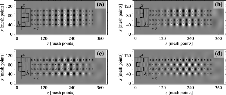
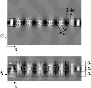
To demonstrate the predictions of this simple theory we have modeled the lasing action in four-row CNPW structure with a realistic injection seeding (Fig. 12) using the FDTD method [31]. The externally pumped laser-active medium is placed in the central 7 pillars of all four rows. This is done to maximize coupling between the active medium and the main localization region of the lasing modes. The population dynamics of an active medium is described at each space point by the rate equations of a four-level laser with an external pumping rate . To achieve population inversion we have chosen the following values for the non-radiative transition times, , with , , and the total level population is per unit cell [40]. The Maxwell equations are solved using FDTD scheme supplemented by the usual equation of motion for the polarization density in the medium and by the laser rate equations [41, 42, 40, 43]. All calculations were done for TM polarization. The seeding signal is excited by four emitters (linear groups of dipoles) engineered on the regular dielectric waveguide attached to the CNPW structure (see Fig. 12). Each of the emitters generates a single short Gaussian pulse with carrier frequency and with half-width duration . The relative phase of the fields in these pulses is chosen or . Technically, the seeding dipoles are realized as point like oscillating current sources in the Maxwell equations [31]. Similarly, the spontaneous emission [42, 44, 45] can be modeled as an ensemble of point current sources, randomly placed in space, with temporally -correlated Langevin noise [45]. The computational domain of size was discretized with a mesh point spacing of . The time step is related to the spatial mesh to assure stability and was chosen . To simulate an open system, perfectly matched layer (PML) boundary conditions [20] were used.
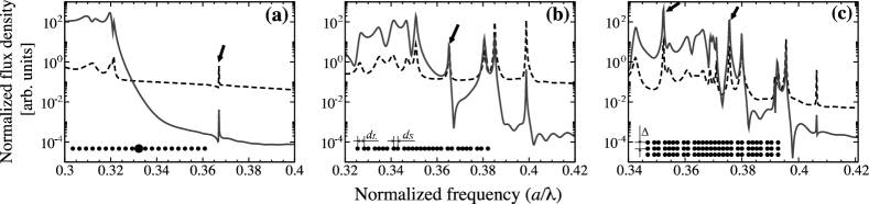
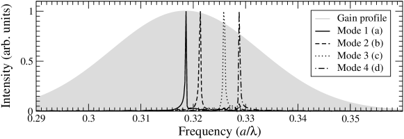
In Fig. 12 (top) the lasing spectra in the steady state long after the seeding signal has decayed is shown. The broad shaded areas depict the laser line of width centered at , which is shifted slightly towards lower frequencies. As a rule the -factor is larger for modes with the higher frequency. The shifted laser line compensates this -factor difference, so that any of the four CNPW modes can be selected by the appropriate seeding signal with the same symmetry. In figure 12 (bottom) the spatial electric field distribution in the four-row CNPW laser resonator is shown at an instant of time long after the seeding signal has decayed and after the steady state has been reached. The symmetry of the selected lasing modes corresponds to that of the seeding signal (Fig. 12).
The proposed concept of switchable lasing is not limited to the periodic CNPW structures, but is expected to work in any resonator featuring bi- or multistability. Any coupled cavity based system would be a good candidate for the effects predicted. For example aperiodic CNPW based resonator also show the switchable lasing behavior for resonant modes discussed in Sec. 4 [31].
6. Conclusion
We have shown that a novel type of coupled nanopillar waveguides, comprised of several periodic or aperiodic rows of dielectric rods, may have potential applications in compact photonics. The strong coupling regime can be utilized in ultrashort directional couplers or laser cavities, which might possess an additional functionality and flexibility when different longitudinal and transverse offsets among individual waveguides are employed. The factors of major influence upon the mode dispersion have been analyzed. Transmission spectra for 2D and 3D systems prove the possible single mode excitation by imposing specific symmetry conditions onto a field source and high transmission characteristics of coupled nanopillar waveguides.
DNC, SVZ and JK acknowledge partial support by the Deutsche Forschungsgemeinschaft through projects SPP 1113 and FOR 557. AVL acknowledges partial support by Danish Technical Research Council via PIPE project and the EU Commission FP6 via project NewTon (NMP4-CT-2005-017160).
References
- [1] J. D. Joannopoulos, R. D. Meade, and J. N. Winn, Photonic crystals: Molding the flow of light (Princeton U. Press, Princeton, N.J., 1995).
- [2] S. Fan, J. Winn, A. Devenyi, J. C. Chen, R. D. Meade, and J. D. Joannopoulos, “Guided and defect modes in periodic dielectric waveguides,” J. Opt. Soc. Amer. B, 12, 1267-1272 (1995).
- [3] S. G. Johnson, P.R. Villeneuve, S. Fan, and J. D. Joannopoulos, “Linear waveguides in photonic-crystal slabs,” Phys.Rev.B, 62, 8212-8222 (2000).
- [4] J. Opt. A 2001, V.3, No.6; Opt. Quant. Electron. 2002, V.34, No.1/3.
- [5] Y. Sugimoto, Y. Tanaka, N. Ikeda, T. Yang, H. Nakamura, K. Asakawa and K. Inoue, “Low propagation loss of 0.76 dB/mm in GaAs-based single-line-defect two-dimensional photonic crystal slab waveguides up to 1 cm in length,” Opt. Express, 12 1090, 2004.
- [6] M. Notomi, A. Shinya, S. Mitsugi, E. Kuramochi and H-Y. Ryu, “Waveguides, resonators and their coupled elements in photonic crystal slabs,” Opt. Express 12 1551, 2004.
- [7] D. N. Chigrin, S. Enoch, C. M. Sotomayor Torres, and G. Tayeb, “Self-guiding in two-dimensional photonic crystals,” Optics Express 11, 1203-1211 (2003).
- [8] J. Witzens and A. Scherer, “Efficient excitation of self-collimated beams and single Bloch modes in planar PhCs,” J. Opt. Soc. Amer. A 20, 935 (2003).
- [9] C. Chen, A. Sharkawy, D. M. Pustai, S. Shi, and D. W. Prather, “Optimizing bending efficiency of self-collimated beams in non-channel planar photonic crystal waveguides,” Optics Express 11, 3153-3159 (2003).
- [10] M. Tokushima, H. Yamada, and Y. Arakawa, “1.5 m-wavelength light guiding in waveguides in square-lattice-of-rod photonic crystal slab,” App. Phys. Lett. 84, 4298-4300 (2004)
- [11] S. Assefa, P. T. Rakich, P. Bienstman, S. G. Johnson, G. S. Petrich, J. D. Joannopoulos, L. A. Kolodziejski, E. P. Ippen, and H. I. Smith, “Guiding 1.5 m light in photonic crystals based on dielectric rods,” App. Phys. Lett. 85, 6110-6112 (2004)
- [12] E. Schonbrun, M. Tinker, W. Park, and J.-B. Lee, “Negative Refraction in a Si-Polymer Photonic Crystal Membrane,” IEEE Photonics Tech. Lett. 17, 1196-1198 (2005)
- [13] J. C. Johnson, H. Q. Yan, R. D. Schaller, L. H. Haber, R. J. Saykally and P. D. Yang, “Single Nanowire Lasers,” J. Phys. Chemistry B 105 11387 (2001)
- [14] D. N. Chigrin, A. V. Lavrinenko, C. M. Sotomayor Torres, “nanopillar photonic crystal waveguides,” Opt. Express, vol. 12 , 617-622 (2004)
- [15] L. A. Coldren and S.W.Corzine. “Diode lasers and photonic integrated circuits,” (John Wiley, New York, 1995)
- [16] S. G. Johnson and J. D. Joannopoulos, “Block-iterative frequency-domain methods for Maxwell’s equations in a planewave basis,” Opt. Express 8, 173 (2001)
- [17] A. V. Lavrinenko and D. N. Chigrin, “Coupled mode theory of shifted periodic waveguides” (unpublished)
- [18] W. P. Huang, “Coupled mode theory for optical waveguides: An overview,” J. Opt. Soc. Amer. A 11, 963-983 (1994)
- [19] R. März and H. P. Nolting, “Spectral properties of asymmetrical optical directional couplers with periodic structures,” Opt and Quantum Electron. 19, 273-287 (1987)
- [20] A. Lavrinenko, P. I. Borel, L. H. Fradsen, M. Thorhauge, A. Harpoth, M. Kristensen, T. Niemi, and H. M. H. Chong, “Comprehensive FDTD modelling of photonic crystal waveguide componets,” Opt.Express 12, 234-248 (2004)
- [21] M. Loncar, D. Nedeljkovic, T. P. Pearsall, J. Vuckovic, A. Scherer, S. Kuchinsky, D. C. Allan, “Experimental and theoretical confirmation of Bloch-mode light propagation in planar photonic crystal waveguides,” Appl. Phys. Lett. 80, 1689-1691 (2002).
- [22] D. N. Chigrin, A. V. Lavrinenko and C. M. Sotomayor Torres, “Numerical characterization of nanopillar photonic crystal waveguides and directional couplers,” Opt. and Quanum Electron. 37, 331 (2005)
- [23] H. Benisty, D. Labilloy, C. Weisbuch, C. J. M. Smith, T. F. Krauss, D. Kassagne, A. Béraud, C. Jouanin, Radiation losses of waveguide-based two-dimensional protonic crystals: Positive role of the substrate, Appl. Phys. Lett. 76, 532–534 (2000)
- [24] S. G. Johnson, S. Fan, A. Mekis, J. D. Joannopoulos, Multipole-cancellation mechanism for high- cavities in the absence of a complete photonic band gap, Appl. Phys. Lett. 78, 3388–3390 (2001)
- [25] S. V. Zhukovsky, D. N. Chigrin, and J. Kroha, “Low-loss resonant modes in deterministically aperiodic nanopillar waveguides,” J. Opt. Soc. Am. 10 2256-2272 (2006)
- [26] S. Boscolo, M. Midrio and C. G. Somedo. “Coupling and decoupling of electromagnetic waves in parallel 2D photonic crystal waveguides,” IEEE J. Quantum Electron. 38, 47 (2002)
- [27] J. Zimmermann, M. Kamp, A. Forchel and R. Marz, “Photonic crystal waveguide directional couplers as wavelength selective optical filters,” Optics Communic. 230, 387 (2004)
- [28] A. Martinez, F. Cuesta and J. Marti, “Ultrashot 2D photonic crystal directional couplers,” IEEE Photon. Technol. Lett. 15, 694 (2003)
- [29] G. Perrone, M. Laurenzanno and I. Montrosset, “Design and feasibility analysis of an innovative integrated grating-assisted add-drop multiplexer,” J. Lightwave Technol. 19, 1943 (2001)
- [30] M. Aslund, J. Canning, L. Poladian, C. M. de Sterke and A. Judge, “Antisymmetric grating coupler: experimental results,” Appl. Opt. 42, 6578 (2003)
- [31] S. V. Zhukovsky, D. N. Chigrin, A. V. Lavrinenko and J. Kroha, “Selective lasing in multimode periodic and non-periodic nanopillar waveguides,” Phys. Stat. Sol. b (in press)
- [32] S. V. Zhukovsky, D. N. Chigrin, A. V. Lavrinenko and J. Kroha, “Switchable lasing in coupled multimode microcavities,” cond-mat/0701619 (submitted for publication)
- [33] A. Siegman, Lasers (University Science Books, Mill Valley, CA, 1986)
- [34] W. Lee and W. R. Lempert, Appl. Opt. 42, 4320 (2003)
- [35] M. Sargeant III, M. O. Scully, W. E. Lamb, Jr., Laser Physics (Addison-Wesley, Reading, MA, 1974)
- [36] S. E. Hodges, M. Munroe, J. Cooper, and M. G. Raymer, “Multimode laser model with coupled cavities and quantum noise,” J. Opt. Soc. Am. B 14, 191-197 (1997)
- [37] L. Florescu, K. Busch, and S. John, “Semiclassical theory of lasing in photonic crystals,” J. Opt. Soc. Am. B 19, 2215-2223 (2002)
- [38] G. P. Agrawal and N. K. Dutta, “Optical bistability in coupled-cavity semiconductor lasers,” J. Appl. Phys. 56 664-669 (1985)
- [39] J. Bang, K. Blotekjar and R. Ellingsen, “Computer-simulations of bistable dynamics of a 2-mode laser with symmetrical or asymmetrical gain conditions,” IEEE J. Quant. Electron. 27, 2356-2363 (1991)
- [40] S.-H. Chang and A. Taflove, “Finite-difference time-domain model of lasing action in a four-level two-electron atomic system,” Opt. Express 12, 3827-3833 (2004)
- [41] A. S. Nagra and R. A. York, FDTD analysis of wave propagation in nonlinear absorbing and gain media,” IEEE Trans. Ant. Propag. 46, 334- (1998)
- [42] X. Jiang and C. M. Soukoulis, “Time Dependent Theory for Random Lasers,” Phys. Rev. Lett. 85, 70-73 (2000)
- [43] P. Bermel, A. Rodriguez, S. G. Johnson, J. D. Joannopoulos, and M. Soljacic, “Single-photon all-optical switching using waveguide-cavity quantum electrodynamics,” Phys. Rev. A 74, 043818 (2006)
- [44] M.-K. Seo, G. H. Song, I.-K. H., and Y.-H. Lee, “Nonlinear dispersive three-dimensional finite-difference time-domain analysis for photonic-crystal lasers," Opt. Express 13, 9645-9651 (2005)
- [45] G. M. Slavcheva, J. M. Arnold, and R. W. Ziolkowski, “FDTD simulation of the nonlinear gain dynamics in active optical waveguides and semiconductor microcavities,” IEEE J. Sel. Top. Quant. Electron. 10, 1052-1062 (2004)