A Monolithic Pixel Sensor
in 0.15 m Fully Depleted SOI Technology
Abstract
This letter presents the design of a monolithic pixel sensor with 1010 m2 pixels in OKI 0.15 m fully depleted SOI technology and first results of its characterisation. The response of the chip to charged particles has been studied on the 1.35 GeV beam at the LBNL ALS.
keywords:
Monolithic pixel sensor; SOI; CMOS technology; Particle detectionSilicon on insulator (SOI) technology allows to fabricate CMOS circuits on a thin Si layer, electronically insulated from the rest of the wafer. The isolation of the electronics from the detector volume offers clear advantages for designing monolithic pixel sensors for particle detection, compared to MAPS pixel devices, realised in standard CMOS bulk process. First both nMOS and pMOS transistors can be built, without disturbing the charge collection, and then the detector wafer can be biased thus improving the efficiency of charge carriers collection. There have been already attempts of developing SOI pixel sensors for charged particle detection with a high resistivity bottom wafer. The first used a 3 m process at IET, Poland and gave a proof of principle of the concept soi-iet1 ; a test structure with 150150 m2 pixels observed signals of low-momentum electrons from a 90Sr source soi-iet3 . The availability of the 0.15 m FD-SOI process by OKI Electric Industry Co. Ltd. Japan, has opened up new possibilities for SOI pixel sensors with the pixel pitch required for the next generation of particle physics experiments and imaging.A chip based on this process has already been designed by a group at KEK, Japan and successful tested with an IR laser beam soi-oki2 .
We designed and submitted a monolithic pixel sensor chip, with 1010 m2 pixels, for detection of charged particles. This letter presents the chip design, results of its characterisation and the first signal of high momentum particles, obtained with the 1.35 GeV electrons beam from the LBNL Advanced Light Source (ALS) booster.
The sensor has a 350 m thick high-resistivity substrate, the CMOS circuitry is implanted on a 40 nm Si layer on top of a 200 nm thick buried oxide.
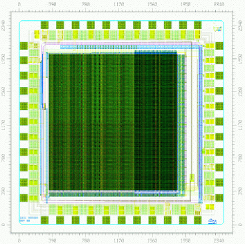
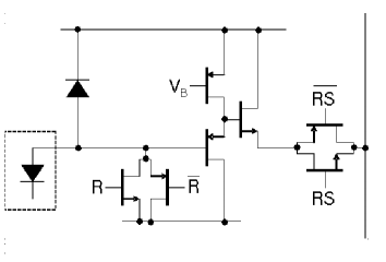
The thickness of the CMOS layer is small enough for the layer to be fully depleted. The chip features an array of 160150 pixels on a 10 m pitch. The OKI SOI technology includes thin-oxide 1.0 V transistors and thick-oxide 1.8 V transistors. The left-most 50 columns are simple analog pixels constructed with 1.0 V transistors. The centre 50 columns are constructed with 1.8 V pixels, and the right-most 50 columns are clocked, digital pixels. The 1.0 V pixels have significantly higher leakage currents than the 1.8 V pixels, which will be seen later to affect the signal-to-noise ratio. The schematic for the analog pixels is shown in Figure 2. The operation is comparable to a conventional 3T pixel, except that an internal source follower has been added in order to minimise kickback from the row select switches.
Each sector is divided in two subsections with 11 and 55 m2 charge collecting diodes. Single transistor test structures have been implemented at the chip periphery, including complementary -type and -type MOSFETs, all with =50 m and =0.3 m, with different types of body contacts (floating, source-tied and gate-tied).
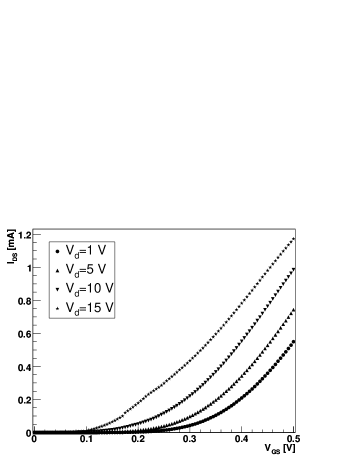
The transistor characteristics have been studied as a function of the sensor substrate bias, , in order to evaluate possible back-gating effects, which are expected to be significant due to the relatively small thickness of the buried oxide. Figure 3 shows the input characteristics measured at different substrate biases for a nMOSFET with =50 m and =0.3 m, with floating body contact. The measurements are performed with the transistor biased in saturation region. The threshold voltages shift from 0.24 V at =1 V to 0.07 V at =15 V, consistent with an increased back-gating effect.
Each 8000-pixel analog section is read out independently using a 14-bit ADC. A Xilinx FPGA controls all pixel clocks and resets. The pixels are clocked at 6.25 MHz giving an integration time of 1.382 ms. Correlated double sampling is performed by acquiring two frames of data with no pixel reset between the readings and subtracting the first frame from the second. The response of the analog sections has been tested with an 1060 nm IR laser, for different values. The laser is focused to a 20 m spot and pulsed for 30 s between successive readings. We measure the signal pulse height in a 55 matrix, centred around the laser spot centre. The measured signal increases as , as expected from the increase of the depletion region, until 9 V, where it saturates, to decrease for 15 V.
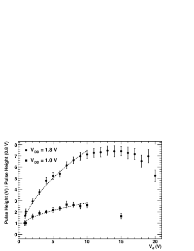
We interpret this effect as due to the transistor back-gating and affects the 1.0 V transistor pixels at lower values of . The pixel chip has been tested on the 1.35 GeV electron beam-line at LBNL ALS. The readout sequence is synchronised with the 1 Hz booster extraction cycle so that the beam spill hits the detector just before the second frame is read. The temperature is kept constant during operation at 23∘C by forced airflow. Only the analog part of the chip is readout. All the sections are functional and here we report results for two of the analog sections, with =1.0 V and 1.8 V transistors respectively, each consisting of a 0.40.8 mm2 active region. Data are processed on-line by a LabView-based program, which performs correlated double sampling, pedestal subtraction and noise computation. The data is converted in the lcio format and the offline analysis is performed using a set of dedicated processors developed in the Marlin framework Gaede:2006pj .
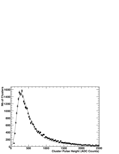
Each event is scanned for seed pixels with pulse height above a signal-to-noise (S/N) threshold of 4.5. Noisy pixels are flagged and masked. Seeds are sorted according to their pulse heights and the neighbouring pixels in a 55 matrix with S/N2.5 are added to the cluster. Clusters are not allowed to overlap and we require that pixels associated to a cluster are not interleaved by any pixels below the neighbour threshold. The average number of pixels accepted in a cluster is given in Table 1. Only clusters with at least two pixels are further considered for the analysis. Data have been taken at different depletion voltages, , from 1 V up to 20 V. Control data sets were taken under the same conditions but without beam, to monitor the effect of noisy pixels. Results are summarised in Table 1. There is only a small background arising from noisy pixels, which survives the bad pixel cut and the cluster quality criteria. Figure 5 shows the cluster pulse height for data taken with = 10 V. The pixel multiplicity in a cluster decreases with increasing depletion voltage while the cluster pulse height increases up to 10 V. At 15 V the cluster signal and the efficiency of the chip decreases, as observed in the laser test.
| Nb Pixels | Signal MPV | S/N | ||||||||
|---|---|---|---|---|---|---|---|---|---|---|
| (V) | beam on | beam off | in Cluster | (ADC Counts) | ||||||
| 1.0V | 1.8V | 1.0V | 1.8V | 1.0V | 1.8V | 1.0V | 1.8V | 1.0V | 1.8V | |
| 1 | 3.9 | 9.7 | 0.02 | 0.05 | 2.67 | 3.31 | 105. | 132 | 7.4 | 8.9 |
| 5 | 6.7 | 14.0 | 0.03 | 0.12 | 2.54 | 3.39 | 140. | 242 | 8.8 | 14.9 |
| 10 | 4.4 | 7.8 | 0.03 | 0.20 | 2.41 | 3.31 | 164. | 316 | 8.1 | 15.0 |
| 15 | 1.4 | 3.9 | 0.02 | 0.01 | 2.02 | 2.45 | 123. | 301 | 6.5 | 13.6 |
The depletion voltages used correspond to an estimated depletion thickness from 8 m to 56 m for = 1 V to 15 V. The section with 1.8 V transistors exhibits a good signal-to noise ratio for 5 V15 V. These results are very encouraging for the further development of monolithic pixel sensors in SOI technology.
Acknowledgements
This work was supported by the Director, Office of Science, of the U.S. Department of Energy under Contract No.DE-AC02-05CH11231. We are indebted to the ALS staff for their assistance and the excellent performance of the machine.
References
- (1) J. Marczewski et al., Nucl. Instrum. Meth. A 549 (2005) 112.
- (2) H. Niemiec et al., Nucl. Instrum. Meth. A 568 (2006) 153.
- (3) T. Tsuboyama et al., to appear on Nucl. Instrum. Meth. A (2007).
- (4) F. Gaede, Nucl. Instrum. Meth. A 559 (2006) 177.