Raman imaging of doping domains in graphene on SiO2
Abstract
We present spatially resolved Raman images of the G and 2D lines of single-layer graphene flakes. The spatial fluctuations of G and 2D lines are correlated and are thus shown to be affiliated with local doping domains. We investigate the position of the 2D line – the most significant Raman peak to identify single-layer graphene – as a function of charging up to cm-2. Contrary to the G line which exhibits a strong and symmetric stiffening with respect to electron and hole-doping, the 2D line shows a weak and slightly asymmetric stiffening for low doping. Additionally, the line width of the 2D line is, in contrast to the G line, doping-independent making this quantity a reliable measure for identifying single-layer graphene.
pacs:
63.20.K-, 78.30.-j, 78.30Na, 81.05.-t, 81.05.UwGraphene has attracted increasing attention over the last few years gei07 ; kat07 . Its unique electronic properties nov05 ; zha05 , mainly due to the linear energy vs. momentum dispersion and the electron hole symmetry near the charge neutrality point, makes it an interesting nanomaterial for high mobility electronics che07 ; han07 . Raman spectroscopy has proven to be a powerful tool to distinguish single-layer graphene from few-layer graphene and graphite fer06 ; gupta ; dav07a ; fer07 ; gra07b . The particular electronic structure of graphite and graphene leads to Kohn-anomalies in the phonon dispersion at the and points pis04 ; pis06 . At , the Born-Oppenheimer approximation, which is usually employed for the calculation of phonon frequencies, is no longer valid because of the Kohn-anomaly lazzeri . This leads to a pronounced stiffening of the Raman G line upon positive or negative charging (p or n-doping) of the graphene sheet ando ; pis07 ; yan07 . In this paper, we investigate how spatially resolved Raman spectroscopy can be used to probe doping domains and local charge fluctuations. While electron-hole puddles (i.e. local charge fluctuations) have been predicted to be responsible for the finite conductance at vanishing (average) charge carrier density hwang and have recently been observed using a scanning single electron transistor mar07 , the identification of different doping domains might be desirable to investigate novel graphene devices. Here, we report on Raman measurements on back gate induced charged graphene and on Raman imaging of doping fluctuations of isolated graphene flakes. We focus on the correlation between the shifts of the G line and the 2D line (or D∗ line). The latter one is the most significant Raman peak in single-layer graphene fer06 ; dav07a . Within the low charging regime (up to cm-2) obtained in our experiments, the 2D line stiffens for both electron and hole charging while its line width (in contrast to the G line) is not affected by charging. A good correlation between the shift of G and 2D lines is observed. However, the spectral resolution and lateral resolution are not sufficient to resolve electron-hole puddles as shown in Ref. mar07 . Therefore we refer to charging (i.e. doping) domains rather than to local electron-hole puddles.
We present both Raman images of isolated graphene and Raman measurements on electrically contacted single-layer graphene on 300 nm SiO2, where highly doped Si is used as back gate. The samples are prepared by micromechanical cleavage dav07b and Raman imaging sta07a is used to select single-layer graphene flakes fer06 ; dav07a . By electron-beam lithography we pattern scanning force microscopy

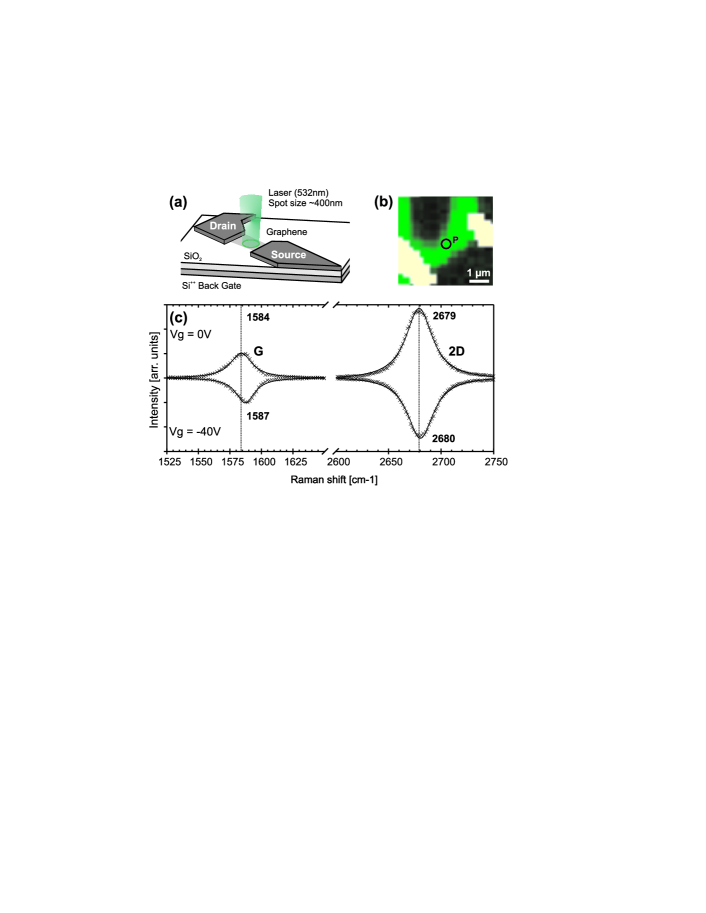
pre-mapped electrodes (5 nm Cr/60 nm Au) on the graphene flakes, which finally allows to apply a back gate voltage between the Si++ substrate and graphene. The experimental setup is shown in Fig. 1(a). The Raman data are recorded by using a laser excitation of 532 nm (=2.33 eV) through a single-mode optical fiber, whose spot size is limited by diffraction. A long working distance focusing lens with numerical aperture of approx. 0.80 is used to obtain a spot size of approx. 400 nm. We use a laser power below 2 mW such that heating effects can be neglected jun07a . A Raman image of a measured device is shown in Fig. 1(b) and the Raman spectra corresponding to point P (Fig. 1(b)) for a charged and charge-neutral case are plotted in Fig. 1(c). The G line shifts approx. by 3 cm-1 due to hole charging (of cm-2) and a corresponding (hardly visible) small shift in the 2D line is observed, too.

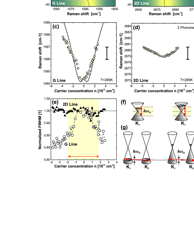
Fig. 2 shows Raman data for varying back gate voltages (Figs. 2(a,b)), which by utilizing a simple capacitor model can be substituted by the electron/hole concentration . Here cm-2/V nov05 and V marks the charge neutrality point, which has been determined by transport measurements. A typical back gate characteristic of the investigated device is shown in Fig. 4 in Ref. mol07b . The symmetric hole and electron charging-dependent stiffening of the -phonon was recently explained as the effect of non-adiabaticity lazzeri ; ando ; pis07 ; yan07 , i.e., the fact that the time-scale of phonon oscillations in graphite is not long compared to the electron relaxation time (see e.g. Eq. (6) in Ref. pis07 , and dashed line in Fig. 2(c)). Results of time-dependent perturbation theory were, however, so far only presented for phonons at the point. For the phonon between and which is responsible for the 2D line, it has been argued ferrari07a that non-adiabatic effects are negligible and the influence of charging can be reproduced by a standard adiabatic phonon calculation. While non-adiabatic calculations predict a phonon stiffening for hole-doping and a phonon softening for electron-doping ferrari07a ; tobepubl , we observe (see Fig. 2(d)) a slight (asymmetric) stiffening for both electron and hole-doping in agreement with the measurements of Ref. yan07 .
Another significant difference between the G and 2D lines is their line width (FWHM, shown in Fig. 2(e)). The G phonon () shows a rather strong change as function of carrier density yan07 ; pis07 which is due to the fact that the Pauli exclusion principle prevents the phonon from decaying into an electron-hole pair for , as illustrated in Fig. 2(f) yan07 . The decay of the dispersive D phonon with large wave vector is unaffected by the Pauli exclusion principle for low doping (Fig. 2(g)). It is expected that the 2D line width stays constant up to a charging that corresponds to a Fermi level shift as large as the exciting laser energy . This has a practical implication: Since the peak width of the 2D line, which has been recognized as the most striking feature to distinguish single-layer from few-layer graphene fer06 ; gupta ; dav07a , is insensitive to doping, it is a reliable - doping-independent - measure for identifying single-layer graphene.

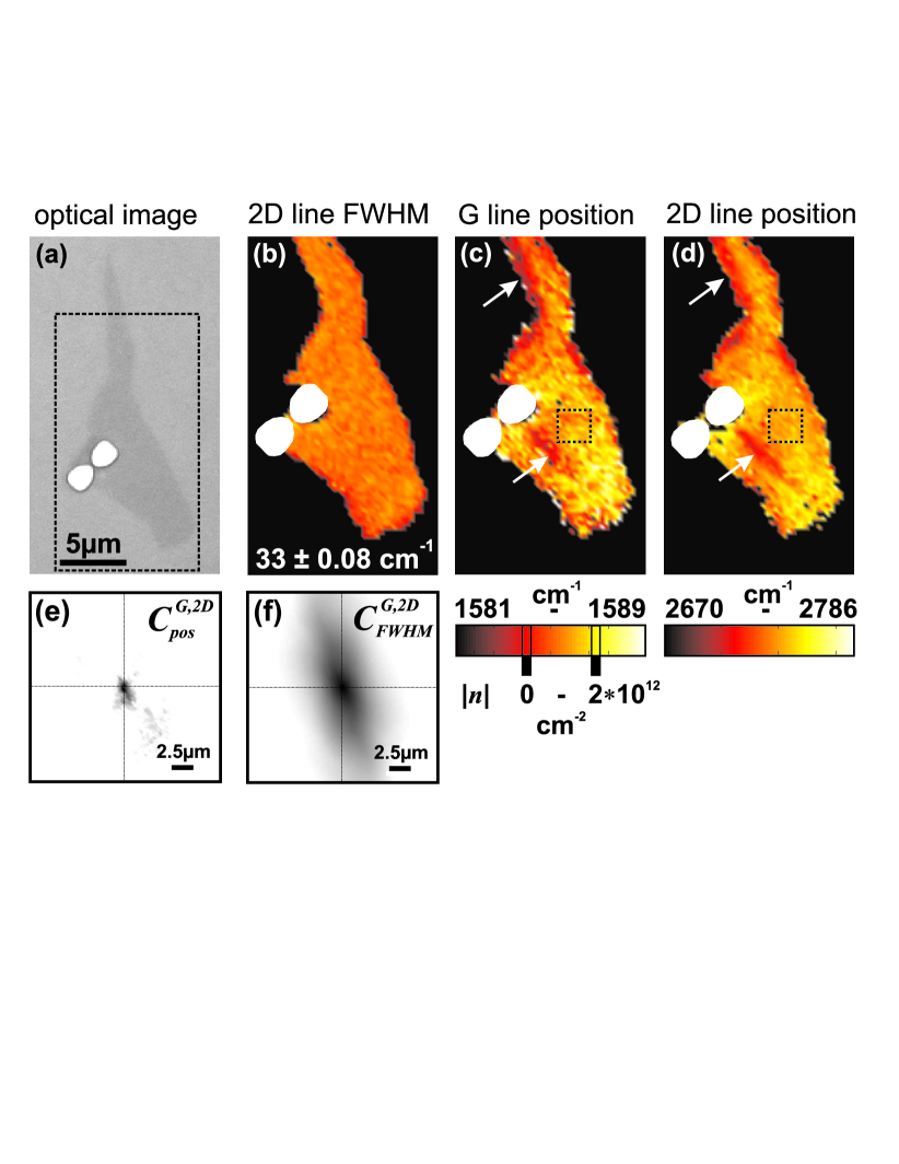
Spatially resolved Raman spectroscopy (Raman imaging) sensing the doping-dependent G and 2D line shifts provides an interesting tool to investigate charge fluctuations and doping domains in graphene. Here we present an example of Raman images (80x45 pixels) of a graphene flake on SiO2 (Fig. 3), where most attention has been paid to the G and 2D peak positions and widths, their fluctuations and cross-correlations. The average G peak position (Fig. 3(c)), , measured on the flake shown in Fig. 3(a), is 1585.4 cm-1 and the root mean square (RMS) of the peak fluctuations is 3.3 cm-1. This fluctuation also nicely explains the wide spread range of reported in the literature fer06 ; gupta ; dav07a ; fer07 ; gra07b . The 2D line (Fig. 3(d)) is centered around 2679.4 cm-1 and fluctuates with 0.9 cm-1. The ratio of the fluctuations of the G and 2D line agrees well with the ratio of the doping-dependent G and 2D stiffening (Figs. 2(c,d)) of 3.2. In Figs. 3(c,d) doped regions on the imaged flake can be observed gra07b . In the upper part we see that towards the edges of the graphene sample charging is suppressed, whereas in the entire inner area significant charging is present. Focusing on a quite uniform area (dotted box in Figs. 3(c,d)) we find that the -fluctuations are approx. cm-1, which corresponds to cm-2. Please note, that the local charge fluctuations due to electron-hole puddles presented in Ref. mar07 are by one order of magnitude smaller in amplitude and have been measured at low temperature and controlled environment. In addition, our lateral resolution is limited by the laser spot size. Figs. 3(c,d), however, nicely illustrate the correlation of G and 2D fluctuations (see e.g. white arrows). This can be also expressed by the two-dimensional cross-correlation function , which exhibits a clear narrow central peak (Fig. 3(e)). In contrast does show no measurable correlation of the width of G and 2D (Fig. 3(f)) as expected, since they are uncorrelated quantities. Indeed the FWHM of the 2D line does not exhibit any doping dependence as shown in Fig. 3(b). The line width of the 2D line stays constant at 330.08 cm-1 testifying its good quality for identifying single-layer graphene.
In summary, we have presented Raman shifts of the G and 2D line for back gate induced charged graphene. We have discussed the spatial variations in the G and 2D peak positions which can be attributed to different doping domains. In the low doping regime no clear distinction between electron and hole-doping can be made since for both G and 2D line, stiffening is observed. However, absolute doping fluctuations can be estimated. This technique is promising to investigate, e.g., electric field distributions in (side) gated graphene devices mol07 .
Acknowledgment — The authors wish to thank A. Bürli, S. Pisana, A. C. Ferrari, C. Roman, T. Helbling, A. Rubio, M. Lazzeri, and F. Mauri for helpful discussions. Support by the ETH FIRST Lab and financial support by the TH-18/03-1 grant, Swiss National Science Foundation (20021-108059/1) and NCCR nanoscience are gratefully acknowledged. L.W. acknowledges support from the French National Research Agency.
Note added — During completion of the manuscript, we became aware of a quite similar work ferrari07b in which doping-dependent fluctuations and a correlation between the position of G and 2D line are observed during non-spatially resolved measurements on many different graphene flakes.
References
- (1) A. K. Geim and K. S. Novoselov, Nat. Mater. 6, 183 (2007).
- (2) M. I. Katsnelson, Materials Today 10(1-2), 20 (2007).
- (3) K. S. Novoselov, A. K. Geim, S. V. Morozov, D. Jiang, M. I. Katsnelson, I. V. Grigorieva, S. V. Dubonos, and A. A. Firsov, Nature 438, 197 (2005).
- (4) Y. Zhang, Y.-W. Tan, H. L. Stormer, and P. Kim, Nature 438, 201 (2005).
- (5) Z. Chen, Y. Lin, M. Rooks and P. Avouris, cond-mat/0701599 (2007).
- (6) M. Y. Han, B. Özyilmaz, Y. Zhang, and P. Kim, Phys. Rev. Lett., 98, 206805 (2007).
- (7) A. C. Ferrari, J. C. Meyer, V. Scardaci, C. Casiraghi, M. Lazzeri, F. Mauri, S. Piscanec, D. Jiang, K. S. Novoselov, S. Roth, and A. K. Geim, Phys. Rev. Lett. 97, 187401 (2006).
- (8) A. Gupta, G. Chen, P. Joshi, S. Tadigadapa, and P. C. Eklund, Nano Lett. 6, 2667 (2006).
- (9) D. Graf, F. Molitor, K. Ensslin, C. Stampfer, A. Jungen, C. Hierold, and L. Wirtz, Nano Lett. 7, 238 (2007).
- (10) A. C. Ferrari, Solid State Commun., 143, 47 (2007).
- (11) D. Graf, F. Molitor, K. Ensslin, C. Stampfer, A. Jungen, C. Hierold, and L. Wirtz, Solid State Commun. 143, 44 (2007).
- (12) S. Piscanec, M. Lazzeri, F. Mauri, A.C. Ferrari, and J. Robertson, Phys. Rev. Lett. 93, 185503 (2004).
- (13) M. Lazzeri, S. Piscanec, F. Mauri, A.C. Ferrari, and J. Robertson, Phys. Rev. B 73, 155426 (2006).
- (14) M. Lazzeri and F. Mauri, Phys. Rev. Lett. 97, 266407 (2006).
- (15) T. Ando, J. Phys. Soc. Jpn. 75, 124701 (2006).
- (16) S. Pisana, M. Lazzeri, C. Casiraghi, K. S. Novoselov, A. K. Geim, A. C. Ferrari, and F. Mauri, Nature Mat. 6, 198 (2007).
- (17) J. Yan, Y. Zhang, P. Kim, and A. Pinczuk, Phys. Rev. Lett. 98, 166802 (2007).
- (18) E. H. Hwang, S. Adam, and S. Das Sarma, Phys. Rev. Lett. 98, 186806 (2007).
- (19) J. Martin, N. Akerman, G. Ulbricht, T. Lohmann, J. H. Smet, K. von Klitzing, and A. Yacoby, arXiv:0705.2180v1 [cond-mat].
- (20) D. Graf, F. Molitor, T. Ihn, and K. Ensslin, Phys. Rev. B, 75, 245429 (2007).
- (21) C. Stampfer, A. Bürli, A. Jungen, and C. Hierold, Phys. Stat. Sol. (B), 1 5 / DOI 10.1002 (2007).
- (22) A. Jungen, V. N. Popov, C. Stampfer, L. Durrer, S. Stoll, and C. Hierold, Phys. Rev. B 75, 041405 (2007).
- (23) F. Molitor, D. Graf, C. Stampfer, T. Ihn and K. Ensslin, Advances in Solid State Physics, in print, arXiv:0709.3426v1 (2007).
- (24) A. Das, S. Pisana, S. Piscanec, B. Chakraborty, S. K. Saha, U. V. Waghmare, R. Yiang, H. R. Krishnamurhthy, A. K. Geim, A. C. Ferrari, and A. K. Sood, arXiv:0709.1174v1 [cond-mat].
- (25) L. Wirtz and A. Rubio (unpublished).
- (26) F. Molitor, J. Güttinger, C. Stampfer, D. Graf, T. Ihn, and K. Ensslin, arXiv:0709.2970v1 (2007).
- (27) C. Casiraghi, S. Pisana, K.S. Novoselov, A.K. Geim, and A.C. Ferrari, arXiv:0709.2566v1 [cond-mat].