Current to frequency conversion in a Josephson circuit
Abstract
The voltage oscillations which occur in an ideally current-biased Josephson junction, were proposed to make a current standard for metrology likh . We demonstrate similar oscillations in a more complex Josephson circuit derived from the Cooper pair box: the quantronium. When a constant current is injected in the gate capacitor of this device, oscillations develop at the frequency , with the electron charge. We detect these oscillations through the sidebands induced at multiples of in the spectrum of a microwave signal reflected on the circuit, up to currents exceeding . We discuss the potential interest of this current to frequency conversion experiment for metrology.
pacs:
74.50.+r, 74.25.Fy, 74.45.+c, 74.78.Na, 73.63.-bExploiting the quantum properties of a current-biased Josephson junction to make a current standard suitable for metrology was proposed by Averin, Zorin and Likharev likh . This system has a simple mechanical analog: the phase difference across the junction is equivalent to the position of a particle moving in the Josephson potential , the voltage across the junction to the particle velocity, and the bias current to an applied force. The dynamics of such a particle is well explained within the framework of the Bloch energy bands formed by the eigenstates of the particle, with its quasi-momentum Bloch . It was predicted in particular that the voltage across the junction (particle velocity) oscillates at the Bloch frequency likh . These Bloch oscillations, which provide a direct link between time and current units, would be of fundamental interest for electrical metrology. However, it is extremely difficult to current-bias a junction because it requires to embed it in a circuit with a high impedance over a wide frequency range HavKuz ; nose . On the other hand, it is easy to force Bloch oscillations markus by imposing the quasi-momentum, that is the total bias charge delivered to the junction likh , by connecting it to a small gate capacitor in series with a voltage source , so that . This scheme cannot impose a constant current, but can deliver alternatively two opposite values of the current . In this Letter, we report experiments using this procedure and demonstrating oscillations at the Bloch frequency in a Josephson circuit that allows their detection. Our setup, shown in Fig. 1a, is based on a modified Cooper pair box cpb , the quantronium VionSc . We show how this new current-to-frequency conversion method exploits the quantum properties of the circuit. We also discuss its interest in metrology of electrical currents, for which electron pumping pump ; pekola and electron counting per have also been proposed.
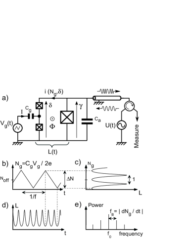
The quantronium device VionSc ; thesis is a split Cooper pair box that forms a loop including also a probe junction. The box island with total capacitance is defined by two small junctions having Josephson energies and , being an asymmetry coefficient. The superconducting phase of this island, conjugated to the number of extra Cooper pairs inside, forms the single degree of freedom of the box cercle . The third larger junction with critical current , in parallel with an added on-chip capacitor , forms a resonator with plasma frequency in the range zorin . Since this frequency is always smaller than the box transition frequency, we treat the phase difference across the probe junction as a classical variable. The same thus holds for the phase difference across the two box junctions in series, with the magnetic flux applied through the loop, and . The control parameters of the split-box are and the reduced gate charge , with the island gate capacitance, and the gate voltage. The Hamiltonian of the box writes
| (1) |
with .
The eigenenergies vary periodically with and (period ) thesis . The experiment consists in imposing a linear variation of the reduced quasi-momentum that induces a periodic evolution of the quantum state along the first Bloch band , at the Bloch frequency . Therefore, the current through the two small junctions, the associated effective inductance for small phase excursions
| (2) |
and hence the admittance as seen from the measuring line, vary periodically. We measure this admittance by microwave reflectometry, as for the RF-SET rfset . In our experiment, we apply a triangular modulation of the gate signal centered on , with peak to peak amplitude , and with frequency corresponding to . Due to the symmetry properties of the quantum states with respect to , the inductance varies as for a linear sweep, as shown in Fig. 1, provided that the extremal values of are integer or half-integer, with a Bloch frequency . In order to obtain the largest gate charge modulation of the inductance, the phase is adjusted at with the flux . When a small microwave signal at frequency is sent on the measuring line, the periodic modulation of the reflection factor yields sidebands in the spectrum of the reflected signal rfset , shifted from the carrier by multiples of , and called Bloch lines ms+s . Due to the periodic excitation, the stationary outgoing amplitude can be written as a series:
| (3) |
The circuit equations and the loop-current expression VionSc ; thesis allow to calculate all sideband amplitudes , which get smaller and become asymmetric when the sideband frequencies depart from the resonance.
The sample was fabricated using electron-beam lithography VionSc ; thesis and aluminum deposition and oxidation. In order to avoid quasiparticle poisoning, the island was made thinner than the leads (13 nm and 42 nm respectively), and gold quasiparticle traps were used sset . In the present experiment, a sizeable asymmetry was introduced on purpose in order to maintain a large gap at , which avoids microwave driven transitions towards excited bands. The sample was placed in a sample-holder fitted with microwave transmission lines, at a temperature The gate was connected to a -bandwidth RF line. The microwave signal, after reflecting on the probe junction, went through 3 circulators before being amplified by a cryogenic amplifier with noise temperature , and a room temperature amplifier. The signal was then either demodulated with the CW input signal, or sent to a spectrum analyzer. In the latter case, the applied power was , corresponding to phase excursions smaller than , and the total measurement gain was . As a function of and , the plasma resonance varied in the range , slightly below the circulator bandwidth, which yielded an extra attenuation of the signal due to a spurious interference with the leakage signal through circulator atten . Fitting the variations of the resonance yielded , , , and leading to .

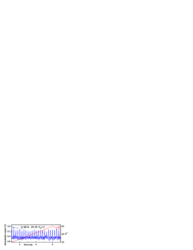
The reflected signal demodulated with the carrier is shown in Fig. 2 for a triangular gate voltage corresponding to . Due to noise, such time-domain measurements could only be performed within a 100 kHz bandwidth bandwidth . In the following, the reflectometry spectra are taken with a bandwidth resolution.
A series of spectra recorded at with , and taken with progressively tuned gate sweep signal amplitude and offset is shown in Fig. 3: when and are tuned as sketched in Fig. 1, the spectrum consists only of Bloch lines, as predicted, with linewidth limited by the spectrum analyzer.
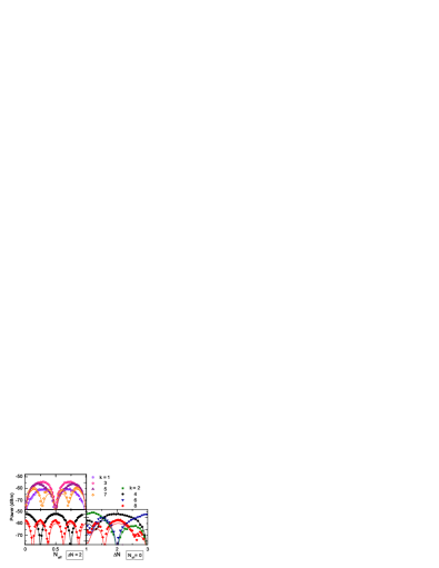
An example of comparison between the measured and predicted sideband amplitudes when or is varied is shown in Fig. 4 for . The measured amplitudes are well accounted for by the solution of Eq. 2, but for the carrier, which suffers from the spurious interference effect already mentioned atten . Although the overall agreement for the sidebands, and in particular the cancelation of some of them at particular offsets and amplitudes, demonstrate the phase-coherence of the measured signal, it does not prove that the quantronium undergoes a perfect coherent adiabatic evolution of its ground-state while and are varied: incoherent excitation/de-excitation processes are for instance not excluded. Because of the opposed inductance modulation in the excited state, they would only reduce the amplitude of the Bloch lines in proportion of the time spent in this state.
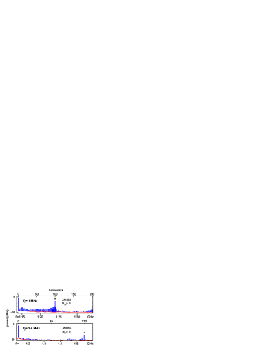
Spectra obtained at larger frequencies and larger amplitudes , corresponding respectively to currents and Bloch frequencies , , and , are shown in Fig. 5. These results demonstrate that Bloch oscillations persist at Bloch frequencies larger than the resonator bandwidth , even though Bloch lines become weaker. The successful current to frequency conversion performed up to currents using Bloch oscillations is the main result of this work. However, the amplitudes of the Bloch lines at these high frequencies are smaller than predicted by the model, and additional sidebands are present, which we attribute to the rounding of the gate triangular wave signal at its turning points, and to drifts of the gate-charge due to background charge noise. In principle, the theoretical maximum current is limited by two fundamental phenomena. First, the conversion mechanism requires , with to avoid multi-photon excitations. Second, the current must be low enough to avoid Zener transitions at where the gap is minimum. For the present experiment, the Zener probability , with the slope of away from , is negligible.
An important application of these experimental results could be to establish a direct link between a DC current and a frequency through the Bloch frequency in order to close the triangle of quantum metrology tri . Such an experiment would aim at measuring the current passing through a Quantum Hall bar device in terms of a rate of transferred Cooper pairs, in order to check the consistency of the Quantum Hall effect (QHE) with the AC Josephson effect. Using this latter effect, the Hall voltage across a QHE bar can indeed be related to a frequency through the relation . If the description of both QHE and Josephson experiments is exact, one predicts . A consistency check of this relation at the level is presently a major goal in metrology because, in conjunction with a metrological realization of the mass unit by a Watt-balance experiment bal , it would provide a serious basis for a redetermination of the SI unit system in terms of electrical experiments involving only fundamental constants. The large current , needed for QHE experiments, can be transposed to a smaller range using topologically defined transformers cccc . This current range, which is still beyond reach of single electron pumps pump or of direct electron counting experiments per , can be accessed with the sluice Cooper pair pump pekola , with Bloch oscillations in a single Josephson junction HavKuz , or with the method demonstrated here provided it can be used with a true DC current. In the last two cases, the impedance of the current source as seen from the single junction or from the box needs to be larger than to preserve single Cooper pair effects, and temporal fluctuations have to be small enough to obtain narrow Bloch lines enabling an accurate measurement of their frequency. Using for instance a resistive bias yields a Bloch linewidth of the order of the Bloch frequency HavKuz , due to thermal fluctuations of the self-heated bias resistor. Developing a suitable current source for charge injection is thus a challenging prerequisite to metrology experiments based on Bloch physics. High impedance dissipative linear Josephson arrays have already been used to demonstrate indirectly Bloch oscillations nose . Combining ohmic, inductive, and Josephson elements, and possibly non-equilibrium cooling techniques cool , might provide an adequate low-noise high impedance.
In conclusion, we have demonstrated the conversion of a current to a frequency in a Josephson device biased through a small capacitor, through the production of ultra narrow sidebands in the spectrum of a reflected microwave signal. This new method, which reaches a current range , would be extremely appealing for metrology if operated with a DC current.
We acknowledge discussions with M. Devoret, F. Piquemal, W. Poirier, N. Feltin, and within the Quantronics group. This work has been supported by the European project Eurosqip and by the C’nano grant ’signaux rapides’.
References
- (1) D.V. Averin, A.B. Zorin, and K.K. Likharev, Sov. Phys. JETP 61, 407 (1985); K.K. Likharev and A.B. Zorin, J. Low Temp. Phys. 59, 347 (1985).
- (2) F. Bloch, Z. Phys. 52, 555 (1928).
- (3) L.S. Kuzmin and D.B. Haviland, Phys. Rev. Lett. 67, 2890 (1991); L. Kuzmin et al., Physica B 203, 376 (1994).
- (4) S. Corlevi et al., Phys. Rev. Lett. 97, 096802 (2006).
- (5) M. Büttiker, Phys. Rev. B 36, 3548 (1987).
- (6) V. Bouchiat et al., Phys. Scr. T76, 165 (1998); Y. Nakamura, C.D. Chen, and J.S. Tsai, Phys. Rev. Lett. 79, 2328 (1997).
- (7) D. Vion et al., Science 296, 886 (2002); E. Collin et al., Phys. Rev. Lett. 93, 157005 (2004).
- (8) M.W. Keller, J.M. Martinis, and R.L. Kautz, Phys. Rev. Lett. 80, 4530 (1998); N.M. Zimmerman and M.W. Keller, Meas. Sci. Technol. 14, 1237 (2003).
- (9) J. J. Vartiainen et al., Appl. Phys. Lett. 90, 082102 (2007).
- (10) J. Bylander, T. Duty, and P. Delsing, Nature 434, 361 (2005).
- (11) A. Cottet, PhD thesis, Université Paris VI (2002), available at http://tel.ccsd.cnrs.fr (in English).
- (12) In contrast to the case of a current-biased junction, the phase is defined on a circle due to the quantization of .
- (13) A related setup was reported recently in J. Könemann et al., cond-mat/0701144.
- (14) R.J. Schoelkopf, Science, 280, 1238 (1998); A. Aassime et al., Appl. Phys. Lett. 79, 4031, (2001).
- (15) N. Boulant et al., International Symposium on Mesoscopic Superconductivity and Spintronics 2006 (MS+S2006), Takayanagi H., ed., World Scientific, Singapore (2006) [cond-mat/0605061].
- (16) O. Naaman and J. Aumentado, Phys. Rev. B 73, 172504 (2006); A. J. Ferguson et al., Phys. Rev. Lett. 97, 106603 (2006).
- (17) The circulator leakage requested to explain our data varied from to over the plasma frequency excursion range, which is compatible with room temperature measurements.
- (18) Note that a larger bandwidth was recently obtained in related electrometry setups sset .
- (19) M.W. Keller et al., Science 285, 1706 (1999); F. Piquemal and G. Geneves, Metrologia 37, 207 (2000); F. Delahaye and B. Jeckelmann, Metrologia 40, 217 (2003).
- (20) G. Geneves et al., IEEE Trans. Instr. Meas. 54, 850 (2005).
- (21) I. K. Harvey, Metrologia 12, 47 (1976).
- (22) O-P. Saira et al., Phys. Rev. Lett. 99, 027203 (2007), and refs. therein.