Electrically injected cavity polaritons
Abstract
We have realised a semiconductor quantum structure that produces electroluminescence while operating in the light-matter strong coupling regime. The mid-infrared light emitting device is composed of a quantum cascade structure embedded in a planar microcavity, based on the GaAs/AlGaAs material system. At zero bias, the structure is characterised using reflectivity measurements which show, up to room temperature, a wide polariton anticrossing between an intersubband transition and the resonant cavity photon mode. Under electrical injection the spectral features of the emitted light change drastically, as electrons are resonantly injected in a reduced part of the polariton branches. Our experiment demonstrates that electrons can be selectively injected into polariton states up to room temperature.
pacs:
73.21.fg, 73.40.Gk, 85.60.JbThe study of electron - hole excitations strongly coupled to photonic modes in a semiconductor micro-cavity, has motivated a wealth of fascinating experiments Weisbuch ; savvidis ; bose in the past ten years. Recently, the light - matter strong interaction has been observed also in a two-dimensional electron gas (2DEG) coupled to a cavity photon mode dini . These excitations, called intersubband (ISB) polaritons ciuti_PRB , have been experimentally demonstrated using angle-dependent reflectance spectroscopy of multiple 2DEGs anappara_APL2005 ; anappara_APL2006 . Recently, a photovoltaic probe of intersubband polaritons in a quantum cascade structure has also been realized sapienza .
The strong coupling regime may be especially interesting for light emitting devices (LED) based on ISB transitions. Their radiative efficiency is in fact very poor () because non-radiative phenomena control the lifetime of electrons in excited subbands (the radiative lifetime is ns in the mid-infrared while the non-radiative one is ps). In the strong-coupling regime, the light-matter interaction can be dominated by the time of a Rabi oscillation rather than the radiative lifetime, with a possible advantage in term of external efficiency. The possibility of a stimulated emission of ISB polaritons could also lead to inversionless mid and far infrared lasers, with lower thresholds with respect to quantum cascade lasers. In the context of light sources, devices based on electrical injection, rather than optical excitation, would be more suitable for applications.
Up to now, electrical injection of a micro-cavity LED in the strong coupling regime has only been reported in organic semiconductors nurmikko . Moreover, the description of a current injecting electrons into a polaritonic system constitutes a new physical framework that lacks a complete theoretical description. A first attempt to describe the coupling between an electronic reservoir and intersubband polaritons has been proposed in ref. ciuti_PRA . The authors derive an analytical expression for the electroluminescence by introducing the coupling of the polaritonic system with a bath of electronic excitations.
In the present paper, we report on the experimental realization of a GaAs/AlGaAs electroluminescent device working in the light-matter strong coupling regime. A quantum cascade (QC) structure is used as an active region, as proposed in ref. colombelli . Clear differences between electroluminescence (EL) and absorption spectra of the same structure are observed, thus pointing out the role of the electrical injection. A very good agreement between the experimental results and the simulations is found with a phenomenological model, in which the EL spectra are obtained as the product of the absorption spectra with a Gaussian filter function.
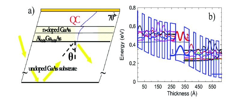
The sample (sketched in fig. 1a) is composed of a QC LED grown by molecular-beam epitaxy, on an undoped GaAs (001) substrate. The QC LED is placed within a metal/semiconductor planar micro-cavity, designed for the confinement of transverse magnetic polarized radiation. Light confinement is realized by sandwiching the QC structure between a bottom reflector made of a low refractive index Si-doped GaAs and Al0.95Ga0.05As layers and a top metallic mirror evaporated on the surface. The latter is also used as top electrical contact.
The band diagram of the QC LED, obtained with self-consistent Schrödinger-Poisson calculations, is presented in fig. 1b under an applied bias of 6 V. The radiative transition takes place in the largest well between the states labelled 1 and 2, whose nominal energy separation is meV. Electrical injection into the subband 2 is obtained by resonant tunnelling through an injection barrier sirtori_IEEE . Electrons are extracted from subband 1 through the states of a miniband, which also has the purpose to inject electrons into the following period. The injection region has been designed in order to have a tunnelling time out of the subband 1 longer than the scattering time from 2 to 1 in order to avoid population inversion and accumulate electrons into the subband 1. This is an essential feature for the observation of the strong coupling regime colombelli . Furthermore, the injection region has been highly doped ( cm-2, see caption of fig. 1) in order to provide a high density 2DEG in the well. As a consequence, the sample is also suitable for reflectivity measurements when no bias is applied nota_bd .
A photon confined within the micro-cavity can be absorbed promoting an electron to level 2, with the creation of an ISB excitation on top of the 2DEG. By varying the propagating angle of the light within the cavity, the energy of the photonic mode can be tuned across the energy of the ISB excitation. If the strong coupling regime is achieved, the degeneracy of the excitation and photonic states at resonance will be removed and the two branches will anticross. Angle resolved measurements will thus reveal the presence of intersubband polaritons in the system.
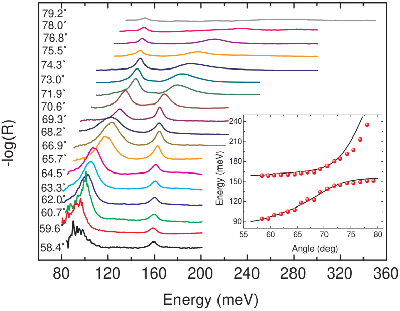
To this end, the sample has been prepared with polished facets (see fig. 1a) and a metallic layer [Ti(10 nm)/Au(500 nm)] was e-beam evaporated on the top surface, for standard reflectivity measurements liu . Angle resolved reflectivity spectra, performed at 78 K, are shown in fig. 2. Two peaks are clearly visible across a very wide angular range (almost the whole range where the cavity operates, between total internal reflection at and Brewster angle at ). In the inset of fig. 2 we have plotted the energy position of the two peaks (symbols) as a function of the internal angle in the cavity, showing an anticrossing feature at approximately footnote . We attribute the two branches in the inset of fig. 2 to the upper and lower polaritons (UP and LP respectively). It is worth mentioning that the strong coupling regime has also been observed in reflectivity up to 300 K with very similar features to those shown in fig. 2. In the inset of fig. 2 we have also plotted the LP and UP branches calculated in the transfer matrix formalism (line). In the simulations, the contribution of the ISB transition has been taken into account in the dielectric permittivity of the quantum well layers including an additional term in the form of an ensemble of classical polarized Lorentz oscillators, as in ref. dini . The dispersions of the Au ordal and of the doped layers Palik have also been included. In the calculations we used an electronic density in the fundamental subband cm-2 to reproduce the experimental results. This value is consistent with the results of Shubnikov-de Haas measurements which give 7.2 cm-2.
The energy splitting deduced from the inset of fig. 2 is 34 meV. It is worth noticing that this value is not the vacuum field Rabi splitting , which has to be deduced from the dispersion relation, where is the in-plane momentum of the photon. The relationship between and the light propagating angle inside the cavity reads: ciuti_PRB , where is the cavity refractive index and the energy of the considered excitation branch. This relationship introduces a strong distortion of the polariton branches, resulting in a value of the Rabi splitting meV.
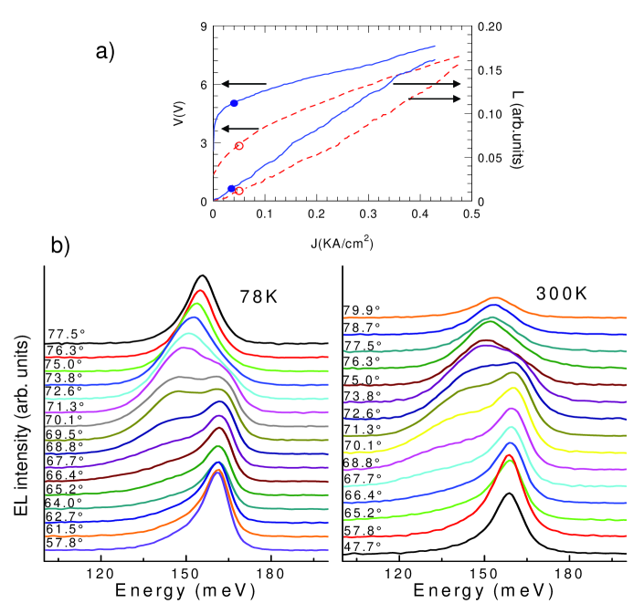
By applying an external bias to the device, the intersubband strong coupling regime can be investigated in emission, via EL measurements. The sample is thus mesa etched (circular 220 m diameter mesas), metallic contacts [Ni(10 nm)/Ge(60 nm)/Au(120 nm)/Ni(20 nm)/Au(200 nm)] are evaporated on top to allow current flow and the facet is polished with an angle of . The sample is soldered onto a copper holder, mounted onto the cold finger of a cryostat and the temperature is varied from 10 K to 300 K. The electrical and optical characteristics of the device at 78 K and 300 K are summarized in fig. 3a, where the evolution of the voltage and of the electroluminescence intensity as functions of the injected current density is shown. The structure presents a diode-like behavior, with an alignment at 5 V at 78 K. The output power shows a well defined linear dependence with the injected current. The EL spectra have been obtained by applying to the structure a voltage close to the alignment voltage (the working conditions for obtaining the spectra are shown by dots in fig. 3a), in order to keep the electronic density in the lowest subband as high as possible.
Fig. 3b presents the EL spectra measured at 78 K for an applied voltage of 5 V (left side) and at 300 K for an applied voltage of 2.8 V (right side) at different angles. The spectral features show a very strong angular dependence. For the angles close to we can observe at both temperatures two peaks, which are quite well separated in energy. On the contrary, when moving away from the resonance, only one peak is observed with a large shoulder.
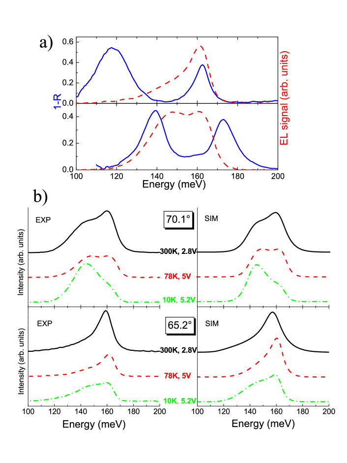
The EL spectra here presented are substantially different from the results obtained in reflectivity: it is important to underline that in reflectivity the polaritons are visible from about 90 to 240 meV, while in EL spectra the energy range where the experimental features are observable is approximately restricted within meV and meV. Furthermore, this energy interval (or ”energy window”) is different in the two sets of data shown in fig. 3 and depends on the voltage applied to the structure and on the temperature. In order to highlight this point, we show in fig. 4a a comparison between reflectivity and EL spectra measured at 78 K. In the top panel, the spectra at are presented. In reflectivity, we observe the UP and LP peaks, while the electroluminescence spectrum shows a single peak close to the energy of the upper polariton with a shoulder towards lower energies. In the lower panel, spectra at are presented: we observe the presence of two peaks in electroluminescence, with an energy difference of about 13 meV, a value much lower than the energy difference between the reflectivity peaks (34 meV).
The substantial difference between EL and reflectivity measurements originate from the coupling that the electronic component of the polariton states has with the injection region. In fact, for a fixed voltage, only one of the states of the injection region has a relevant probability to tunnel through the injection barrier, thus populating the polariton states. In order to simulate the EL spectra, we describe the injector as a Gaussian function , where is related to the energy position of the injector state with respect to the subband 1; reflects the broadening of the states in the injector due to disorder arising from interface and impurity scattering faist_APL . After simulating the absorption spectrum by using the transfer matrix formalism (obtained as , by neglecting the transmission through the upper mirror), we calculate the EL spectrum as the product between the Gaussian function and the absorption spectrum: . The parameters of the Gaussian function, and , are kept as fit parameters and determined by the comparison between the simulated and the measured EL spectra. We show in fig. 4b the measured (left side) and simulated (right side) electroluminescence, for three different temperatures (and voltages), at the same angles as in fig. 4a. We reproduce very well the shapes of the measured spectra in the entire angular range in the three temperature and voltage regimes. The energy position of has been fixed respectively to meV (10 K, 5.2 V), meV (78 K, 5 V), meV (300 K, 2.8 V). In the three cases, is close to the energy of the ISB transition ( meV at 10 K and 78 K, meV at 300 K). The reason for the differences in the values of is due to a different alignment of the states of the injector determined by the different applied bias. A good agreement with the experimental data is found with meV for 10 K and 78 K, and meV for 300 K. In the simulations, we used an electronic density reduced by a factor of 3 ( cm-2) as compared to the unbiased system; this value has been determined by a calculation of the electronic population as a function of the electric field applied to the structure aude and by a comparison between the simulated and measured electroluminescence spectra.
The phenomenological model described above can also be understood in the input-output theoretical framework developed in ref. ciuti_PRA . An analytical relationship between the EL and the absorption spectra may be found by exploiting the unitarity property of the input-output matrix ciuti_PRA to describe the coupling of the system with an electronic reservoir. In this formalism it can be shown that the EL spectrum takes the form: , where is the microcavity absorption spectrum and is related to the spectral properties of the electronic reservoir. This expression is analogue to the one used to interpret our experimental results footnote2 .
The very good agreement between the simulated and the measured spectra of fig. 4 is a strong proof of the observation of polaritonic luminescence, based on an electrical injection, up to room temperature. Furthermore, our experiment demonstrates that electrons can be selectively injected into polariton states.
In conclusion, we have realized a semiconductor EL device based on the light-matter strong coupling regime. The achievement of this regime has been demonstrated by reflectivity measurements, up to room temperature. Electroluminescence measurements show an electrical injection into polariton states up to room temperature. Our experimental results have been interpreted by using a phenomenological model, in which an energy filter related to the electrical injection is introduced. We believe that these results open the way to a new class of devices operating in the strong coupling regime. In the future, an optimized electronic resonant injection into the polariton branches could pave the way to the realization of an electrically pumped polariton laser.
Acknowledgements.
The authors thank I. Carusotto, H. C. Liu, I. Sagnes, N. Alayli, L. Largeau, O. Mauguin, S. De Liberato for fruitful discussions and help. The device fabrication has been performed at the nano-center Centrale Technologique Minerve at the Institut d’Electronique Fondamentale. We gratefully acknowledge support from EU MRTN-CT-2004-51240 POISE and ANR-05-NANO-049 INTERPOL.References
- (1) C. Weisbuch, M. Nishioka, A. Ishikawa, and Y. Arakawa, Phys. Rev. Lett. 69, 3314 (1992).
- (2) P. G. Savvidis, J. J. Baumberg, R. M. Stevenson, M. S. Skolnick, D. M. Whittaker and J. S. Roberts, Phys. Rev. Lett. 84, 1547 (2000).
- (3) J. Kasprzak, M. Richard, S. Kundermann, A. Baas, P. Jeambrun, J. M. J. Keeling, F. M. Marchetti, M. H. Szymanka, R. André, J. L. Staehli, V. Savona, P. B. Littlewood, B. Deveaud and Le Si Dang, Nature 443, 409 (2006).
- (4) D. Dini, R. Köhler, A. Tredicucci, G. Biasiol and L. Sorba, Phys. Rev. Lett. 90, 116401 (2003).
- (5) C. Ciuti, G. Bastard and I. Carusotto, Phys. Rev. B 72, 115303 (2005).
- (6) A. A. Anappara, A. Tredicucci, G. Biasiol and L. Sorba, Appl. Phys. Lett. 87, 051105 (2005).
- (7) A. A. Anappara, A. Tredicucci, F. Beltram, G. Biasiol and L. Sorba, Appl. Phys. Lett. 89, 171109 (2006).
- (8) L. Sapienza, A. Vasanelli, C. Ciuti, C. Manquest, C. Sirtori, R. Colombelli and U. Gennser, Appl. Phys. Lett. 90, 201101 (2007).
- (9) J. R. Tischler, M. S. Bradley, V. Bulovic, J. H. Song and A. Nurmikko, Phys. Rev. Lett. 95, 036401 (2005).
- (10) C. Ciuti and I. Carusotto, Phys. Rev. A 74, 033811 (2006).
- (11) R. Colombelli, C. Ciuti, Y. Chassagneux and C. Sirtori, Semicond. Sci. Technol. 20, 985 (2005).
- (12) C. Sirtori, F. Capasso, J. Faist, A. L. Hutchinson, D. L. Sivco and A. Y. Cho, IEEE Journal of Quantum Electronics 34, 1722 (1998).
- (13) For the band diagram at zero bias see ref. sapienza .
- (14) Intersubband Transitions in Quantum Wells: Physics and Device Applications I, edited by H.C.Liu and F.Capasso, Semiconductors and Semimetals vol.62, Academic Press, San Diego (2000).
- (15) The mixing of photonic and material excitation components is also evident from the behaviour of the linewidths as functions of the angle: the UP and LP show the same linewidth at resonance, when the two contributions are equally present in the polaritonic states.
- (16) M. A. Ordal, R. J. Bell, R. W. Alexander, L. L. Long and M. Querry, Appl. Optics 26, 744 (1987).
- (17) Handbook of Optical Constants of Solids, edited by E. D. Palik, Academic Press (1998).
- (18) J. Faist, F. Capasso, C. Sirtori, D. L. Sivco, A. L. Hutchinson, S. N. G. Chu, and A. Y. Cho, Appl. Phys. Lett. 65, 94 (1994).
- (19) A. Leuliet, private communication.
- (20) A more detailed theoretical description of the electrical injection into polaritonic states is beyond the scope of the present article and it is in progress.


