Magnetoresistance in an all-manganite heterostructure
Abstract
We study the magnetic and transport properties of all-manganite heterostructures consisting of ferromagnetic metallic electrodes separated by an antiferromagnetic barrier. We find that the magnetic ordering in the barrier is influenced by the relative orientation of the electrodes magnetization producing a large difference in resistance between the parallel and antiparallel orientations of the ferromagnetic layers. The external application of a magnetic field in a parallel configuration also leads to large magnetoresistance.
pacs:
75.47.Gk, 75.10.-b, 75.30.Kz, 75.50.EeHeterostructures of strongly correlated systems are currently in the spotlight due to the appearance of new electronic phases (electronic reconstruction) Okamoto and Millis (2004); Huijben et al. (2006); Lin et al. (2006); Kancharla and Dagotto (2006); Brey (2007) at interfaces between materials with strong electron-electron and electron-lattice interactions. Manganese perovskites are specially interesting because of their potential application in spintronics Zutic et al. (2004): in the ferromagnetic phase they are half-metals Pickett and Singh (1996); Park et al. (1998a) and, therefore, very efficient spin injectors and detectors Bowen et al. (2003); Yamada et al. (2004); Bibes and Barthélémy (2007). In bulk or thin films, manganites show an extremely large (colossal) magnetoresistance, and phase separation, fruit of the competition between very different phases ranging from metallic and ferromagnetic (FM) to insulating and antiferromagnetic (AF) Dagotto (2003); Israel et al. (2007). The different phases arise as a function of doping and composition. For instance, bulk La1-xSrxMnO3 (LSMO) is FM and metallic at the so-called optimal doping () with a above room temperature, while systems with smaller A-site cations, like bulk Pr1-xCaxMnO3 (PCMO), are AF (CE-type ordering van den Brink et al. (1999a)) and insulating (with charge/orbital order) at the same doping.
Manganite surfaces are known to behave differently from the bulk, the typical example being the striking suppression of the spin polarization of a free surface at temperatures much lower than the bulk ferromagnetic Park et al. (1998b); Calderón et al. (1999a). This could have a very negative effect on the tunneling magnetoresistance (TMR) Jullière (1975) of magnetic tunnel junctions consisting of half-metallic manganites separated by a thin insulating layer because TMR depends very strongly on the properties of the electrode/barrier interface LeClair et al. (2000). Indeed, early reports of TMR in manganite heterostructures showed a very strong decrease with increasing temperature Lu et al. (1996). TMR is defined as the difference in resistance between parallel (P) and antiparallel (AP) relative orientations of the magnetization in the ferromagnetic metallic electrodes [TMR]. Recently it has been found that interfaces of manganites with suitable materials are able to keep the spin polarization close to that of the bulk up to higher temperatures Yamada et al. (2004); Garcia et al. (2004); Ishii et al. (2006) with the concomitant enhancement of TMR. Traditionally, insulating barriers such as SrTiO3, LaAlO3, and NdGaO3 are used.
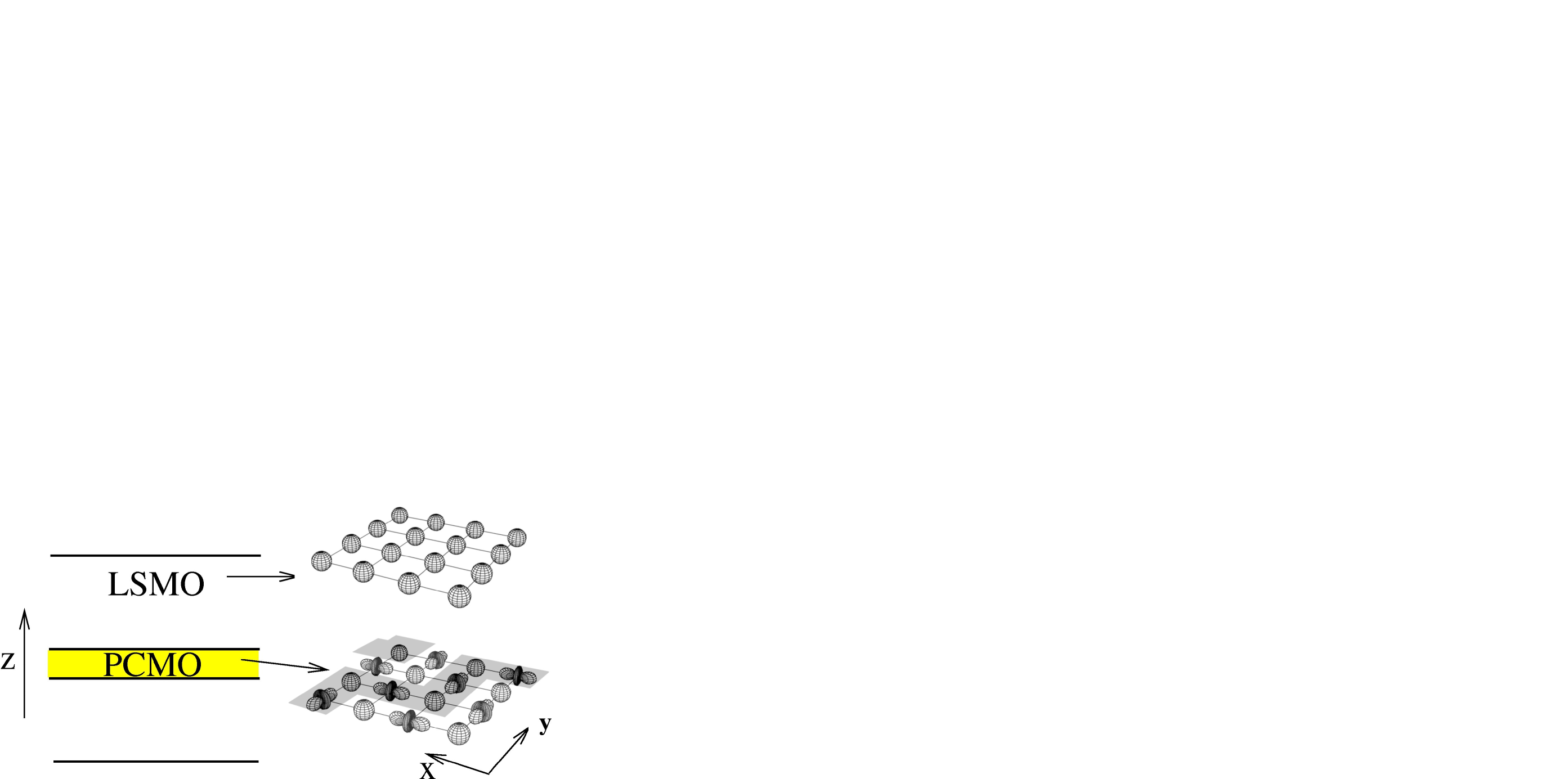
Here we focus on all-manganite heterostructures where the barriers are AF insulating manganites and study the effect of the FM layers on the ground state configuration at the barrier. These barriers are qualitatively different from other insulating barriers in that their electric and magnetic properties are expected to be influenced by the FM electrodes. In particular, we study the trilayer La2/3Sr1/3MnO3/Pr2/3Ca1/3MnO3/La2/3Sr1/3MnO3 illustrated in Fig. 1 Li et al. (2002); Niebieskikwiat et al. (2007). The LSMO layers are considered to have in-plane FM polarization (x-direction) in a P or AP configuration.
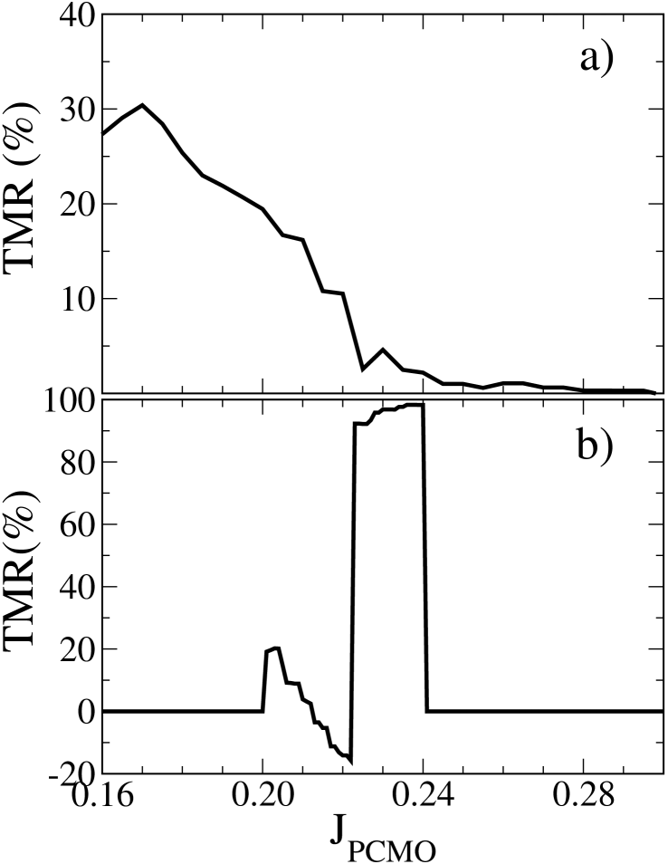
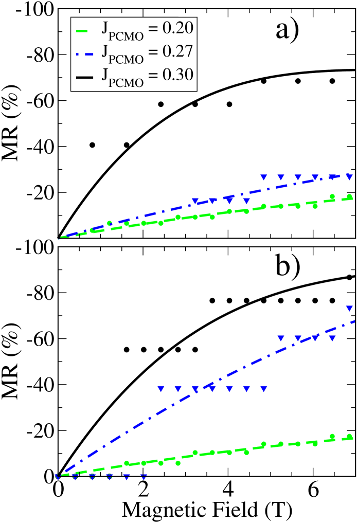
We find that the ground state configuration in the PCMO layer depends on the relative orientation of the magnetization in the LSMO layers and, as a consequence, the system shows a large TMR (see Fig. 2). In general terms, the P configuration induces FM ordering in the PCMO layer while the AP configuration tends to stabilize AF ordering in the barrier. The influence of the FM electrodes on the PCMO layer is due to a balance between the different coupling strengths in LSMO and PCMO and the charge transfer between the different layers. In principle, although the doping of divalent atoms is constant throughout the system, the strong electron-lattice interaction in the PCMO layer opens a gap in the density of states which produces a transfer of electrons towards the metallic FM areas. However, this charge transfer is limited by the long-ranged Coulomb interaction and, consequently, the PCMO layer can get more conductive and less AF than in the bulk foo . We also show that, in the P configuration, the application of a parallel magnetic field (along the x-direction) affects the PCMO layer magnetic ordering giving rise to negative MR (see Fig. 3).

We address these issues by finding the minimal energy spin, charge and orbital configuration in a very thin PCMO spacer [two (PCMO-2) to three (PCMO-3) lattice parameters, , wide] between two wider and perfectly ferromagnetic LSMO layers. The tight-binding Hamiltonian has the following termsBrey (2007):
| (1) | |||||
where creates an electron on the Mn i-site, in the orbital ( with and ). is the occupation number on the Mn i-site. The hopping amplitude depends on the Mn core spins orientation given by the angles and via (double-exchange mechanism), and on the orbitals involved where the superindices x,y, and z refer to the direction in the lattice. All the parameters are given in units of which is estimated to be eV. is an effective antiferromagnetic coupling between first neighbor Mn core spins which is different in the LSMO and PCMO layers (see below). is a repulsive interaction between electrons on a site lying on different orbitals, and is the long range Coulomb interaction between all the charges in the system, treated in the mean-field approximation
| (2) |
with the position of the Mn ions, the charge of the A-cation located at , and the dielectric constant of the material. The strength of the Coulomb interaction is given by the dimensionless parameter Lin et al. (2006).
The electron-lattice interaction has not been explicitely included in the Hamiltonian (1). However, the effect of this coupling on the ground state energies can be described using an effective van den Brink et al. (1999b). In particular, the ground state of Hamiltonian (1) for a bulk system with is the CE-type AF ordering associated to the lattice distortions that produce the charge and orbital ordering illustrated in Fig. 1. The values for that effectively include the electron-lattice coupling are therefore larger than the ones inferred from the magnetic ordering only ( from superexchange between the electrons is meV) Dagotto (2003). The FM layers (LSMO) are well described by small values of (for simplicity, we consider ), while for the barrier (PCMO) we use . Reasonable values for the other two parameters are and Brey (2007). The results presented below are qualitatively insensitive to moderate changes of these two parameters. The Hamiltonian is solved self-consistently in heterostructures consisting of a thin PCMO layer and two wide LSMO FM layers (wide enough to reproduce bulk behavior).
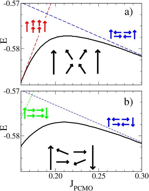
In Fig. 4 we show the total energy versus for a pure FM, CE and an intermediate canted configuration of the PCMO-2 layer for P and AP configurations of the electrodes. All the other magnetic orderings considered were higher in energy in this range of parameters. For , the magnetic ground state configuration in the spacer is always canted with the canting angle depending on the value of and on the relative orientation of the magnetization in the LSMO layers. In the P configuration [Fig. 4(a)], PCMO tends to order more FM and collinearly with the electrodes, while for the AP case [Fig. 4(b)], the PCMO configuration corresponds to smaller magnetization and the spins lie perpendicular to the electrodes magnetization. The results for PCMO-3 (not shown) are qualitatively similar.


For PCMO-2 and relatively small (), the magnetic order at the barrier is canted, and the charge/orbital order is mostly suppressed due to charge transfer between the layers. FM correlations and, due to double exchange, conductance are larger in the P configuration than in the AP configuration. Therefore, this geometry could be used as a magnetic sensor. The conductance has been calculated numerically via Kubo formula Vergés (1999); Calderón et al. (1999b) for a trilayer with semi-infinite FM LSMO leads. The results for a PCMO-2 spacer are plotted in Fig. 2 (a) where a finite TMR for is shown. The superstructure in the curve is due to numerical inaccuracies except for the peak at , which is quite robust (the TMR increases monotonically in the range ). This peak appears because, below , the P ground state configuration is almost FM [Fig. 4 (a)] while the AP configuration is already canted [Fig. 4 (b)] and, as a consequence, increases faster with than .
For PCMO-3 there is a range of parameters, , for which the TMR is close to its maximum possible value of . In this range, the P configuration is metallic as it has a relatively large FM component in the three Mn planes that constitute the barrier, while the AP configuration is insulating and corresponds to perfect CE in the middle atomic plane and canted FM in the outer planes. For smaller values of (), for both the P and AP configurations, the middle plane is a perfect CE while the outer planes are essentially FM and parallel to the nearest electrode; this leads to and, hence, TMR. The negative TMR at is produced by the different dependence of the canting angle on for P and AP configurations. The different behavior of the TMR in PCMO-2 and PCMO-3 is due to the limited charge transfer in the middle Mn plane of the wider barrier.
For large (), see Figs. 2 (a) and (b), or wider PCMO spacers (PCMO-n with ), the AF ordering in the barrier is preserved and the system does not show TMR at all: both and are strictly .
We have also calculated the MR in the P configuration that results of applying an external magnetic field parallel to the magnetization in the electrodes. The results are shown for PCMO-2 and PCMO-3 in Fig. 3. We define MR so its maximum possible absolute value is MR. The dots represent the numerical values and the steps are an artifice of the calculation that considers a discrete set of values of the canting angle. The lines are a fit to the data. When a magnetic field is applied, the system is effectively moving towards smaller values of (see Fig. 4) and therefore towards less resistive configurations, hence the negative MR. This MR is produced by the alignment of the barrier spins with the applied field and is smaller than the CMR measured in bulk PCMO Anane et al. (1999) which is probably related to inhomogeneities and phase separation. The real advantage of this heterostructure as a magnetic sensor is that its resistivity can be orders of magnitude smaller than the bulk PCMO’s (mainly because there is no gap at the Fermi energy for the thin spacers in the P configuration). As a guideline, the resistivity of bulk LSMO at low is cm Urushibara et al. (1995), much smaller than that of bulk PCMO cm (cm at T) Yoshizawa et al. (1996).
It is well known that strain (produced by lattice mismatch between the substrate and the thin films) can affect the orbital ordering Tokura and Nagaosa (2000). In the studied heterostructure with an STO substrate Niebieskikwiat et al. (2007) the in-plane lattice parameter is for all layers while the out-of-plane lattice parameters are (LSMO) and (PCMO), slightly smaller (less than a in any case) than the bulk values. Our calculations are done in a cubic lattice but the variations in unit cell dimensions in actual heterostructures Niebieskikwiat et al. (2007) are not expected to produce a dramatical change in the orbital ordering Tokura and Nagaosa (2000). In any case it would emphasize the tendency to CE ordering in the PCMO barrier that can be included in our model simply by increasing the value of . Strain can also produce phase separation Infante et al. (2007) and colossal magnetoresistance Ahn et al. (2004). The inclusion of phase separation in our model would lead to an increase of both TMR (Fig. 2) and MR (Fig. 3) with respect to the calculated values.
In conclusion, we have studied the electric and magnetic properties of an all-manganite heterostructure with homogeneous doping of divalent cations. The system consists of two FM and metallic electrodes (La2/3Sr1/3MnO3) and a thin AF barrier (Pr2/3Ca1/3MnO3). We show that the ground state configuration in the PCMO layer depends on the relative orientation of the FM electrodes (parallel or antiparallel) rendering these heterostructures useful as magnetic sensors. Underlying this result is the fact that charge transfer between the layers with different coupling strengths alters the electric and magnetic properties of the thin PCMO layer (which is AF and insulating in bulk) increasing its magnetization and conductivity. Therefore, the resulting heterostructures have low resistivity in a wide range of parameters, mainly in the parallel configuration, at which an external field applied can produce a large negative MR.
We thank J.A. Vergés for fruitful discussions. This work is supported by MAT2006-03741 (MEC, Spain). M.J.C. also acknowledges Programa Ramón y Cajal (MEC, Spain).
References
- Okamoto and Millis (2004) S. Okamoto and A. Millis, Nature 428, 630 (2004).
- Huijben et al. (2006) M. Huijben, G. Rijnders, D. H. A. Blank, S. Bals, S. V. Aert, J. Verbeeck, G. V. Tendeloo, A. Brinkman, and H. Hilgenkamp, Nature Materials 5, 556 (2006).
- Lin et al. (2006) C. Lin, S. Okamoto, and A. J. Millis, Phys. Rev. B 73, 041104 (2006).
- Kancharla and Dagotto (2006) S. S. Kancharla and E. Dagotto, Phys. Rev. B 74, 195427 (2006).
- Brey (2007) L. Brey, Phys. Rev. B 75, 104423 (2007).
- Zutic et al. (2004) I. Zutic, J. Fabian, and S. Das Sarma, Rev. Mod. Phys. 76, 323 (2004).
- Pickett and Singh (1996) W. E. Pickett and D. Singh, Phys. Rev. B 53, 1146 (1996).
- Park et al. (1998a) J.-H. Park, E. Vescovo, H.-J. Kim, C. Kwon, R. Ramesh, and T. Venkatesan, Nature (London) 392, 794 (1998a).
- Bowen et al. (2003) M. Bowen, M. Bibes, A. Barthelemy, J.-P. Contour, A. Anane, Y. Lemaitre, and A. Fert, Appl. Phys. Lett. 82, 233 (2003).
- Yamada et al. (2004) H. Yamada, Y. Ogawa, Y. Ishii, H. Sato, M. Kawasaki, H. Akoh, and Y. Tokura, Science 305, 646 (2004).
- Bibes and Barthélémy (2007) M. Bibes and A. Barthélémy, IEEE Trans. Electron. Devices 54, 1003 (2007).
- Dagotto (2003) E. Dagotto, Nanoscale Phase Separation and Colossal Magnetoresistance (Springer-Verlag, Berlin, 2003).
- Israel et al. (2007) C. Israel, M. J. Calderón, and N. D. Mathur, Materials Today 10, 24 (2007).
- van den Brink et al. (1999a) J. van den Brink, G. Khaliullin, and D. Khomskii, Phys. Rev. Lett. 83, 5118 (1999a).
- Park et al. (1998b) J.-H. Park, E. Vescovo, H.-J. Kim, C. Kwon, R. Ramesh, and T.Venkatesan, Phys. Rev. Lett. 81, 1953 (1998b).
- Calderón et al. (1999a) M. J. Calderón, L. Brey, and F. Guinea, Phys. Rev. B 60, 6698 (1999a).
- Jullière (1975) M. Jullière, Phys. Lett. 54A, 225 (1975).
- LeClair et al. (2000) P. LeClair, H. J. M. Swagten, J. T. Kohlhepp, R. J. M. van de Veerdonk, and W. J. M. de Jonge, Phys. Rev. Lett. 84, 2933 (2000).
- Lu et al. (1996) Y. Lu, X. W. Li, G. Q. Gong, G. Xiao, A. Gupta, P. Lecoeur, J. Z. Sun, Y. Y. Wang, and V. P. Dravid, Phys. Rev. B 54, R8357 (1996).
- Garcia et al. (2004) V. Garcia, M. Bibes, A. Barthelemy, M. Bowen, E. Jacquet, J.-P. Contour, and A. Fert, Phys. Rev. B 69, 052403 (2004).
- Ishii et al. (2006) Y. Ishii, H. Yamada, H. Sato, H. Akoh, Y. Ogawa, M. Kawasaki, and Y. Tokura, Appl. Phys. Lett. 89, 042509 (2006).
- Li et al. (2002) H. Li, J. R. Sun, and H. K. Wong, Appl. Phys. Lett. 80, 628 (2002).
- Niebieskikwiat et al. (2007) D. Niebieskikwiat, M. B. Salomon, L. E. Hueso, N. D. Mathur, and J. A. Borchers (2007), cond-mat/0702350.
- (24) Note that PCMO at is insulating because there is a gap at the Fermi energy, while for , which is the case here, PCMO is insulating when AF ordering produces no extended states at the Fermi energy.
- van den Brink et al. (1999b) J. van den Brink, G. Khaliullin, and D. Khomskii, Phys. Rev. Lett. 83, 5118 (1999b).
- Calderón et al. (1999b) M. J. Calderón, J. A. Vergés, and L. Brey, Phys. Rev. B 59, 4170 (1999b).
- Vergés (1999) J. Vergés, Comp. Phys. Comm. 118, 71 (1999).
- Anane et al. (1999) A. Anane, J.-P. Renard, L. Reversat, C. Dupas, P. Veillet, M. Viret, L. Pinsard, and A. Revcolevschi, Phys. Rev. B 59, 77 (1999).
- Urushibara et al. (1995) A. Urushibara, Y. Moritomo, T. Arima, A. Asamitsu, G. Kido, and Y. Tokura, Phys. Rev. B 51, 14103 (1995).
- Yoshizawa et al. (1996) H. Yoshizawa, H. Kawano, Y. Tomioka, and Y. Tokura, J. Phys. Soc. Jpn. 65, 1043 (1996).
- Tokura and Nagaosa (2000) Y. Tokura and N. Nagaosa, Science 288, 462 (2000).
- Infante et al. (2007) I. Infante, S. Estradé, F. Sánchez, J. Arbiol, F. Peiró, V. Laukhin, J. P. Espinós, M. Wojcik, E. Jedryka, and J. Fontcuberta (2007), arXiv:0708.3602.
- Ahn et al. (2004) K. Ahn, T. Lookman, and A. Bishop, Nature 428, 401 (2004).