SiPM development for Astroparticle Physics applications
Abstract
The SiPM is a novel solid state photodetector which can be operated in the single photon counting mode. It has excellent features, such as high quantum efficiency, good charge resolution, fast response, very compact size, high gain of , very low power consumption, immunity to the magnetic field and low bias voltage (30-70V). Drawbacks of this device currently are a large dark current, crosstalk between micropixels and relatively low sensitivity to UV and blue light. In the last few years, we have developed large size SiPMs ( mm2 and mm2) for applications in the imaging atmospheric Cherenkov telescopes, MAGIC and CTA, and in the space-borne fluorescence telescope EUSO. The current status of the SiPM development by MPI and MEPhI will be presented.
1 Introduction
In Astroparticle Physics experiments, we measure the rare and low flux events, and naturally the instrument will become large in area and volume. Photodetection techniques play an important role in the detection of these rare and low flux events. We require low level light (LLL) detectors working in single photon counting mode. We record the time profile of signals or require the very fast timing of signals. The imaging of the signal plays a very important role in Imaging Air Cherenkov Telescopes (IACTs) for high energy gamma rays and in the air fluorescence technique for Ultra High Energy Cosmic Rays (UHECRs).
The SiPM is a solid state photodetector developed for applications in High Energy Physics, Astroparticle Physics and Medical Science. For Astroparticle Physics applications, the most attractive feature of the SiPM is its high photodetection efficiency () and the capability of single photon counting. Further, there are many other advantages, such as the compactness of its size and volume, the low bias voltages, the very high gain of , the low power consumption, etc.. At present, the major problems of SiPMs are the small size, the cross talk between micropixels in the SiPM and the high dark current.
For the MAGIC telescope [1], the high photodetection efficiency will allow us to lower the threshold energy of gamma ray detection down to 10-20 GeV. We can also design new smaller and inexpensive Cherenkov telescopes keeping the performance at an equally high level. This allows us to consider an array of smaller high performance telescopes at a low budget. For MAGIC, the pixel size of the photodetector shall be a mm size (corresponding to with a winston cone). Even if we consider smaller pixels below , we do not gain in angular resolution and gamma/hadron separation.
For the space-borne air fluorescence detector EUSO[3], photodetectors with a size of mm are required for pixel imaging. The high photodetection efficiency will ensure the detection of UHECRs above eV and allow a large overlap in the energy range with ground based detectors, Auger[4] and TA[5]. Alternatively it will allow us to use the high altitude orbit or tilted mode to cover larger detection volumes for UHECRs. Characteristics like the low power consumption and insensitivity to magnetic fields are important advantages for space detectors.
Therefore, the larger size SiPM of mm2 or even mm2, with high photondetecion efficiency, low dark rate, low crosstalk and enhanced sensitivity in UV and blue light is the prime target of our SiPM development. Silicon itself has the nice feature of nearly internal quantum efficiency. The increase of the filling factor of the sensitive area on the device surface and the increase of the Geiger efficiency will give us a very high photodetection efficiency.
2 Structure and operation of the SiPM
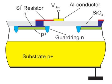
The SiPM consists of an array of a large number of micropixels (avalanche diodes) working in Geiger mode. The schematic picture of the individual micropixel’s structure is shown in figure 1. This micropixel works somehow in digital mode, giving us the signal in each Geiger discharge. Here, is the capacitance between anode and cathode of the avalanche diode, is the breakdown voltage of micropixel (avalanche diode), is called over voltage. The typical is . The anodes of all micropixels are joined together on a common substrate and are working on common load in case of n on p structure.
The operation of the individual micropixel is as follows. The micropixel is biased with a higher voltage than the breakdown voltage. This over voltage is typically or of the breakdown voltage. The micropixel is then kept in a meta-stable condition, and if a pair of electron and hole is created in the depletion or drift region by an incident photon, a Geiger discharge will be triggered. The current flow from the biasing circuit through the quenching register causes the bias voltage to drop and the Geiger process will stop automatically. The biasing circuit will recharge the capacitance of the SiPM to raise the bias voltage again up to the meta-stable over voltage. This recharge takes typically sec. The dark rate (night sky back ground, or dark current) DR per micropixel of m2 or m2 is usually low enough, i.e. kHz, even at room temperature, so the dead time and the decrease of photodetection efficiency can be negligibly small.
3 Development of SiPMs for MAGIC, CTA and EUSO
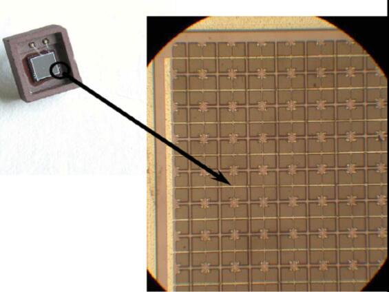
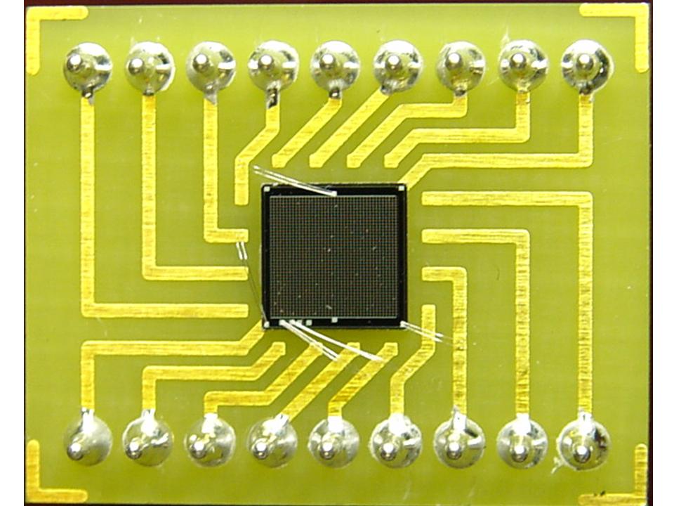
MPI and MEPhI have developed SiPMs with a size of mm2 and mm2 for MAGIC [1], CTA [2] and EUSO [3] applications as shown in figure 2 and figure 3[6,7,8,9]. The micropixel size is enlarged to m2 to get a higher filling factor of the sensitive region, in case of the mm2 SiPM. The devices were manufactured by the company Pulsar in Moscow.
3.1 Dark Rate
The dark rate of SiPMs is about MHz/mm2 at room temperature (). Dark current is produced by two mechanisms, i.e. the electric field assisted tunneling effect and the thermal effect. The dark current can be reduced by one or two orders of magnitude by cooling the temperature down to or in our devices, respectively. In our device the main component of dark current is the thermal one. The clever design avoids unnecessary extremely high electric fields will reduce the electric field assisted tunneling. The usage of ultra pure silicon wafers, the reduction of the volume of depletion and drift regions will help to reduce the dark rate.
3.2 Optical Crosstalk
The Optical Crosstalk (OC) is a specific phenomenon in SiPMs. The Geiger avalanche in one micropixel will provoke the emission of light, typically photons/avalanche of , and these photons will hit other pixels. This means that the single ph.e. has a chance to produce a multiple ph.e. signal. The emission of light is proportional to the Geiger gain. The Geiger efficiency which determines the final photodetection efficiency has also a strong positive dependence on the Geiger gain. Therefore, if we want to obtain a high photodetection efficiency, we need to operate SiPMs in high Geiger gain. This condition will introduce severe optical crosstalk in SiPMs. To avoid this problem we have introduced the OC suppression structure.
Optical crosstalk entails a serious problem in our specific usage, because we use photodetectors not only to record photon intensity but also to trigger events. Especially in the Cherenkov experiment and air fluorescence experiment, we have a high rate of background photons from the night sky. Even if there are a series of single ph.e., this optical crosstalk produces multiple ph.e. signals with a high rate and we are consequently required to effectively set the trigger threshold high in order to obtain a reasonable trigger rate.
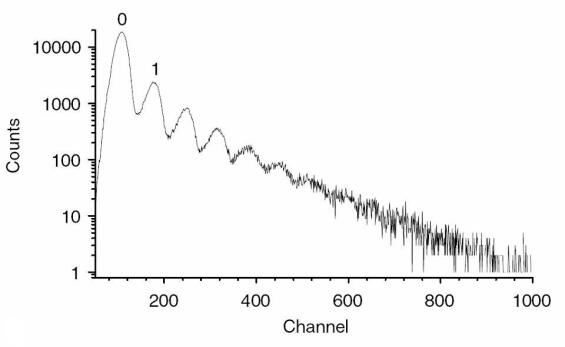
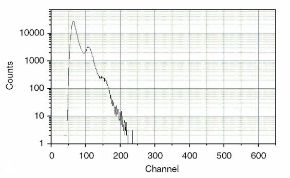
The top panel of figure 4 shows the pulse height distribution of dark rate in the standard SiPM without the OC suppression structure. We can see the exponential long tail in the multiple ph.e. region. These large pulses will raise the trigger threshold like after pulses in PMTs. By manufacturing the OC suppression structure (the groove structures between micropixels which block the transmission of light between micropixels through silicon), we succeed to suppress these unfavorable optical crosstalk. As shown in the bottom of figure 4, the optical crosstalk level was significantly reduced by this improvement. We can evaluate this improvement with the parameter of the Excess Noise Factor (ENF); the ENF of about 1.6 was improved to with the OC suppression structure.
3.3 Photodetection efficiency
Photodetection efficiency PDE is determined by four factors, i.e. the light transmission from surface to depletion or drift layers , the filling factor of the sensitive area, (sensitive area)/(all area) , the quantum efficiency of silicon , and the Geiger efficiency .
Silicon has a high reflectivity index , and with AR coating we can increase the light transmission up to a level. As shown in figure 1, there are guard rings, quenching registers, aluminum conductors for bias voltage supply around micropixels. This structure will limit the filling factor to . The internal quantum efficiency of silicon is close to , and the Geiger efficiency can be raised up to in high gain operation (high over voltage). Theoretically, the total PDE can be increased up to with the existing technologies.
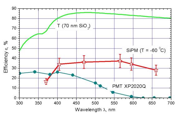
The PDE of a mm2 SiPM is about between 450nm and 550nm[6]. This mm2 SiPM consists of micropixels with a size of m2 (filling factor of ).
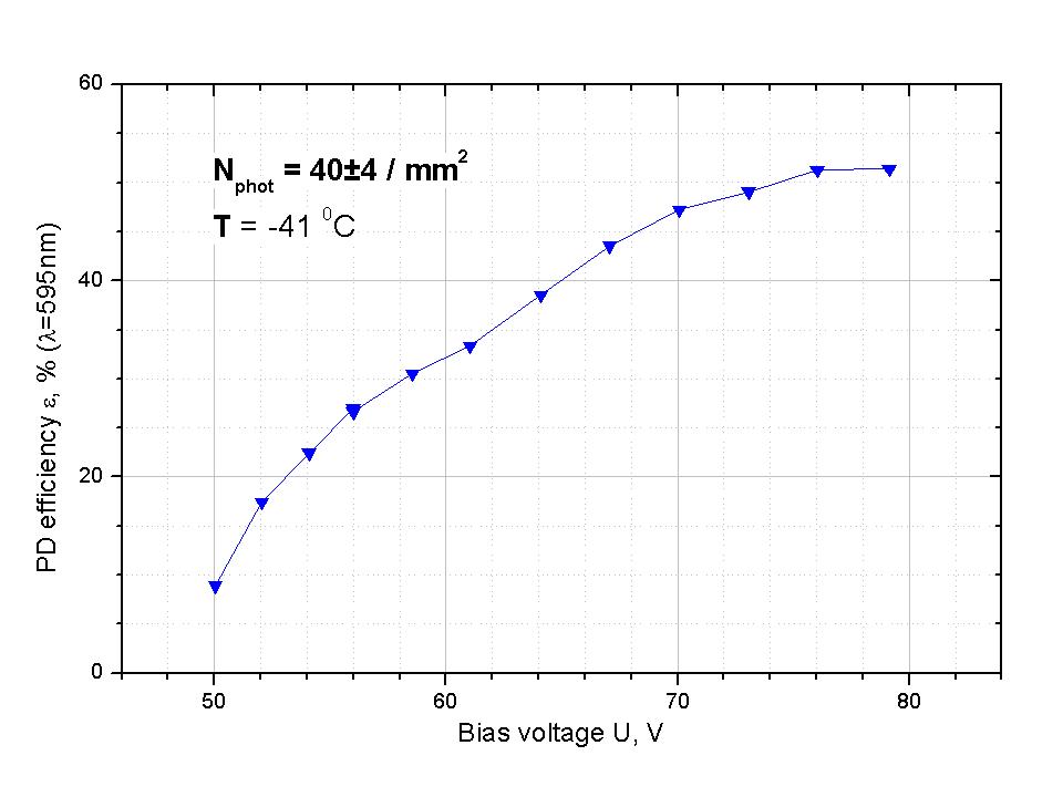
The SiPM of of mm2 consists of 1600 (40x40) micropixels with the size of m2 (the filling factor of ). The PDE of such a structure is shown in figure 5. For large overvoltages where the Geiger efficiency is close to , the PDE of a m2 structure reaches as shown in figure 6.
Conclusion
We have successfully developed mm2 and mm2 SiPMs. Their characteristics are almost satisfactory, but we consider further developments/improvements, the enhancement of UV-Blue light sensitivity with reverse structure (p on n), and larger SiPMs of mm2 size or the array of SiPMs of mm2 size for MAGIC [1], CTA [2] and EUSO [3] applications.
Acknowledgements
We would like to acknowledge the support by Max-Planck-Society.
Reference
[1] http://wwwmagic.mppmu.mpg.de/
[2] see contributions in this conference
[3] http://euso.riken.go.jp/
[4] http://www.auger.org/
[5] http://www-ta.icrr.u-tokyo.ac.jp/
[6] B. Dolgoshein et al., NIM A563 (2006) 368.
[7] R. Mirzoyan et al., N.I.M. A572 (2007) 493.
[8] P. Buzhan et al., N.I.M. A567 (2006) 78.
[9] A.N. Otte et al., N.I.M. A 545 (2005) 705.