Monovacancy and Substitutional Defects in Hexagonal Silicon Nanotubes
Abstract
We present a first-principle study of geometrical and electronic structure of hexagonal single-walled silicon nanotubes with a monovacancy or a substitutional defect. The C, Al or P atoms are chosen as substitutional impurities. It is found that the defect such as a monovacancy or a substitutional impurity results in deformation of the hexagonal single-walled silicon nanotube. In both cases, a relatively localized unoccupied state near the Fermi level occurs due to this local deformation. The difference in geometrical and electronic properties of different substitutional impurities is discussed.
pacs:
73.50.-h; 73.20.Hb; 73.20.AtCubic-diamond bulk silicon is a very well-known semiconducting material with an energy band gap of 1.2 eV. Unlike the cubic-diamond silicon, it would be hard to form one-dimensional single-walled silicon nanotubes (SiNTs) mainly because silicon prefers bonds to bonds. However, Bai and his co-workersBai suggested Si tubes formed by the top-to-top stacking of square, pentagonal and hexagonal silicon structures and showed using ab initio calculations that the pentagonal and hexagonal SiNTs may be locally stable in vacuum and be metallic. Thus, their work provided computational evidences for a possible existence of such one-dimensional silicon nanostructures, although those structures have not been observed experimentally yet. Therefore, at this point, it is very valuable to theoretically investigate the stability and related electronic structure of these silicon nanostructures with some defects.
In this Letter, we report the modification in geometrical and electronic structure of hexagonal single-walled silicon nanotubes with a monovacancy or a substitutional defect. The first-principles pseudopotential calculations are carried out based on the density functional theoryKohn-Sham within the generalized gradient approximation for the exchange-correlation functional. The ionic potential is described with the Vanderbilt-type ultrasoft pseudopotential.Vanderbilt Wave functions are expanded in a plane wave basis set with an energy cutoff of 21 Ry implemented in the PWSCF code.pwscf As a model system, we choose the hexagonal SiNT with a monovacancy or a substitutional defect. The C, Al or P atoms are chosen as substitutional impurities. All chosen model systems are treated by a supercell with the periodic boundary condition. The supercell in the lateral direction is as large as 19.2 Å and it has 16 times the minimal unit cell (16 2.4 Å) in the tube axis direction. The structures are relaxed until the Hellmann-Feynman forces are smaller than 0.05 eV/Å. The Brillouin-zone integration is done within the Monkhorst-Pack schemeMP using k-point sampling. To understand the features of charge distribution of our models, we perform the Mulliken population analysis using a numerical atomic orbital basis set in the OpenMX codeOzaki1 ; Ozaki2 with a kinetic energy cutoff of 150 Ry. For this Mulliken population analysis, norm-conserving Kleinman-Bylander pseudopotentialsTroullier ; Kleinman are employed.
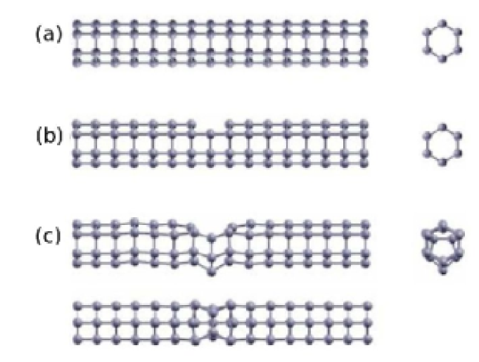
First, we calculate hexagonal SiNTs with or without a monovacancy shown in Fig. 1. If a single Si atom is removed from the nanotube, two of four Si atoms around the vacancy rebond (bond length of 2.42 Å) to form a pentagonal cross section. In the case of cubic-diamond bulk silicon, the lattice constant is 5.43 Å, which corresponds to the Si-Si bond length of 2.35 Å. Note that a buckled honeycomb planar structureDurgun of silicon has the average Si-Si bond length of 2.2 Å. The rebonded two atoms are perpendicular to the tube axis. Although other two Si atoms have dangling bonds even after the relaxation, their dangling bond characters become weak since the two Si atoms make strong bonds with three adjacent Si atoms (bond length of 2.322.36 Å). The formation energy () of a single vacancy in an SiNT is 16.3 eV (4.07 eV per bond). In the optimized structure, the Si atom on the opposite side to the monovacancy is protruded by 1 Å from the surface of the nanotube. The bonding angle with respect to this protruded Si atom at the pentagonal defect is 89.6∘ as shown in Fig. 1(c). Molecular dynamics (MD) simulations revealed that pentagonal and hexagonal SiNTs can remain stable.Bai ; Durgun Our MD simulation result shows that the SiNT is somewhat distorted but not broken when a monovacancy is formed at 600 K.
Such locally large distortion may affect the band structure and charge distribution of the SiNT. In terms of the Mulliken population analysis, we find an interesting feature. The protruded Si atom on the opposite side to the vacancy obtains 0.12 and its adjacent Si atoms lose electrons: Each of two adjacent Si atoms in the tube axis direction loses 0.025 , while each of two in the circumference direction loses 0.035 . On the other hand, the two rebonded Si atoms lose 0.073 , respectively.
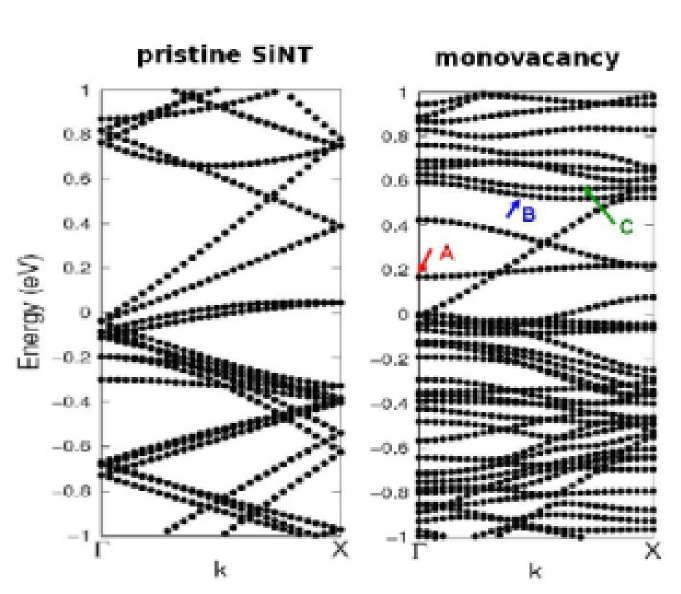
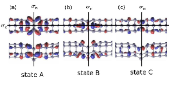
As mentioned above, Fig. 2(a) clearly shows that the hexagonal SiNT has the metallic character.Bai When a monovacancy is formed in the SiNT, the energy band structure is changed accordingly. There are prominent localized states above the Fermi level. Especially, a localized state (state A) originating from the structure distortion gives a flat band around 0.2 eV above the Fermi level as denoted by a downward arrow in Fig. 2(b). The isodensity surface plot of this unoccupied localized state (ULS) is presented in Fig. 3(a). In addition, a pentagon as a topological defect also gives rise to two ULSs (states B and C) near +0.6 eV as depicted by upward arrows in Fig. 2(b). Interestingly, Figs. 3(b) and (c) show that the localized states by a pentagonal defect are split into even and odd parity states with respect to the mirror planes ( and ) containing and normal to the nanotube axis, respectively.
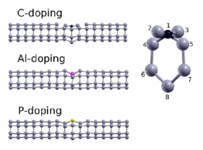
Next, we present the geometrical and electronic structure of a hexagonal SiNT with a carbon, aluminum or phosphorus as a substitutional impurity, shown in Fig. 4. In the case of the C doping, the C-Si bond length (C1-Si2 and C1-Si3) parallel to the tube axis is 1.93 Å and that (C1-Si4 and C1-Si5) perpendicular to the axis is 1.92 Å. The C atom is buckled inward by 0.4 Å and the Si8 atom on the opposite side to the C dopant is protruded outward by 0.6 Å. Owing to the strain effect, Si-Si bond breaking occurs near the defect site. The bond angle between C and adjacent Si atoms, Si2C1Si3, parallel to the tube axis are 165.8∘ and Si4C1Si5 perpendicular to the axis is 120.6∘. For the Al doping, the Al-Si bond lengths parallel and perpendicular to the tube axis are 2.58 and 2.61 Å, respectively. Here the Al atom is buckled inward by 0.7 Å and the Si atom on the opposite side to the Al dopant is buckled inward by 0.1 Å. The bond angle between Al and adjacent Si atoms parallel to the tube axis are 133.1∘ and that perpendicular to the axis is 140.3∘. In contrast, the P dopant shows an outward buckling by 0.3 Å. Such a trend is shown for boron nitride nanotubes,Rubio where nitrogen atoms are buckled outward and boron atoms are inward, which is associated with unpaired electrons. For the P doping, the Si atom on the opposite side to the P dopant is buckled outward by 0.3 Å. The P-Si bond lengths parallel and perpendicular to the tube axis are 2.50 and 2.30 Å, respectively. The bond angle between P and adjacent Si atoms parallel to the tube axis are 145.5∘ and that perpendicular to the axis is 102.3∘. Each impurity (C, Al or P) atom results in more or less flat bands, i.e., localized states, (not shown here) about 1.5 eV below or above the Fermi level. Note that a boron or nitrogen atom doped in the carbon nanotube also gives the same feature. When substituted, the C atom donates 0.25 to the SiNT. The protruded Si atom on the opposite side to the C atom obtains 0.09 . In contrast, the P atom obtains 0.23 from the SiNT and the protruded Si atom on the opposite side to the P atom obtains 0.014 . In the case of the Al impurity, there is no practical electron transfer between the SiNT and the Al atom (0.003 ). It is thus found that the large displacement of the Si atom opposite to a substitutional impurity is associated with the large electron transfer.
Interestingly, Fig. 5 shows the relatively flat bands around 0.1 0.2 eV above the Fermi level for the substitution of C, Al and P, respectively, which are denoted by red arrows. We find that these localized states originate from the structure distortion, so the origin of these states is the same as that of the flat band (denoted by a downward red arrow in Fig. 2(c)) of ULS obtained by the presence of vacancy. Especially, since the geometrical structure of SiNT with C-doping in Fig. 4 is almost the same as that of SiNT with vacancy in Fig. 1(c) except the substituted carbon atom itself, the isodensity surface plot of the ULS in C-doped SiNT is expected to be almost the same as that shown in Fig. 3.
In summary, structural and electronic property changes caused by various vacancy or substitutional defects are studied in the hexagonal SiNTs using ab initio pseudopotential calculations. The C, Al or P atoms are chosen as substitutional impurities. It is found that the defect such as a monovacancy or a substitutional impurity results in deformation of the nanotube. The relatively localized states near the Fermi level shown in both cases with a monovacancy or an impurity occur due to this local deformation. When we consider the realistic situation of the randomly distributed defects, there would be somewhat broadened density of states originating from almost degenerate localized states.
G.K. is supported by the second BK21 project of Ministry of Education and S.H. is supported by the grant from the KOSEF through the Center for Nanotubes and Nanostructured Composites.
References
- (1) J. Bai, X. C. Zeng, H. Tanaka, and J. Y. Zeng, Proc. Natl. Acad. Sci. USA, 101, 2664 (2004).
- (2) W. Kohn and L. J. Sham, Phys. Rev. 140, A1133 (1965).
- (3) D. Vanderbilt, Phys. Rev. B 41, R7892 (1990).
- (4) S. Baroni, A. Dal Corso, S. de Gironcoli, and P. Giannozzi, http://www.pwscf.org
- (5) H. J. Monkhorst and J. D. Pack, Phys. Rev. B 13, 5188 (1976).
- (6) T. Ozaki, Phys. Rev. B 67, 55108 (2003).
- (7) T. Ozaki and H. Kino, Phys. Rev. B 69, 195113 (2004).
- (8) N. Troullier and J.L. Martins, Phys. Rev. B 43, 1993 (1991).
- (9) L. Kleinman and D.M. Bylander, Phys. Rev. Lett. 48, 1425 (1982).
- (10) E. Durgun, S. Tongay, and S. Ciraci, Phys. Rev. B 72, 75420 (2005).
- (11) A. Rubio, J. L. Corkill, and M. L. Cohen, Phys. Rev. B 49, 5081 (1994).