Probing the doping in metallic and semiconducting carbon nanotubes by Raman and transport measurements
Abstract
In-situ Raman experiments together with transport measurements have been carried out on carbon nanotubes as a function of gate voltage. In metallic tubes, a large increase in the Raman frequency of the band, accompanied by a substantial decrease of its line-width, is observed with electron or hole doping. In addition, we see an increase in Raman frequency of the band in semiconducting tubes. These results are quantitatively explained using ab-initio calculations that take into account effects beyond the adiabatic approximation. Our results imply that Raman spectroscopy can be used as an accurate measure of the doping of both metallic and semiconducting nanotubes.
pacs:
73.63.Fg, 63.20.Kr, 78.67.Ch, 71.15.Mb,Single wall carbon nanotubes (SWNTs) are one dimensional nanostructures with fascinating electronic, elastic and chemical properties reichbook ; saitobook , with distinct possibility of applications in nanoelectronics nanoelec , bio, chemical and flow sensors flow1 etc. In many of these applications, the determination of the doping level in SWNTs is a crucial issue. Raman spectroscopy is one of the most important characterization techniques. Low-energy features ( 100/200 cm-1), due to the radial breathing mode (RBM), are used to determine diameter and chirality of a SWNT reichbook . Higher-energy modes, near the graphite Raman band ( 1580 cm-1), are often used to distinguish between semiconducting and metallic tubes.
In particular, bands in semiconducting tubes are termed as (1590 cm-1) and (1567 cm-1) for LO (axial) and TO (circumferential) modes reichbook ; dubay02 ; kohnanomalynt , respectively. For metallic tubes, ( 1580 cm-1) and ( 1540 cm-1) peaks are due to TO (circumferential) and LO (axial) modes dubay02 ; epc ; kohnanomalynt , the opposite of the semiconducting case. Because of the electron-phonon coupling (EPC) interaction epc , the linewidth in metallic tubes is usually broader ( 60 cm-1) than that in semiconducting tubes ( 10 cm-1).
The phonons associated with the Raman band in graphene and with the in metallic SWNTs are affected by an important Kohn anomaly (KA) kohnanomaly ; dubay02 ; kohnanomalynt ; epc . In graphene, because of the KA, the band undergoes a measurable upshift by changing the Fermi-level with a field-effect device lazzeri06 ; pisana07 . That is, in graphene, the -band frequency can be used to measure the actual doping. Since the origin of the KAs in graphene and metallic SWNTs are very similar, one could expect similar effects in metallic SWNTs kohnanomalydopednt . Some results on the electrochemical doping of nanotubes are already available. In semiconducting tubes, it has been seen that the modes shift by a small amount 1.5 cm-1V sem1 ; semmet1 to higher (lower) frequencies on hole (electron) doping. In metallic tubes, the Raman modes harden for both electron and hole doping by 7 cm-1 for a Vg of -1 and +1 V met1 ; met2 ; met3 . Ref. rafailov qualitatively attributed the frequency shift of metallic tubes to the KA. However, the shift of the Fermi level, a key parameter to understand the results, so far has not been quantified.
In this work, we demonstrate that the shift of the bands can be used to measure the doping level not only in metallic but also in semiconducting nanotubes. This is done by performing a combined Raman and electron-transport experiments and by comparison with ab-initio calculations based on density functional theory (DFT). We use electrochemical gating of the nanotubes with a solid polymer electrolyte to shift the Fermi level, which is quantified by electron-transport measurements. This allows a shift of the Fermi level at much smaller gate voltages as compared to SiO2 gating electrolyte ; electrolyte1 ; electrolyte2 .
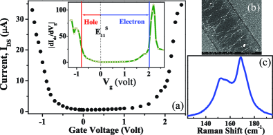
SWNTs are synthesized by arc-discharge followed by purification sample . AC dielectrophoresis dielectrophoresis is used to align and connect the nanotubes between two gold electrodes at 15 m separation. The average diameter of the bundles connected to the electrodes is 10-50 nm from the SEM image, Fig. 1(b). We have used as gating material a solid-polymer electrolyte electrolyte1 ; electrolyte2 prepared by dissolving LiClO4 and PEO (1:0.12) in methanol to form a precursor. The gate is applied by placing a platinum electrode into the polymer layer. The advantage of the solid electrolyte over the electrolytes in solution phase is that it does not degrade the sample and electrodes and the gate-current is extremely small (nA) even at high gate voltages (1V). A DILOR triple grating spectrometer equipped with charge-couple device is used to record the Raman spectra using a He-Ne (1.96 eV) laser. Fig. 1(c) shows the RBM of our tubes. It has two bands with average diameter =1.4 and 1.6 nm. The laser at 1.96 eV is in resonance with EM11 of tube diameter 1.4 nm and lies in between the EM11 and ES33 of 1.6 nm diameter tubes kataura . Therefore, Raman spectra has contributions from metallic tubes of =1.4 nm as well as from both semiconducting and metallic tubes of =1.6 nm.
Fig. 1(a) shows the ambipolar behavior of our nanotube FET device at a drain-source voltage VDS of 50 mV. At gate voltage Vg=0, IDS 500 nA. The behavior of the current through the SWNT is reversible with Vg and the leakage current is very small ( 10 nA at V 2V). Since the current increases on either side of the starting zero Vg, we infer that the initial Fermi energy (=0) is at the middle of the gap of semiconducting tubes (charge neutrality point-CNP) electrolyte2 . The sharp increase in current, as shown in Fig. 1(a), for large positive (negative) Vg is due to addition of electrons (holes) to the first van Hove singularity on conduction (valence) band side of the semiconducting tubes present in the sample along with the metallic tubes. The onset of this increase in current is observed for Vg=2.02 V and -0.8 V, inset of Fig. 1(a). For the semiconducting tubes of average diameter 1.5 nm, ES11 0.5 eV and for metallic tubes EM11 1.8 eV kataura . As the metallic tubes have larger energy separation between the van Hove singularities, the sharp increase in conductivity in Fig. 1(a) is mostly governed by the semiconducting tubes. Therefore, the semiconducting tubes of the sample act as an internal read out to estimate the Vg-induced shift. We define the proportionality factor (), to estimate at different positive (negative) gate voltages ( = Vg). For electron doping, a positive voltage of 2.02 V shifts into the first conduction band, which is 0.25 eV from the CNP. Therefore, = 0.25/2.02 = 0.12 and similarly = 0.25/0.8 = 0.31 . The difference between and is probably due to double layer formation of different ions Li+ and ClO4- in PEO matrix at the interfaces.
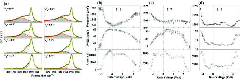
Fig. 2(a) shows the Raman spectra recorded at different Vg. A constant gate voltage is applied for 15 minutes to stabilize IDS and then the Raman spectra were recorded for next 15 minutes at the same Vg. For a Vg in the -1.25/+2.5 V range, the Raman spectra as well as the source-drain current fully recover to the starting condition (Vg=0) within about one hour after removing the gate voltage. There are three prominent Raman modes and the spectra are fitted with three Lorentzians L1 (1540 cm-1), L2 (1567 cm-1) and L3 (1590 cm-1). The Raman frequency, linewidth and total area thus obtained for L1, L2 and L3 modes are plotted in Figs. 2(b), 2(c) and 2(d), as a function of Vg. Following Fig.19 of Ref. kohnanomalynt , the L1 line is attributed to the LO mode of the metallic tubes with diameter 1.4 nm kohnanomalynt . The L1 line can be equally well fitted by a Lorentzian or a Fano-resonance line-shape. We use a Lorentzian line-shape to minimize the number of fitting parameters. In our spectra, the L2 has a large line-width of 40 cm-1 and the doping dependence is similar to that of L1 mode. Therefore the L2 line is attributed to a combination of the LO mode of metallic tubes and of the TO mode of semiconducting tubes with diameter 1.6 nm (Fig.19 of Ref. kohnanomalynt ). The L3 line is attributed to a combination of the TO of metallic and the LO of semiconducting tubes. The EPC determines an important broadening of the LO mode of metallic tubes epc . This explains the large width of the L1 ( 60 cm-1) and L2 ( 40 cm-1) lines. The sharpness of the L3 line ( 10 cm-1) is explained considering that the semiconducting LO and the metallic TO modes are not broadened by EPC and that their frequencies are almost independent from diameter (Fig.19 of Ref. kohnanomalynt ).
As shown in Fig. 2(b), the largest effect is the frequency increase of the L1 line by 15/10 cm-1 on hole/electron doping. The substantial decrease of its linewidth is also remarkable. Both effects are due to the dependence of the KA on Vg in metallic tubes. The L2 line displays a similar behavior due to the metallic tubes associated with this line. The intensity of the L1 line (entirely due to metallic tubes) drops to zero at high doping (positive or negative). This suggests that, at high doping, the Raman signal from metallic tubes is neglegible. Thus, the behavior of the L3 line at high doping is mostly due to semiconducting tubes. Interestingly, the frequency upshift of the L3 line is perfectly correlated to the IDS current (Fig.1), indicating that the L3 shift is due to the change of the electron (hole) populations in the conduction (valence) bands of semiconducting tubes.
We now compare measurements with DFT calculations, done using i) the adiabatic Born-Oppenheimer approximation (BOA, Eq.6 of Ref. lazzeri06 ) and ii) time-dependent perturbation theory (TDPT, Eq.7 of Ref. lazzeri06 ) to include dynamical effects beyond BOA. Within BOA, the phonon frequency is obtained from the forces resulting from a static displacement of the atoms. However, a phonon is not a static perturbation to the system but a dynamic one, oscillating in time, that should be treated within TDPT. Dynamic effects beyond BOA are usually assumed to be neglegible, but they are crucial to reproduce the Raman spectra of nanotubes and doped graphene kohnanomalynt ; kohnanomalydopednt ; lazzeri06 ; pisana07 . Our DFT calculations are based on a linear response approach dfpt as described in Ref. kohnanomalydopednt . Calculations are done on a metallic (10,10) and on a semiconducting (20,0) tube, having diameters 1.4 and 1.6 nm. We compute the variation of the LO and TO phonon frequency ( and ) as a function of the doping. We also compute the intrinsic linewidth ( and ) due to EPC (Eq.29 of Ref. kohnanomalydopednt ), owing to the decay of the phonon into electron-hole pairs, which is nonzero only for metallic tubes. The electronic occupations are determined according to a Fermi Dirac distribution at 315 K.

For metallic tubes and are negligible, since the EPC between occupied and empty electronic states is zero (see Eq.9 of Ref. kohnanomalydopednt ). For diameter larger than 1 nm, , and are universal, i.e. independent of both and chirality epc ; kohnanomalydopednt . Fig.3 reports these universal behaviors, as functions of , computed within TDPT. BOA results are not reported, since they are very similar for eV kohnanomalydopednt . The hardening of for is understood by considering the modification of the electronic band structure in the presence of the LO phonon. An atomic distortion following the LO phonon pattern opens a gap at the CNP dubay02 . The filling of the electronic states with doping increases the energy required to open this gap, thus inducing a hardening of the LO frequency footnotehardening .
We assume that has a Gaussian distribution (with a standard deviation ) to take into account the spatial fluctuation of in the actual device. In Fig. 3 we report the average frequency and the FWHM of the LO peak profile obtained by an ensemble of tubes with such a distribution. To include the experimental data in Fig. 3 we multiply the measured Vg by and . The calculations best describe the experiment with eV. The agreement between theory and measurements is excellent for . The theoretical LO linewidth is smaller than the experimental one, probably because of other effects, such as the finite diameter distribution.

In semiconducting tubes, and depend on the positions of the band edges, i.e. on and, to a lesser extent, on the chirality. Fig. 4 shows and computed within BOA and TDPT. Within the more accurate TDPT, and upshift when reaches the vHs. To understand this behavior, we have to consider how the electrons screen a phonon vibration. The electronic screening can be expressed in terms of interband and intraband EPC transitions between electronic states lazzeri06 . Within TDPT only the interband transitions between occupied valence and empty conduction electronic states contribute (Eq.(7) of lazzeri06 ). By doping the tube, the valence (conduction) band is emptied (filled). Both processes correspond to a reduction of the number of allowed transitions. The consequent reduction of the screening upshifts . The shift is more pronounced for the TO phonon that has a larger EPC for transition beween valence and conduction band edges. Within BOA, the presence of intraband transitions (second line of Eq. (6) of lazzeri06 ) contrasts the hardening due to interband transition lazzeri06 ; kohnanomalydopednt .
The of both metallic and semiconducting tubes are affected in a different way by Vg. Thus, the behavior of of semiconducting tubes in the L2 line cannot be separated from that of metallic tubes. We can instead directely compare the theoretical with the L3 line, since, at small doping, the position the of both metallic and semiconducting tubes does not depend on Vg and, at large doping, the metallic-tube intensity vanishes. TDPT calculations for the LO mode compare very well with the mesured behavior of the L3 line, that we report in Fig. 4 using the transport-derived ratios , . At the minumum Vg, L3 upshifts by 5 cm-1. According to TDPT, this corresponds to a doping of holes per C atom and to -0.15 eV shift of below the first vHs.
Concluding, by combining transport, in-situ Raman experiments and ab-initio calculations we quantified the effect of the doping on the phonons in carbon nanotubes. By electron and hole doping, the Raman peak of metallic tubes and both the and of semiconducting tubes harden. Moreover, the linewidth of metallic tubes narrows. Important consequences of the present results are that: i) The metallicity of the system is not always associated with the presence of a broad peak, as often assumed. Indeed, in a doped metallic tube, the -peak width can be much smaller than in the undoped case if the Fermi level is far from the band-crossing. ii) Given the strong dependence of the Raman bands on the Fermi energy, Raman spectroscopy can be used as an accurate measure of the doping of both metallic and semiconducting nanotubes, with important technological implications for nano electronics.
AKS thanks DST, India for support. Calculations were performed at IDRIS (France), project CP9-61387/71387, using the quantum-espresso package (www.pwscf.org).
References
- (1) S. Reich, C. Thomsen, and J. Maultzsch, Carbon nanotubes: basic concepts and physical properties, (Wiley-VCH, 2004)
- (2) R. Saito, G. Dresselhaus, and M.S. Dresselhaus, Physical properties of carbon nanotubes, (Imperical College Press, 1998)
- (3) S. Tans, A. Verschueren, and C. Dekker, Nature 393, 49 (1998).
- (4) S. Ghosh, A.K. Sood, and N. Kumar, Science 299, 1042 (2003).
- (5) O. Dubay, G. Kresse, and H. Kuzmany, Phys. Rev. Lett. 88, 235506 (2002).
- (6) S. Piscanec et al., Phys. Rev. B 75, 035427 (2007).
- (7) M. Lazzeri et al., Phys. Rev. B. 73, 155426 (2006).
- (8) S. Piscanec et al., Phys. Rev. Lett. 93, 185503 (2004).
- (9) M. Lazzeri and F. Mauri, Phys. Rev. Lett. 97, 266407 (2006).
- (10) S. Pisana et al. Nature Materials 6, 198 (2007); J. Yan et al., Phys. Rev. Lett. 98, 166802 (2007).
- (11) N. Caudal et al., Phys. Rev. B 75, 115423 (2007).
- (12) M. Stoll et al., Chem. Phys. Lett. 375, 625 (2003).
- (13) L. Kavan et al., J. Phys. Chem. B. 105, 10764 (2001).
- (14) N. Bendiab et al., Phys. Rev. B. 64, 245424 (2001).
- (15) C.P. An et al., Synth. Met. 116, 411 (2001).
- (16) P. Corio et al., Chem. Phys. Lett. 370, 675 (2003).
- (17) P.M. Rafailov et al., Phys. Rev. B. 72, 045411 (2005).
- (18) M. Krüger et al., Appl. Phys. Lett. 78, 1291 (2001).
- (19) C. Lu et al., Nano Lett. 4, 623 (2004).
- (20) G.P Siddons et al., Nano Lett. 4, 927 (2005).
- (21) S.R.C. Vivekchand et al. Small 1, 920 (2005).
- (22) R. Krupke et al. Science 301, 344 (2003).
- (23) T. Michel et al. Phys. Rev. B 75, 155432 (2007).
- (24) S. Baroni et al. Rev. Mod. Phys. 73, 515 (2001).
- (25) The behavior of in metallic tubes can be equally understood within perturbation theory, in terms of interband electronic transitions, as we explained in ref. kohnanomalydopednt . Here we adopt this approach to interpret the behavior of the semiconducting tubes.