Thickness-dependence of the electronic properties in V2O3 thin films
Abstract
High quality vanadium sesquioxide V2O3 films (170-1100 Å) were grown using the pulsed laser deposition technique on (0001)-oriented sapphire substrates, and the effects of film thickness on the lattice strain and electronic properties were examined. X-ray diffraction indicates that there is an in-plane compressive lattice parameter (), "close to -3.5% with respect to the substrate" and an out-of-plane tensile lattice parameter () . The thin film samples display metallic character between 2-300 K, and no metal-to-insulator transition is observed. At low temperature, the V2O3 films behave as a strongly correlated metal, and the resistivity () follows the equation =, where is the transport coefficient in a Fermi liquid. Typical values of have been calculated to be 0.14 cm K-2, which is in agreement with the coefficient reported for V2O3 single crystals under high pressure. Moreover, a strong temperature-dependence of the Hall resistance confirms the electronic correlations of these V2O3 thin films samples.
pacs:
81.15.Fg, 71.27.+a, 74.20.Mn, 68.55.-aFirst discovered by Foex in 1946,foex46 vanadium sesquioxide V2O3 has received a great deal of attention, both by theoreticians as well as experimentalists. Indeed, it has been recognized previously that a pressure-induced metal-to-insulator transition (MIT) for V2O3 is driven by electron correlation, mott49 establishing V2O3 as a prototypical strongly correlated electron system. As a result, numerous studies on the effect of composition or external parameters on the transport properties of V2O3 have been reported.whan73 ; yethiraj90 ; limelette2003 Particular attention has been also paid to the phase transitions of V2O3: in the pressure-temperature plane two phase transitions are reported, either when applying a hydrostatic pressure or a chemical pressure (see for example, (V1-xMx)2O3 with M=Cr, Ti,..).whan73 ; yethiraj90 For example, a system that is close to all phase boundaries is (V0.985Cr0.015)2O3 at 200 K.kuwamoto80 When the temperature is decreased, this paramagnetic metal undergoes a first order phase transition from a corundum structure with rhombohedral symmetry ( space group, with a=4.951 Å, c=14.003 Å) to an antiferromagnetic insulator with monoclinic structure ().dernier70 When the temperature or the Cr-content is increased, a paramagnetic metal to paramagnetic insulator transition takes place.kuwamoto80 While the former transition bears strong similarities with many usual magnetic transitions, the latter one corresponds to the famous Mott transition. Qualitatively, this Mott transition is well described by the Hubbard model: increasing the Cr-content results in increasing the ratio ( being the strength of the Coulomb interaction, and the bandwidth), in which case the quasiparticle residue decreases, and eventually vanishes at the MIT.Brinckman Furthermore, when considering the optical conductivity, the optical weight at low energy is transfered to energies of order .Thomas When the system is close to the Mott point, thermal fluctuations destabilize the coherence of the Fermi liquid (FL), and an increase in temperature results into a MIT.Spalek ; georges96 ; fresard97 Several orbitals are involved at the Fermi energy, and however, a quantitative description of V2O3 needs to build on a more involved theory, such as the one pioneered by Held et al.Held
Despite extensive studies on polycrystalline powder and single crystal V2O3 samples,whan70 ; ueda80 ; shivashankar83 ; whan69 there have been few reports on thin film samples. Schuler et al. addressed the influence of the synthesis conditions upon the classical metal-to-insulator transition and the growth modes of the films.schuler97 The relation between the transition temperatures and the lattice parameters also have been reported.autier2006 ; yonezawa2004 ; luo2004 There is little knowledge however on the thickness-dependence of the properties of the V2O3 thin films.
In this letter, we examine a series of epitaxial V2O3 thin films, including their lattice parameters, roughness, and Hall resistance, in order to investigate their transport properties as a function of thickness.
Samples of V2O3 thin films, of which the thickness ranged from 170 Å to 1100 Å, were grown on (0001)-oriented Al2O3 substrates (rhombohedral with the parameters, a=4.758 Å, c=12.991 Å) by the pulsed laser deposition technique. A pulsed KrF excimer laser (Lambda Physik, Compex, =248 nm) was focused onto a stoichiometric V2O5 target at a fluence of 4 J cm-2 with a repetition rate of 3 Hz. The substrate heater was kept at a constant temperature ranging from 600∘C to 650∘C. A background of argon pressure around 0.02 mbar was applied inside the chamber. At the end of the deposition, the film was cooled down to room temperature at a rate of 10 K min-1 under a 0.02 mbar argon pressure. The film thickness was determined, to an uncertainty below two V2O3 unit cells, by a mechanical stylus measuring system (Dektak3ST). The structure of the films was examined by X-Ray Diffraction (XRD, with the Cu K radiation, =1.54056 Å) using a Seifert 3000P diffractometer for the out-of-plane measurements and a Philips X’Pert for the in-plane measurements. In-plane a lattice parameters were extracted from (104), (116), (113) asymmetric reflections. The resistivity of the samples were measured in four probe configuration using a PPMS system. To make appropriate connections onto the film, four silver plots were first deposited via thermal evaporation onto the film, and then thin aluminum contact wires were used to connect these areas to the electrodes. For Hall effect measurements, a Van der Pauw configuration of silver plots was used. For each temperature value, the transverse resistance is measured with an applied magnetic field varying from -7 T up to +7 T. The Hall resistance RH is calculated from the transverse resistance () using the formula RH=, where is the applied magnetic field.
As it is known that the nonstoichiometry can drastically influence the electric properties of V2O3,ueda80 a X-ray photoelectron spectroscopy study was carried out. It shows that the oxidation state of vanadium can be estimated around , confirming that the films stoichiometry is close to V2O3.autier2006 scans XRD measurements reveal that only the peaks corresponding to the 00l reflections (where =6, 12…) are present, which indicates that the -axis of the films is perpendicular to the plane of the substrate. -scans, recorded around the (104) reflection show three peaks separated by 120∘ from each other, indicating that the films have a 3-fold symmetry and are grown epitaxially, with respect to the substrate. These results are in agreement with the rhombohedral symmetry observed in the bulk V2O3. This symmetry and the space group are further confirmed by electron diffraction pattern analyses. The high quality of the films was also attested by the low value of the rocking-curve close to (0.20∘) measured around the (006) reflection of the film.

Fig. 1 displays the evolution of the lattice parameters () and (), characteristic of the structure, as a function of the thickness . The out-of-plane lattice parameter () is slightly larger than the bulk values, by 0.450.1 %, while the in-plane () is smaller by -0.550.1 %, confirming a biaxial compression in the (ab) plane, estimated to -3.50.5 % with respect to the substrate (the stress values are calculated from the mean-values () and () obtained from the thickness dependence in Fig. 1). This suggests an anisotropic strain similarly to previous reports.yonezawa2004 Surprisingly, the lattice parameters are almost independent of , indicating that the films are fully strained in the whole thickness range. The surface morphology was also studied by Atomic Force Microscopy (AFM) with a scan area of m2. Topography of the V2O3 samples reveals that the roughness increases when the thickness increases. For example, a typical surface roughness (rms) of 4.5 Å was observed for the thinnest film (170 Å), while a thicker sample (700 Å) has a rms value of 11 Å. This may indicate that the growth mode is mixed: a layer-by-layer (2D-mode) on the (ab) plane at the initial step of the growth, and an island coalescence (3D-mode) along the c-axis when the thickness increases. To summarize, the structural and microstructural analyses confirm that the films crystallize in the structure, as in bulk, despite a large in-plane compressive strain.
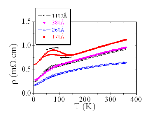
The longitudinal resistivity () of V2O3 films is plotted in Fig. 2 as a function of temperature for several thicknesses. In contrast to bulk samples, none of the investigated films exhibit a strong temperature-dependent resistivity. This is especially valid for 220 Å, in which case the resistivity increases continuously with temperature as in a metal. Nevertheless, some hysteresis is observed, though strongly suppressed with respect to the bulk. Thus, we can conjecture that the abovefound stress in the (ab) plane results into a larger band width, and hinders the paramagnetic metal-to-antiferromagnetic insulator transition. In contrast, for thinner films (t < 220 Å), the films are metallic with a weak increase of the resistivity near . Its origin might be a reminder of the structural transition.
| (Å) | (m cm) | (K) | (cm-3) | (cm2 (V s)-1) | |
|---|---|---|---|---|---|
| 1100 | 0.24 | 19.6 | 18.7 | 4.5 | 0.160.05 |
| 380 | 0.27 | 14.0 | 17.5 | 4.4 | 0.150.06 |
| 260 | 0.19 | 10.2 | 15.8 | 4.9 | 0.210.10 |
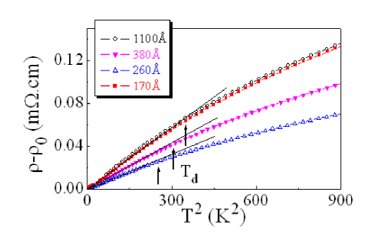
As shown in Fig. 3, resistivity data for all films follow a law in in the temperature range from up to a characteristic temperature . Here represents the (film dependent) residual resistivity, and the transport coefficient in a Fermi liquid. This behavior, which differs from simple metals that exhibit or behavior, is seldom observed over such a temperature range, except for a few strongly correlated electron system, such as Ca3Co4O9.limelette2005 Table 1 summarizes the values (), () and () for a series of films. The average value of is close to 0.14 cm K-2 across the whole thickness range, indicating that the coefficient is not significantly thickness-dependent. Moreover, it should be note that such values are similar to those measured for single crystal V2O3 samples subjected to high pressures (26-52 kbar).whan69 The high values involve the existence of strong electronic correlations in our metallic thin films. The product is about two orders of magnitude lower than , indicating that the FL behavior does not extend up to the effective Fermi temperature. Instead, an additional scattering channel opens up at > , which might be provided by spin fluctuations. To better quantify the temperature range where this scattering channel is relevant, we performed Hall effect measurements in the temperature range 2-300 K. Fig. 4 shows the resulting Hall resistance () for a series of films.

The positive slope of the Hall resistance implies hole-like charge carriers, as inferred by McWhan et al.whan70 Moreover, while the Hall resistance would be nearly temperature independent in a regular metal, it here exhibits a strong temperature dependence, especially for < 200 K. In particular, the strain involved in our films has little influence on the location of the maximum of RH, as it is located at a temperature very close to the one reported for metallic bulk samples.carter93 Nevertheless, this temperature slightly increases as the thickness decreases. A similar result has been observed in the aforementioned single crystals with an increase in pressure, indicating that the decrease of the thickness is consistent with an increase of the pressure. At room temperature, in the temperature-independent regime, the values of the carriers number () and Hall mobility () can also be extracted from the Hall resistance value (see Table I). For the thicker film (1100 Å), they are calculated to be and =0.160.05 cm2 V-1 s-1, which are consistent with the ones observed in V2O3 single crystals.whan70 Note that looses its temperature-dependence above 200 K, which indicates that above this temperature the correlation length of the fluctuations that scatter the electrons become of the order of the lattice parameter. Consequently, in this regime, the resistivity is expected to be -linear, which is indeed observed for most of the films.
In summary, high quality epitaxial V2O3 thin films were grown, with thickness ranging from 170-1100 Å, by pulsed laser deposition on sapphire substrate (0001-Al2O3). Using multiple of characterization techniques, we confirm that the films have the same rhombohedral structure ( space group) as in the bulk despite the substrate-induced strains. The thickness-dependence of the electronic properties show the suppression of the classical metal-to-insulator transition with a metal-like behavior. At low temperature, the dependence of the resistivity as a function of was measured to be that of a strong correlated metal, and was confirmed by temperature-dependence of the Hall resistance.
We thank D. Grebille and A. Pautrat for fruitful discussions. J.F. Hamet and Y. Thimont are also acknowledged for the AFM measurements. This work is carried out in the frame of the STREP CoMePhS (NMP3-CT-2005-517039) supported by the European community and by the CNRS, France.
References
- (1) M. Foex, C. R. Acad. Sci. 223, 1126 (1946).
- (2) N. F. Mott, Proc. Phys. Soc. A 62, 416 (1949).
- (3) D. B. McWhan, A. Menth, J. P. Remeika, W. F. Brinkman, and T. M. Rice, Phys. Rev. B 7, 1920 (1973).
- (4) M. Yethiraj, J. Solid State Chem. 88, 53 (1990).
- (5) P. Limelette, A. Georges, D. Jérome, P. Wzietek, P. Metcalf, and J. M. Honig, Science 302, 89 (2003).
- (6) H. Kuwamoto, J. M. Honig, and J. Appel, Phys. Rev. B 22, 2626 (1980).
- (7) P. Dernier and M. Marezio, Phys. Rev. B 2, 3771 (1970).
- (8) W. F. Brinckman and T. M. Rice, Phys. Rev. B 2, 4302 (1970).
- (9) G. A. Thomas, D. H. Rapkine, S. A. Carter, A. J. Millis, T. F. Rosenbaum, P. Metcalf, and J. M. Honig, Phys. Rev. Lett. 73, 1529 (1994).
- (10) J. Spałek, A. Datta, and J. M. Honig, Phys. Rev. Lett. 59, 728 (1987).
- (11) A. Georges, G. Kotliar, W. Krauth, and M. J. Rozenberg, Rev. Mod. Phys. 68, 13 (1996).
- (12) R. Frésard and G. Kotliar, Phys. Rev. B 56, 12 909 (1997).
- (13) K. Held, G. Keller, V. Eyert, D. Vollhardt, and V. I. Anisimov, Phys. Rev. Lett. 86, 5345 (2001).
- (14) D. B. McWhan and J. P. Remeika, Phys. Rev. B 2, 3734 (1970).
- (15) Y. Ueda, K. Kosuge, and S. Kachi, J. Solid State Chem. 31, 171(1980).
- (16) S. A. Shivashankar and J. M. Honig, Phys. Rev. B28, 5695 (1983).
- (17) D. B. McWhan and T. M. Rice, Phys. Rev. Lett. 22, 887 (1969).
- (18) H. Schuler, S. Klimm, G. Weissmann, C. Renner, and S. Horn, Thin Solid Films 299, 119 (1997).
- (19) S. Autier-Laurent, B. Mercey, D. Chippaux, P. Limelette, and Ch. Simon, Phys. Rev. B 74, 195109 (2006).
- (20) S. Yonezawa, Y. Muraoka, Y. Ueda, and Z. Hiroi, Sol. State Comm. 129, 245 (2004).
- (21) Q. Luo, Q. Guo, and E. G. Wang, Appl. Phys. Lett. 84, 2337 (2004).
- (22) P. Limelette, V. Hardy, P. Auban-Senzier, D. Jérome, D. Flahaut, S. Hébert, R. Frésard, Ch. Simon, J. Noudem and A. Maignan, Phys. Rev. B71, 233108 (2005).
- (23) S. A. Carter, T. F. Rosenbaum, P. Metcalf, J. M. Honig and J. Spałek, Phys. Rev. B48, 16841 (1993).