Periodically rippled graphene: growth and spatially resolved electronic structure
Abstract
We studied the growth of an epitaxial graphene monolayer on Ru(0001). The graphene monolayer covers uniformly the Ru substrate over lateral distances larger than several microns reproducing the structural defects of the Ru substrate. The graphene is rippled with a periodicity dictated by the difference in lattice parameter between C and Ru. The theoretical model predict inhomogeneities in the electronic structure. This is confirmed by measurements in real space by means of scanning tunnelling spectroscopy. We observe electron pockets at the higher parts of the ripples.
pacs:
73.20.-r, 68.37.Ef, 68.55.-a, 81.05.UwThe possibility to produce single layers of graphene Novoselov ; Geim has opened a fascinating new world of physical phenomena in two dimensions. Graphene has already shown that its charge carriers are massless Dirac fermions Novoselov1 ; Zhang ; Novoselov2 ; Gusynin ; Peres and that it displays an anomalous integer Quantum Hall Effect Novoselov1 ; Zhang ; Novoselov2 even at room temperature Novoselov3 . Systems made up of a few graphene layers can also be grown on a SiC substrate Berger ; Rutter . Recently it has been shown that free standing isolated graphene layer is intrinsically corrugated Meyer . These modulations in the heights of the graphene layers may be related to the charge inhmogeneities observed in nominally undoped samplesMetal07 (seeNG07 ).
Ultra-thin epitaxial films of graphite have been grown on solid surfaces for quite some time Oshima . Even the growth of ”monolayer-graphite” films onto several substrates by Chemical Vapor Deposition have been reported some time ago, but the degree of characterization of the films was hampered by the existing experimental limitations Hu .
In this letter we report on a method to fabricate highly perfect, on the scale of microns, periodically rippled graphene monolayer and islands on Ru(0001) under Ultra High Vacuum (UHV) conditions. We characterized by means of scanning tunnelling microscopy/spectroscopy (STM/STS) the perfection at atomic scale and the local electronic structure of the periodically rippled graphene monolayer. The periodicity of the ripples is dictated by the difference in lattice parameters of graphene and substrate, and, thus, it is adjustable. We observe inhomogeneities in the charge distribution, i.e electron pockets at the higher parts of the ripples. This inhomogeneity in the electronic structure can be understood with the help of a tight-binding model. The potential associated with the rippled structure induce a charge transfer from conduction to valence bands for some atoms and the opposite in the others. Finally we studied graphene nanoislands that display hexagonal shape with atomically resolved zigzag edges, whose characteristic edge states allows us to determine the doping of the graphene layer.
The experiments have been carried out in a UHV chamber with base pressure of 4 Torr that contains a variable temperature STM and a rear view Low Energy Electron Diffraction (LEED) optics. The Ru(0001) crystal was cleaned by cycles of sputtering and annealing followed to oxygen exposure and heating to high temperature Calleja . The graphene layers were produced either by controlled segregation of C from the bulk of the substrate or by thermal decomposition at 1000 K of ethylene molecules pre-adsorbed at 300 K on the sample surface. The W tips were routinely cleaned by ion bombardment and annealing. The curves were obtained by numerical differentiation of the curves. We model the graphene electronic bands by a nearest neighbor tight-binding model with parameter t=3eV, a periodic shift of the carbon pz levels, and a finite broadening due to the hybridization with the metallic substrate. In order to calculate the density of states, we use a (3030) unit cell, and a sum over 6 special points in the irreducible sector of the Brillouin zone. Hence, the total number of states included in the calculation is 10800. This is sufficient to resolve local changes in the electron density in the order of 10-2-10-3 carriers per carbon atom.
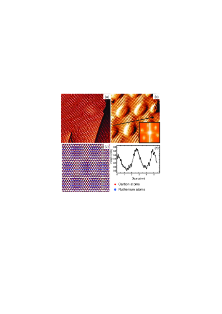
The epitaxial layer of graphene covers completely the surface of the single-crystal Ru substrate over distances larger than a micron (see micron ) and presents a triangular periodicity of 2.4 nm (Fig. 1(a)) that is due to the coincidence lattice of graphene and Ru, i.e. the lattice of graphene is incommensurate with the underlying lattice of Ru, with a size relation that implies that 10 carbon honeycombs (0.246 nm) will adjust almost exactly with 9 Ru-Ru interatomic distances (0.27 nm). The weakly interacting (see below), laterally undistorted graphene structure rides on top of the lattice of the substrate, resulting in some C atoms being somewhat higher than others. The graphene layer, thus, is rippled in a periodic fashion, with a periodicity dictated by the difference in lattice parameters. Variations of this approach using other experimental conditions can be used to produce graphene monolayers on other single-crystal substrates Fujita .
With the STM images we characterize the type of defects that appear in the epitaxial graphene layer. The monoatomic steps and dislocations of the substrate are reproduced, but there are also upper part of the ripples that are weaker or even missing completely in the STM images, as can be seen in Fig. 1 (a) and in ref. movie . Fig. 1 (b) shows a high resolution topographic STM image of the epitaxial graphene layer, revealing its atomic structure. Unlike STM images of graphite Sinitsyna , which show normally only one of the two C atoms in the surface unit cell, the honeycomb structure of graphene is clearly resolved in the upper part of the ripples with its 0.14 nm C-C distance. The Fourier transform of larger atomically resolved STM images shown as inset in Fig. 1(b) indicates that the ripples constitute a (1010) superlattice with respect to the C lattice. The (99) coincidence lattice with the Ru(0001) substrate is revealed in the corresponding LEED pattern (not shown).

The apparent vertical corrugation of the rippled graphene monolayer, as seen with STM, changes with the tunnelling voltage, ranging from 0.1 nm (at a sample voltage of -1 V) to 0.02 nm (at +1 V). This indicates the importance of electronic effects. The C-C apparent atomic corrugation inside the honeycomb unit cell is only of the order of 0.005 nm (Fig 1(d)). The actual geometric corrugation of the rippled layer can be estimated to be below 0.02 nm from the observed lack of diffracted peaks for a beam of thermal He atoms scattering off the graphene surface Nieto .
The bonding with the substrate occurs through the hybridization of the C -states with the Ru d states. Photoelectron spectroscopy shows clearly that the layer bonding is not carbidic. Angular Resolved Photo Electron Spectroscopy data show that the graphene bands in graphene/Ru(0001) are similar to the ones of graphite, but rigidly shifted down in energy Himpsel . The bottom of the band at the center of the Brillouin Zone is shifted down by 1.8 eV with respect to graphite Himpsel . The small energy shift of the C1s core level with respect to graphite indicates that the charge transfer from the substrate is small, but not negligible, i.e. the graphene layer is doped with electrons by the substrate.
The graphene-Ru interface is atomically well defined. The average interlayer distance for the closely related incommensurate graphene/Pt(111) system has been determined to be rather large (0.37 nm) by means of tensor LEED analysis Hu . First principles calculations in the similar graphene/Ir(111) system have indicated that the average binding (0.2 eV/C atom) is barely strong enough to correspond to chemical bond formation Diaye . The incommensurate nature of the graphene monolayer is an additional indication that the interaction of graphene with the substrate is rather weak.
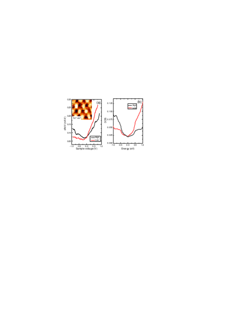
Fig. 2(a) shows spatially-resolved tunnelling spectra, which are roughly proportional to the Local Density of States (LDOS), recorded on top of the ”high” and ”low” regions of the corrugated graphene layer. Panel (b) shows the corresponding calculation. The experimental tunnelling spectra recorded at different spatial positions are obviously different: the occupied LDOS is systematically larger in the ”high” areas of the rippled layer, while the empty LDOS is larger in the ”low” parts. The differences are robust enough to survive at 300 K. There are also weaker features at both sides of the Fermi level, separated from each other by 0.3 eV and located at about the same energies in both regions of the ripples.

The electronic structure has been simulated by taking into account that the rippled graphene layer is not too distorted. The model calculations have been performed for an isolated graphene layer in which the effect of the substrate has been considered to result in: i) a shift of the Dirac point by -0.3 eV due to doping; ii) the introduction of a finite lifetime caused by hybrization of the orbitals with the band of the substrate; and iii) a (1010) periodic potential that changes between -3V and 3V/2,where V=-0.3eV to account for the periodic structural ripples. This value for the potential gives the better agreement with the experiments. For higher values of the potential the asymmetry in the calculated DOS is bigger than the one found in the experiments. The band in graphene has a total width of W6t, where t3 eV is the hopping between orbitals at nearest neighbor C atoms Brandt .
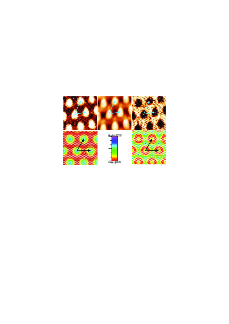
In agreement with the experiments, the calculations show that the occupied LDOS is larger on the ”high” regions of the superlattice, where the potential is at a minimum, while the empty LDOS is larger at the ”low” regions of the graphene layer(see lower panel in Fig. 3). This effect is extremely robust and indicates that the valence band is depleted in the low portions of the ripples, while the conduction band is depleted at the high parts of the ondulated graphene layer. The calculations also reproduce the weaker features at both sides of the Fermi energy that reflect the existence of the periodic superlattice, which induces a folding of the graphene bands in the new (1010) Brillouin Zone. The reconstruction consider here does not superimpose the two inequivalent corners of the Brillouin zone and it does not open a gap at the Dirac energy Manes . The spectrum is split on subbands separated by gaps, away from the K and K’ points.
The periodic charge inhomogeneities in the graphene layer can be visualized directly in the real space by imaging the spatial distribution of close to the Fermi energy. Fig. 3 shows the spatial distribution of the LDOS below and above the common Fermi level (which corresponds to the shifted neutrality level of the doped graphene layer). The experimental images are in the upper row at the left and the right of the corresponding topographic image. The bright regions correspond to larger LDOS. For a complete set of spatially resolved maps versus sample bias voltage see ref. movie .

These inhomogeneities in the charge distribution produced by the periodic ripples are probably also present in the structural corrugations inherent to free standing, isolated graphene monolayers Meyer .
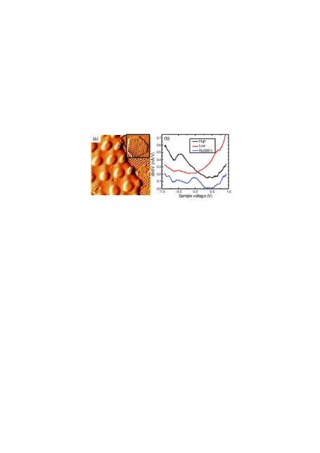
The growth method described here can also be used to produce different graphene nanostructures, such as nanowires on vicinal surfaces or nanometer wide islands as illustrated in Fig. 4(a). The apparent step height of the island is 0.15 nm (from the Ru surface to the lower part of the ripples) showing that the graphene layer is indeed only one monolayer high. The inset shows that the islands are truncated hexagons with straight edges of a single structural type. It is remarkable that the periodically rippled coincidence lattice goes right to the steps of the islands. In fact in some cases the island step cuts the (1010) arrangement. This confirms that the overlayer of graphene is indeed weakly coupled to the Ru substrate. Further zooming into the island reveals that the geometry of the steps is of the zigzag type.

The relative orientation of the graphene layer with respect to the underlying Ru lattice can be determined by resolving simultaneously both atomic lattices. In order to facilitate the resolution of the weakly corrugated Ru lattice, CO has been adsorbed at saturation in the parts of the Ru surface not covered by graphene. The geometry of the resulting ( R30∘) structure of CO on Ru(0001) is well known Gsell , and, thus, the relative orientation of graphene and Ru lattices represented in Fig. 1 has been obtained.
Fig. 4(b) shows local tunnelling spectra recorded when the surface is only partially covered with graphene. The advantage of this situation is that one can take spectra in the clean Ru patches of the surface, where only the surface state of Ru should be detected, and, thus, spurious features from the tip DOS can easily be detected. The spectra recorded at the center of the islands are undistinguishable from the one obtained on extended graphene layers (see Fig. 2). The spectra taken at the edges, however, show a new peak at -0.4 eV, particularly on the ”high” areas of the ripples, which might be related to the theoretically predicted edge states edge . The spectrum recorded on the clean Ru patches show only the surface state around the Fermi energy observed on Ru(0001) Calleja .
In summary we have grown graphene monolayers and islands on Ru(0001). The graphene monolayer presents a periodically rippled surface due to the difference in lattice parameter between graphene and the metallic substrate. The periodic ripples produce a spatial charge redistribution in the graphene. This have been measured with spatially resolved maps and confirmed with a theoretical model. The new periodicity also induce the opening of a series of minigaps by the additional periodic potential. The presence of these minigaps is expected to give rise to new phenomena at low temperatures in the presence of high magnetic fields. We atomically resolve the zig-zag edges of graphene islands and we use the position in energy of the edge state to determine the doping of the graphene layer. The methods described here can be implemented on many other single crystal substrates, giving rise to a series of graphene monolayers with different, substrate-dependent, periodic corrugations and, thus, opening the possibility to systematically test the electronic properties of controlled, charge inhomogeneous graphene layers. Methods to transfer the present finding to experimental systems adequate for lateral transport measurements are in progress.
Partial financial support by the Ministerio de Educación y Ciencia through projects MAT2003-08627-C02-02, NAN2004-08881-C02-01, FIS2005-05478-C02-01, the Comunidad de Madrid, through the programs CITECNOMIK, CM2006-S-0505-ESP-0337 and NANOMAGNET, S-0505/MAT/0194 and the European Union Contract 12881 (NEST), is gratefully acknowledged.
References
- (1) K.S. Novoselov et al., Science 306, 666 (2004).
- (2) A.K. Geim and K.S. Novoselov, Nature Mater. 6, 183 (2007).
- (3) K.S. Novoselov et al., Nature 438, 197 (2005).
- (4) Y. Zhang et al., Nature 438, 201 (2005).
- (5) K.S. Novoselov et al., Nature Phys. 2, 177 (2006).
- (6) V.P. Gusynin and S.G. Sharapov, Phys. Rev. Lett. 95, 146801 (2005).
- (7) N.M.R. Peres, F. Guinea and A.H. Castro Neto, Phys. Rev. B 73, 125411 (2006).
- (8) K.S. Novoselov et al., Science 315, 1379 (2007).
- (9) C. Berger et al., J. Phys. Chem. B 108, 19912 (2004).
- (10) G.M. Rutter et al., Science 317, 219 (2007).
- (11) J.C. Meyer et al., Nature 446, 60 (2007).
- (12) J. Martin et al., arXiv:0705.2180.
- (13) A. H. Castro Neto and E. A. Kim, arXiv:cond-mat/0702562, F. Guinea, M. I. Katsnelson, and M. A. H. Vozmediano, arXiv:0707.0682.
- (14) For a review see Ch. Oshima and A. Nagashima, J. Phys.: Condens. Matter. 9, 1 (1997).
- (15) Z.-P. Hu et al., Surf. Sci. 180, 433 (1987).
- (16) F. Calleja et al., Phys. Rev. Lett. 92 206101 (2004).
- (17) See EPAPS Document No. [] for a STM 1m 1m image of graphene on Ru(0001).
- (18) T. Fujita, W. Kobayashi and C. Oshima, Surf. Interf. Analysis, 37, 120 (2005).
- (19) O.V. Sinitsyna and I.V. Yaminsky, Russian, Chem. Rev. 75, 22 (2006).
- (20) P. Nieto et al. (in preparation).
- (21) F.J. Himpsel et al., Surf. Sci. Lett. 115, L159 (1982).
- (22) A.T. N’Diaye et al., Phys. Rev. Lett. 97, 215501 (2006).
- (23) N.B. Brandt, S.M. Chudinov and Y.G. Ponomarev, in Modern Problems in Condensed Matter Sciences, ed. V.M. Agranovich and A.A. Maradudin (North Holland 1988) Vol. 29.1
- (24) J.L. Mañes, F. Guinea and M.A.H. Vozmediano, Phys. Rev. B 75, 155424 (2007).
- (25) See EPAPS Document No. [] for a complete set of spatial resoved maps versus sample bias voltage in an energy range of 1 V.
- (26) M. Gsell, P. Jakob and D. Menzel, Science 280, 717 (1998).
- (27) Note that deviations from electron-hole symmetry away from the Dirac energy shift these states away from the neutrality point, see N.M.R. Peres et al. Peres .