Spin-Filtering Multiferroic-Semiconductor Heterojunctions
Abstract
We report on the structural and electronic properties of the interface between the multiferoic oxide YMnO3 and wide band-gap semiconductor GaN studied with the Hubbard-corrected local spin density approximation (LSDA+U) to density-functional theory (DFT). We find that the band offsets at the interface between antiferromagnetically ordered YMnO3 and GaN are different for spin-up and spin-down states. This behavior is due to the spin splitting of the valence band induced by the interface. The energy barrier depends on the relative orientation of the electric polarization with respect to the polarization direction of the GaN substrate suggesting an opportunity to create magnetic tunnel junctions in this materials system.
Multiferroics are materials in which ferroelectricity and magnetism coexist in a single phase. Efforts have shifted from the question of “coexistence”, to identifying strategies that will increase the coupling between the two orderings. This increased functionality opens opportunities for novel electrically or magnetically controlled devices. One route that is promising for practical applications is to employ multiferroic thin films and multilayered structures, the properties of which can be readily manipulated at the nanoscale.Ramesh07p21 ; Prellier05p803 Multiferroic YMnO3vanAken04p164 ; Fennie05p100103 is considered an attractive candidate for use in transistor devices because of its purity from volatiles such as Pb or Bi and its moderate dielectric constants.
Much effort has been directed at synthesizing and characterizing thin films of hexagonal YMnO3 as a potential gate dielectric for semiconductor devices, e.g.,YMnO3 on Si(111)Fujimura96p1011 ; Fujimura96p7084 ; Yoshimura98p414 ; Yi98p903 , on wurtzite GaN, or on ZnOPosadas05p171915 ; Chye06p132903 ; Bala06p1807 . Despite the remarkable progress in synthesis, the role of the interface strain, chemistry, etc., on the ferroelectric and magnetic properties of YMnO3 thin films is poorly understood and difficult to separate experimentally. In this Letter, we apply density-functional theory to calculate the electronic structure and band alignment at a realistic YMnO3/GaN interface. We demonstrate that interfacial spins behave differently from those in the bulk. This interface effect leads to a spin splitting in the valence bands giving rise to different band offsets for spin up and down states. Intriguingly, the difference in the band offsets depends on the polarization direction of YMnO3 relative to that of the polar GaN substrates, suggesting that the system could be utilized in spin-filtering tunneling junctions.

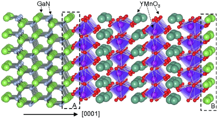
Bulk YMnO3 and wurtzite GaN both have hexagonal symmetry. YMnO3 is antiferromagnetic (AFM) and ferroelectric (FE) (space group ) while GaN is polar but not FE. X-ray diffraction of YMnO3 thin films deposited on GaN (0001) substrates suggests an in-plane rotation of 30∘ between the unit cell axes of YMnO3 and GaN. For a coherent interface this implies that YMnO3 is under a 10% in-plane compressive strain.Posadas05p171915 ; Chye06p132903 ; Bala06p1807 This large epitaxial strain has been attributed by Posadas et al. to the energy gain from the interfacial bond formation.Posadas05p171915 Here, we adopt the experimentally determined interfacial relation and build heterostructures composed of two unit cells of YMnO3 and GaN each, with a total of 24 atomic layers (Fig. 1). Both YMnO3/GaN interfaces are comprised of Ga and apical oxygens, coming from YMnO3 and GaN, respectively. The interfacial oxygens are placed above the fcc sites (i.e., the threefold cavity sites) of the Ga surface. The periodic boundary condition in our calculations creates two inequivalent Ga-O bonded interfaces between the sequence of YMnO3 and GaN, one with oxygens above the Ga (0001) face and another with oxygens above the Ga (000) face (see interfaces and in Fig.1 respectively).
We perform DFT calculations of YMnO3 within the LSDA+U approximation with eV and eV.note:VASP The value of was extracted from experiment (XPSKang05p092405 ). We obtain a band gap of 1.46 eV (1.47 eV)Kang05p092405 and lattice parameters of =6.09Å (6.127Å)vanAken01p230 and = 1.86 (1.86) which agree well with experiment (shown in parentheses). The Mn spins were treated in a frustrated collinear-AFM approximation as the 120∘ noncollinear spin structure observed in bulk YMnO3 is beyond the computational capabilities for the realistic interface that we consider here. For bulk GaN, we carried out LDA calculations and found = 3.15Å, , and . The LDA band gap is 2.1 eV, which is below the true value 3.5 eV. Since the Hubbard correction does not provide genuine improvement in GaN, we used a Hubbard U only on the Mn atom.
To isolate the effect of strain, we first relax bulk YMnO3 under in-plane compressive strain of . The -axis lattice parameter expands by 7%, consistent with Ref. Posadas05p171915, . The Mn moments are slightly reduced compared to the unstrained bulk value of . The distances between Mn and the in-plane oxygens MnOP shorten to Å, while the distances between Mn and the apical oxygens MnOA lengthen to Å, compared to Å and Å, respectively, in the unstrained bulk. Despite the significant shortening of the Mn-OP bonds, no changes occur to the topmost valence bands including OP , and Mn and orbitals as well as the unoccupied states. The most noticeable change occurs in the OA states and the OP states immediately below the OP bands, which downshift by eV near the point, presumably due to strain-induced buckling of MnO5 bipyramids.

Because wurtzite GaN is polar (a permanent dipole moment is produced by each bilayer of Ga+ and N-) we construct two supercells; “” with the FE polarization in YMnO3 pointing along GaN (000), and “” with the FE polarization pointing along GaN (0001). We then relax both supercells fixing the in-plane lattice constant to . In either supercell, the vertical distances between the apical oxygens and the Ga atoms at the and interfaces (see Fig.1) are drastically different, ranging from 1.11.2Å at interface to 0.20.6Å at interface . The different bonding structures of two interfaces agrees with the behavior of oxygen adatoms absorbed on Ga surfaces in the low oxygen coverage (growth) condition of GaN.Zywietz99p1695

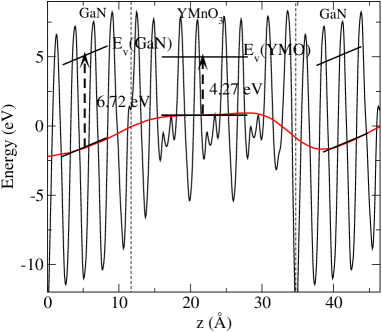
Fig. 2 shows the macroscopically averaged electrostatic potential the direction. The polarization field in GaN, evident from the slope of the electrostatic potential, induces charge transfer across the film and induces screening on the opposite sides of the GaN films. As a consequence, the residual field across YMnO3, parallel (antiparallel) to the field in GaN in supercell (), is small. Using the effective ionic charges,vanAken04p164 we estimate the polarizations of YMnO3 in the supercell to be C/cm2 for and C/cm2 for . These numbers are slightly lower than C/cm2 calculated for the constrained bulk (C/cm2 in unconstrained bulk)vanAken04p164 , indicating incomplete screening of the polarization charges at the interfaces. The polarization fields in these systems complicate comparison of the band edges directly from the lineup of the average potential as shown in Fig. 2
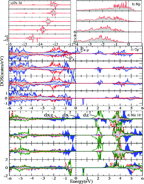
To analyze the electronic structure of the supercells we calculate the orbital-resolved, layer-projected density of states (PDOS). In the supercell, there is clearly a band bending of eV in GaN due to polarization, as illustrated by the deep Ga valence states in Fig. 3. The band bending is also evident in the topmost valence bands Np in Fig. 3 that produces an upward bending at interface and a downward bending at interface , consistent with the experiments in GaN (0001) films.Chevtchenko06p2104 Despite this bending, there is no sign of gap closing as the thickness of our GaN films is much below critical.Fiorentini99p8849 Fig. 3 and show the DOS for Mn and planar OP states. The interior layers look similar to the bulk layers, suggesting that the interior region converges to the bulk. The hole states at interface are composed of Mn , , OP and a small contribution from OA . At interface we observe a down shift in energy of the Mn orbitals (located at 2eV above in the bulk), and a strong overlap with the Op states. We encounter similar behavior in supercell except that the is eV deeper than in . The difference can be related to charge compensation at the interfaces: in , the polarizations of YMnO3 and GaN create opposite screening charges that partially cancel at the interfaces, while in , the polarizations create screening charges of the same sign and thus lead to higher accumulation than in .
In both supercells we observe that the spin moments of Mn at the YMnO3/GaN interfaces deviate from their bulk values. On average the moment of Mn reduces to at interface and increases to at interface , producing a small net magnetization of per supercell. This can be understood from the DOS analysis which shows a depletion of charge on the Mn and at interface and accumulation of charges on the Mn orbitals at interface . It is certainly possible that the precise route to the observed ferrimagnetic moment depends on the collinear approximation used in this study, but the basic physics of spin manipulation at the YMnO3/GaN interface should be qualitatively similar if noncollinear spins are considered.

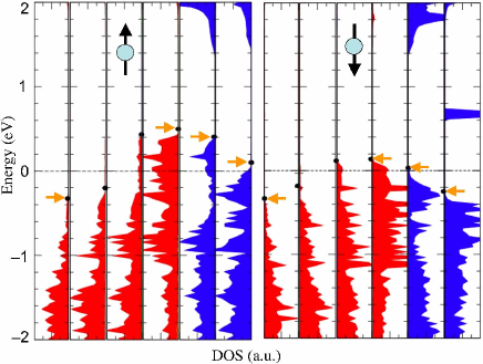
To calculate the band offset at the YMnO3/GaN interface, we project the spin-resolved DOS of the supercell onto unit cells of YMnO3 and bilayers of the GaN as shown in Fig. 4, and calculated the band offsets for both the spin-up and spin-down components. In the case of , the valence band offset (VBO) is eV for the spin-up component and eV for the spin-down component at interface , whereas a VBO is eV for the spin-up and eV for the spin-down at interface (“” and “” represent upward and downward offsets going from GaN to YMnO3). The band offset at both interfaces shows spin dependence. In particular, the spin-up electrons experience a potential higher by 0.2 eV than the spin-down electrons across interface . This suggests that electrons of different spin directions experience different electrostatic scattering probabilities and that spin-dependent barriers can be produced in AFM multiferroic/semiconductor heterostructures. This effect is associated with spin splitting at the top of the valence bands. Recently, BiMnO3 tunnel barriers were shown to be potential spin filters in magnetic tunnel junctions.Gajek07p296 But FM multiferroics such as BiMnO3 are rare. Thus our observation of spin-dependent barriers in AFM multiferroic/semiconductor junctions might enable the use of a larger group of multiferroics with AFM orderings as spin filtering devices.
In the supercell (not shown), we find a VBO of eV for the spin-up and eV for the spin-down at interface , similar to that of . At interfaces , the VBO is eV for spin-up and eV for spin-down, slightly higher in amplitude than that of . It is noteworthy that the offset of the structure is reversed for up and down spins from that in at interface B, which suggests a possibility of controlling the spin scattering by a reversal of the ferroelectric polarization in YMnO3. A small energy difference of meV is found in bulk YMO3 when the spins are switched from the collinear to noncollinear in-plane configurations.Fiebig05p883 This is much less than the barrier differences we found between the up and down spins. Thus the magnetic anisotropy should not influence the spin-dependent effect we observe.
In conclusion, we report the details of the electronic structure of hexagonal YMnO3-GaN heterojunctions. We consider two inequivalent Ga-O terminated interfaces that can be found in YMnO3 films grown on (0001) and (000) oriented GaN substrates and two possible orientations of the YMnO3 polarization with respect to that of the GaN substrate. We find different band offsets for spin-up and spin-down components, with a larger variance at the (000) interface. The spin-dependent interface barriers suggest that these heterostructures may be applicable in spin filtering tunneling devices. Our results are relevant not only to YMnO films but also to other multiferroic thin films with coexisting antiferromagnetic and ferroelectric structures.
This work is supported by the Office of Naval Research under grant N000 14-06-1-0362 and Texas Advanced Computing Center.
References
- (1) R. Ramesh and N. A. Spaldin, Nature Materials, 6, 21 (2007).
- (2) W. Prellier, M. P. Singh, and P. Murugavel, J. Phys. Cond. Matt. 17, 803 (2005).
- (3) C.J. Fennie and K.M Rabe, Phys. Rev. B 72, 100103 (2005).
- (4) B. B. van Aken, T. T. M. Palstra, A. Filippetti, and N.A. Spaldin, Nature Materials 3, 164 (2004).
- (5) N. Fujimura, T. Ishida, T. Yoshimura, and T. Ito, Appl. Phys. Lett. 69, 1011 (1996).
- (6) N. Fujimura et al., J. Appl. Phys. 80, 7084 (1996).
- (7) T. Yoshimura, N. Fujimura, and T. Ito, Appl. Phys. Lett. 74, 414 (1998).
- (8) W.-C. Yi et al., Appl. Phys. Lett. 73, 903 (1998).
- (9) K.-R. Balasubramanian et al., Thin Solid Films 515, 1807 (2006).
- (10) Y. Chye et al., Appl. Phys. Lett. 88, 2903 (2006).
- (11) A. Posadas et al., Appl. Phys. Lett. 87, 1915 (2005).
- (12) We have performed the LDA+U calculations using the Vienna Ab initio Simulation Package (VASP) with projector augmented wave potentials, a cutoff energy of 500 eV, and a Monkhorst-Pack -centered -points mesh for the bulk and supercell calculations. The supercell DOS was generated with a denser mesh. The forces from ionic relaxation of the supercells are meV/Å.
- (13) J.-S. Kang et al., Phys. Rev. B 71, 092405 (2005).
- (14) J.E. Medvedeva et al., J. Phys. Cond. Matt. 12, 4947 (2000).
- (15) B.B. van Aken, A. Meetsma, and T.T. M. Palstra, Acta Crys. Sec. C 57, 230 (2001).
- (16) T.J. Zywietz, J. Neugebauer, and M. Scheffler, Appl. Phys. Lett. 74, 1695 (1999).
- (17) S. Chevtchenko et al., Appl. Phys. Lett. 88, 2104 (2006).
- (18) V. Fiorentini et al., Phys. Rev. B 60, 8849 (1999).
- (19) M. Gajek et al., Nature Materials 6, 296 (2007).
- (20) Fiebig et al., J. Mag. MAg. Mat. 290, 883 (2005).