Sub-Threshold Field Emission from Thin Silicon Membranes
Abstract
We report on strongly enhanced electron multiplication in thin silicon membranes.
The device is configured as a transmission-type membrane for electron multiplication.
A sub-threshold electric field applied on the emission side of the membrane
enhances the number of electrons emitted by two orders of magnitude.
This enhancement stems from field emitted electrons stimulated by the incident particles,
which suggests that stacks of silicon membranes can form ultra-sensitive electron multipliers.
∗Electronic mail: QIN1@WISC.EDU
pacs:
79.20.Hx, 79.70.+q, 73.30.+y, 82.45.Mp, 61.46.-w, 87.64.Ee,Particle detectors crucially rely on electron multiplication, such as the photo and electron amplifier tubes, cathode ray screens and micro channel plates bruining-54 . The multiplication is conventionally achieved by employing the so-called secondary electron emission (SEE) bruining-54 ; modinos-84 , where a primary electron (PE) strikes the surface of the detector and induces the emission of lower energy secondary electrons (SEs). The physics behind SEE is found in the various interaction pathways between the PEs and the solid, e.g., electron-nuclear collisions, electron-electron interactions, plasmon and phonon excitations egerton-86 ; see-review . To the emission of SEs usually only those contribute, which are excited above the vacuum energy level (). Consequently, the barrier for releasing secondary electrons is determined by the difference between the vacuum energy level and the Fermi level: , the work function. The actual figure of merit for detectors, e.g., electron multipliers, is the secondary electron yield (SEY), which predominantly relies on the detector material. Naturally, many efforts focus on achieving high SEY by developing new materials with a lower work function, such as most recently doped diamond auciello .
Furthermore, it has been known that the external electric field at the surface of a metal or a semiconductor can significantly modify the potential barrier and induce field emission (FE) of electrons modinos-84 . The studies on field-enhanced SEE can apparently be traced back to the discovery of the Malter effect in 1936 malter-36 . Follow-up experiments on SEE revealed variants of this field effect pensak-49 ; jacobs-51 . These experiments were conducted on bulk metallic substrates coated with a thin layer of oxide, where apparently the oxide layer is the key. It is this thin surface layer, which either (a) becomes positively charged to induce field emission from the underlying emitter and leads to long persistence times of SEE or (b) induces avalanches of electrons in the oxide layer.
Here we present detailed SEE measurements on how to dramatically enhance SEY in thin semiconductor membranes by the electric field. The field enables sub-threshold electron extraction, increasing the yield by two orders of magnitude. We probe this effect in a transmission-type configuration, where the back side of the membrane emitter is bombarded by a primary electron beam (e-beam). In addition, our technique now allows to probe electronic excitations at low energies, which are otherwise not accessible by conventional SEE.
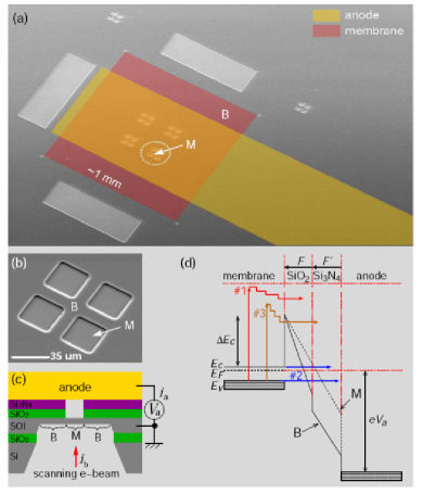
The device we realized is a thin silicon membrane which is capped with two thin layers of silicon oxide and silicon nitride. The starting material are silicon-on-insulator (SOI) wafers, which consist of a layer of silicon on a layer of silicon dioxide (). Both the SOI and silicon substrate have a crystal orientation of (100) and a resistivity of , corresponding to a n-type doping level of . The Fermi level is about below the bottom of the conduction band at room temperature. The SOI wafer was thinned by thermal oxidation to form a silicon dioxide layer (). The whole wafer is then capped with a thin layer of silicon nitride () by using low pressure chemical vapor deposition (LPCVD). A square () membrane of SOI/SiO2/Si3N4 triple layer is formed in an anisotropic silicon etching step using potassium hydroxide (KOH) solution.
Finally, 16 silicon membranes are formed from this triple-layer membrane by carving through the oxide and nitride layers. The scanning electron micrograph in Fig. 1(a) is a top view of the device, where the whole triple-layer membrane is seen as a red square and in the center are 16 silicon membranes. A closer view of four silicon membranes is shown in Fig. 1(b). Thus two distinct membrane types are fabricated on the same device: a pure silicon membrane (M) and a triple-layer membrane (B). Each M-type membrane has a dimension of , which is only of the area of the framing B-type membrane. The thickness of the M-type membranes is .
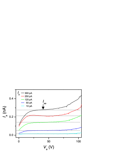
We used a modified SEM to conduct the experiments (vacuum of ): the configuration is sketched in the inset of Fig. 1(c), where the sample is clamped in a holder while the electron-beam is scanned over the backside of the membranes. The injected electrons possess energies in the range of . The membranes are connected to ground to avoid charging due to the release of electrons. A metallic anode is placed on top of the membrane, covering the gold-color area as shown in Fig. 1(a). This electrode provides the extraction or retarding voltage () for electrons emitted from the membranes. By controlling the anode voltage while monitoring the anode current , SEE () can be differentiated from electrons transmitted directly through the membrane (). As will be shown below, a further increase in the anode voltage induces FE from the membrane.
Energy band diagram of the membranes is schematically shown in Fig. 1(d). The existence of dielectric layers enhances the electric field at the surface of the SOI layer. The potential barrier for electron emission in area B is determined by the conduction band offset between silicon oxide and silicon (), while it is the work function () of silicon for area M. When the backside of the membrane is exposed to an electron-beam, SEE can be easily probed by the anode, as shown in Fig. 2. This is indicated by process #1 shown in the energy diagram in Fig. 1(d). Due to the thinness of the membrane which allows direct electron transmission, the anode draws already a finite current even at a negative bias bruining-54 ; qin-07 . The increase of up to allows for a complete collection of both transmitted and true SEs, which produces a plateau in the curve, as shown in Fig. 2. The height of this plateau normalized by the incident beam current defines the conventional electron yield from SEE: , which is found to be about .
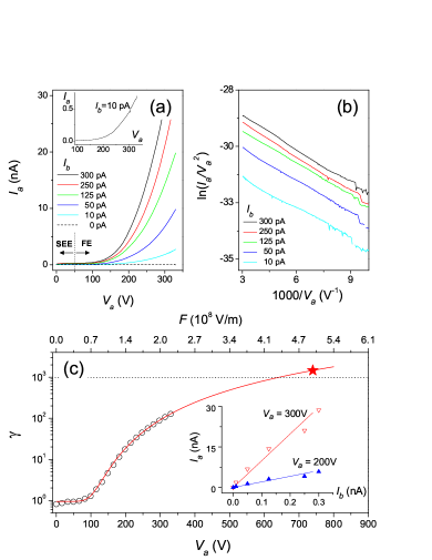
Without electron-beam excitation on the backside of the membranes, electrons in the conduction and valence bands can be emitted through FE, shown as process #2 in Fig. 1(d). Without injected electrons our device did not show a measurable FE current, even when an anode voltage of up to is applied, see the black dashed curve shown in Fig. 3(a). This is not too surprising since at , the electric fields in area B and M are only of the order of . According to the Fowler-Nordheim (FN) theory, such sub-threshold electric fields do not produce a detectable electric current from an emission area of . However, when the backside of the membrane with an area about including 16 M-type membranes is exposed to an electron-beam, the anode current is significantly increased, as shown in Fig. 3(a). The electron-beam has an energy of and a beam current as indicated. A similar nonlinear curve is also seen in the inset of Fig. 3(a), where the electron-beam is fixed on a M-type membrane, i.e. without any dielectric layer. This suggests an emission mechanism different from the Malter effect malter-36 and the other known effects pensak-49 ; jacobs-51 which all rely on a thin layer of oxide deposited on the emitter.
The observed strong electron emission with above is further examined along the FN characteristic: , as shown in Fig. 3(b). The straight lines in a large range of bias voltage strongly support that emission from the membranes is governed by FN tunneling: , where stands for the conventional SEE which saturates around (see Fig. 2), while the second term is the standard FN field emission current ( and are material dependent constants with ). Most importantly, we found that coefficient is proportional to the incident electron-beam intensity: .
The total yield can now be expressed as , which can be continuously tuned by the anode voltage. As shown in Fig. 3(c), a yield of 200 is achieved by strong FE at a bias of . Below , the yield is reduced to which is determined by conventional SEE. The solid curve shown in Fig. 3(c) is a fit with and , which traces perfectly. In the inset of Fig. 3(c) plots are represented for constant yields. Here we fixed the anode voltage and varied the electron-beam current ().
The above results reveal that electrons in a thin silicon membrane can be generated and liberated by the combined action of PEs and an external electric field. In other words, the external sub-threshold electric field induces field emission of those electrons excited by the primaries, which would otherwise remain undetected. Unlike the Malter effect, a dielectric layer on the surface of the membrane is not a must in our experiments and no self-sustained emission was observed after the scanning electron-beam is turned off beamsize .
The main pathway for this sub-threshold field emission which we found here, is illustrated as process #3 shown in the band structures of Fig. 1(d). the corresponding portion of the emission current should follow , where is the number of electrons excited to the energy between and , is the tunneling probability. The spectrum of possible electron excitations in the thin silicon membrane by the PEs should be a continuum, starting from the bottom of the conduction band to the energy level of PEs. Electrons at the membrane surface with an energy above the tunnel barrier are true SEs since they are free to escape from the membrane. However, there are many more electrons excited with their energy below the barrier. Especially, for electrons with an energy close to the top of the barrier will have a tunneling probability as high as .
Following this model, a yield as high as 1000 could be realized at or equivalently , which is still below the dielectric breakdown voltage of silicon dioxide (, marked by in Fig. 3(c)). Importantly, such a (flat) membrane as an emitter covered with silicon oxide will not sustain a high electric field suitable for intrinsic field emission (processes #2 in Fig. 1(d)) without triggering a dielectric breakdown in the oxide layer. By introducing nanopillars as electron emitters onto thin membranes, we would be able to achieve an even higher yield and observe a transition from stimulated sub-threshold FE to intrinsic FE qin-07 ; kim-07 .
Apart from applications in transmission-type electron multipliers wilock-60 , this effect also allows for determination of the excitation spectrum, such as, phonons and plasmons, both of which have an energy below the tunnel barrier and are not detectable by conventional SEE. Electron emission assisted by these quasiparticles is essential for developing particle/radiation detectors with an ultra-high sensitivity and low dark current.
In conclusion we have demonstrated enhancement of electron multiplication of at least two orders of magnitude in a silicon membrane device. The experimental results suggest that this field-dependent multiplication does not require a dielectric layer on the membrane as found in Malter’s experiment. The multiplication is simply realized by sub-threshold Fowler-Nordheim field emission. The device architecture demonstrated allows for an easy realization of stacked electron and other particle detectors and for probing electronic, photonic, or phononic excitations of thin semiconductor membranes.
We like to thank the Wisconsin Alumni Research Foundation for direct support of this work and the National Science Foundation for partial support (MRSEC-IRG1).
References
- (1) H. Bruining, Physics and applications of secondary electron emission, McGraw-Hill Book Co. Inc. New York (1954).
- (2) A. Modinos, Field, Thermionic, and Secondary Electron Emission Spectroscopy, Plenum, New York, (1984).
- (3) R. F. Egerton, Electron energy loss spectroscopy in the electron microscope, Plenum Press, New York (1986).
- (4) R. Shimizu and Z. -J. Ding, Rep. Prog. Phys. 55, 487 (1992).
- (5) S. Srinivasan, J. Hiller, B. Kabius, and O. Auciello, Appl. Phys. Lett. 90, 134101 (2007).
- (6) L. Malter, Phys. Rev. 50, 48 (1936).
- (7) L. Pensak, Phys. Rev. 75, 472 (1949).
- (8) H. Jacobs, Phys. Rev. 84, 877 (1951).
- (9) It has to be noted that the electron yield was found to be independent of the spot size of the electron-beam. At , an electron-beam of and a spot size of inject single electrons one by one into the membrane. This suggests that the observed electron multiplication stems from the interaction between individual PEs and the thin membrane.
- (10) H. Qin, H. S. Kim, and R. H. Blick, http://xxx.lanl.gov/0708.2470.
- (11) H.S. Kim, H. Qin, and R.H. Blick, Nanotechnology 18, 065201 (2007).
- (12) W. L. Wilcock, D. L. Emberson, and B. Weekley, Nature 185, 370 (1960).