Negative differential resistance of Styrene on an ideal Si[111] surface: dependence of the I-V characteristics on geometry, surface doping and shape of the STM-tip
Abstract
We study the electron transport properties through a supported organic molecule styrene (C8H8) on an ideal silicon surface Si[111] and probed by a STM-tip. The I-V characteristics and the differential conductance of the molecule are calculated using a self consistent approach based on non equilibrium Green’s functions. Two different adsorption configurations for the molecule on the surface were considered which corresponds to a global and a local minimum of the total energy. In both cases we find a negative differential resistance (NDR) in a given interval of bias voltages. This effect is controlled by the states available close to the Fermi level of the surface and can be manipulated by properly doping the substrate. We also analyze the influence of the tip-shape on the I-V characteristics.
pacs:
73.63.-b,73.22.-f,73.40.GkI Introduction
Transport properties through supported molecules on substrates
are an interesting phenomena in the field of nanodispositives.
This idea has been
extensively studied in the last few years mainly due to the possibility to
build electronic dispositives at atomic scale.
The major bottle neck in nanoelectronics is to have different mechanisms to control
the transport properties as wish. In order to get to this point
experiments and theory should work together by investigating different
molecules, substrates and physical properties to achieve this goal.
In the case of substrates, two different approaches have been followed
by using metallic or semiconductor surfaces as the electrodes which
interact with a given molecule.
With metallic contacts, the conduction could be described
through an ohmic behavior, but if non-metallic contacts are considered
(where the surface can have gaps in the electronic dispersion relation
or if the molecule and surface
interaction is able to open a gap), the electronic transport could
change. Changing the molecule type has been also further
investigated and many interesting results could be found in the literature.
Some examples about electronic transport in mesoscopic systems consider
carbon nanotubes used as nanowires Tans et al. (1997), metal-ion clusters useful
for information storage Sessoli et al. (1993) and
molecules such as small silicon clusters that
have been then studied showing resonant
tunneling effects due to the electronic states of the cluster Bolotov et al. (2001).
In the particular the case of silicon clusters in contact with semiconductor
surface have been theoretically investigated in our group. We did report
a diode-like behavior, opening the possibility of using a like dispositive in the
the design of new electronic dispositives Baltazar et al. (2007).
Channels responsible of the electronic
flow are not only established by the molecular levels of the molecule,
but also by the position of the Fermi level associated with the surface.
Recently, negative differential resistance (NDR) on heavily
doped Si substrates in contact with organic molecules
has been predicted theoretically Rakshit et al. (2004) and demonstrated
experimentally Guisinger et al. (2004). This observation has been related to the
crossing of the HOMO or LUMO levels of the band edge of the underlying
semiconductor. It has been also pointed out that by using different molecules such as
metallic nanocrystals or organic molecules, the conductance can be changed to be
diode-like behavior and showing a dependence on the used molecules
Reed et al. (1997); Klein et al. (1996). These recent results have reinforced the idea
of using molecular systems as active structures in electronic components
at nano scale.
In this work, we want to consider the electronic transport through an organic molecule
in contact with a
semiconductor surface. We report and explain a non-ohmic behavior in the electronic
transport and we relate this observation to the
interaction between the different systems. Transport properties are also tested under
different conditions, such as doping and applied external electric fields.
II Formalism
In this section we draw the methodology we have followed to calculate the
transport properties here reported. This methodology has been previously
presented by De Menech to study silver clusters and C60 fullerenes
on metal surfaceset al. De Menech
et al. (2006a, b).
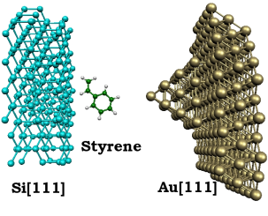
Our system consists of substrate-molecule-electrode. The surface has
been modeled as an ideal structure with no reconstruction after the
molecule has been absorbed on it. The electrode is a metallic tip far away
from the molecule, with no bonding with it. The
transport properties at equilibrium and non-equilibrium conditions
were calculated using a Green’s functions approach. The electronic states are
described by means of a semiempirical extended Hückel
theory (EHT), where parameters are obtained from first principle
calculationsCerda and Soria (2000). We did guarantee a very good agreement between
our electronic description and ab initio calculations, with errors less than 2%
around the Fermi energy.
From the Hamiltonian of a molecule and a contact ,
a coupled system (contact - molecule) can be described by
the composite Schrodinger equation
| (1) |
where S is the normalization matrix and is the Green’s function of the total system. By using the Green’s function, the spectral function (density of states per unit energy) can be written as
| (2) |
for the spin unpolarized case. Following this description, the local density of states can be written as
| (3) |
where s are the molecular wavefunctions, giving rise to the electronic density as
| (4) |
that considers the integration just until the Fermi energy level.
Now, if we want to study the consequences on a specific part of the system due to the presence of the other parts, the Green’s function approach allows it by including the effect as perturbations on the original Green function. This approach has been described by Williams et al. Williams et al. (1982) to study defects in crystals as perturbations. They have showed that the problem can be described by a Dyson equation and have obtained the Green’s function of the perturbed system. In our case, the Dyson equation leads to the perturbed Green’s function of the cluster due to the presence of the surface. The surface effects are included as
| (5) |
where and are the Green’s functions associated with the isolated (unperturbed part) and the supported cluster (perturbed) respectively, and is the self-energy matrix given by:
| (6) |
The previous equation takes into account the effect of the surface, which could come as broadening and shifting of molecular energy levels (the size of , and are defined mainly from the molecular orbitals values). The term corresponds to the Green’s function of the isolated surface and is the coupling matrix between the cluster and the surface. The non equilibrium regime, is considered when another electrode is added to the system and an external voltage is applied between the surface and the electrode. In this case, the representation for the supported cluster is changed by using the correlation function to determine the charge density at a specific bias . The term is the lesser self-energy that depends on the Fermi function of the contact (surface and electrode) for a specific chemical potential and the broadening matrix of the surface and the metallic electrode. The rate at which electrons goes from one contact to another through the cluster is the transmittance . By considering only coherent transport (no scattering), it is possible to show that can be evaluated using the relation
| (7) |
Finally, the expression used to calculate the current through a system like the one depicted in fig. 1, where a molecule, with discrete energy levels, is located between a semiconductor surface and an electrode (with a uniform distribution of states), can be written as
| (8) |
The transmittance is integrated in the energy interval associated
with each applied bias voltage and restricted by the
Fermi function of the contacts.
For both cases
(surface and electrode), local equilibrium is assumed and, in principle,
the low temperatures approximation is used, so the integration can be
performed between and .
After the calculation of the transmittance is performed, we did follow the treatment given by Tian et al. Tian et al. (1998) to obtain the conductance and the differential conductance. At low temperature regime, the conductance will be proportional to the transmittance (at zero bias), where the differential conductance will be written as
| (9) |
where is the maximum conductance constant.
Here it is assumed that the electrostatic potential modifies mostly the
chemical
potential of the metallic electrode. To describe the molecular electronic
properties we use the EHT approach, where the electronic Hamiltonian is parameterized
through the matrix elements , between
two atomic orbitals and of atoms and respectively
and assumed to be proportional to the overlap
and such that
.
According with Cerda et al. Cerda and Soria (2000), the parameter
can be defined from the on site energies using the form:
, where
is a fitting parameter usually obtained for solids and calculated
from first principles.In our case this value was fixed at 1.75 for H, 2.8
for C and 2.3 for Au and Si.
In order to evaluate the accuracy of this model, we have compared the description
obtained with the EHT model, with a calculation based on a plane wave implementation
of the density functional theory with normalized pseudo potentials,
as implemented in CPMD © IBM Corp. 1990-2001 (1990).
The exchange-correlation has been described by using the
local spin density approximation (LSDA) Lee et al. (1988); Becke (1988).
The atomic structure and energy minimization
of the isolated molecule and the
supported molecule in contact with the surface have been calculated
at the same theory level.
III Results
In order to make a proper electronic characterization of the system, we did start by describing every one of the system components as isolated systems. The surface considered in this work is a semiconductor silicon with a [111] orientation and no reconstruction. Even though, it is experimentally more typical to find this surface as reconstructed in (2x1) and (7x7), depending on temperature Watanabe et al. (1998); Bolotov et al. (2001), it has been also possible to obtain a Si[111]- in a (1x1) surface reconstruction Khan (1983). For the unreconstructed surface, the dangling bonds are associated to the discrete energy levels that can be observed at the band structure of the Si[111] surface. In the case of the molecule, we have selected styrene (C8H8) as the organic molecule in contact with the surface. This molecule has been previously considered and experimentally studied as a possible component in the design of new molecular devices Guisinger et al. (2004). For the coupled case, the interaction between the organic molecule and the Si[111] surface has been obtained from a geometrical optimization from first principle calculations. The final atomic structure feed to the transport calculation is the lowest energy geometry. The structural optimization has been obtained considering the local spin density approximation (LSDA) as the exchange and correlation terms S.Goedecker (1996). From the optimization, we have obtained two possible structural configurations for the supported molecule, labeled as case A and B from now and on. The optimization also defines the optimal distance between the molecule and the surface. The energy difference between both configurations is 15.8 eV, being case B the most stable. This result was calculated using a computational package Gaussian 98 et al. (1998)
III.1 C8H8 on Si[111] : (case A)
For the case named as A, the energy difference between the HOMO and LUMO levels of the free molecule is 0.95 eV. Whereas, in the coupled case, the electronic gap is obviously reduced and the optimal molecule-surface distance is found to be 2.5 angs. By using the minimal structure, the electronic structure is calculated using the EHT model (as previously discussed). A fair comparison with the electronic levels from ab-initio calculations was found. between them.
In order to evaluate equilibrium properties we have considered
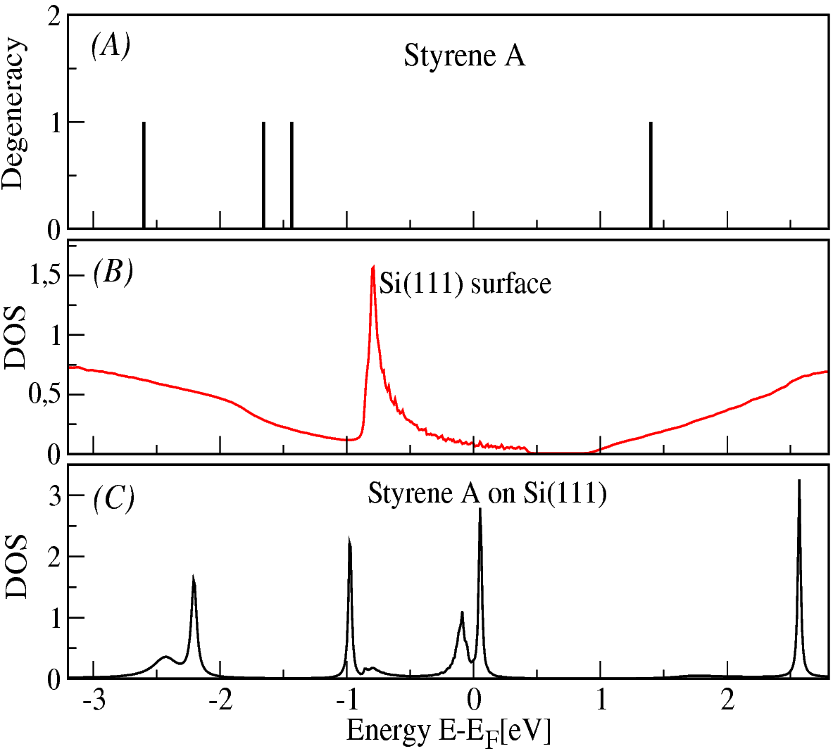
Figure 2 that shows the electronic density of states of the
system calculated within the EHT approach. In Fig. 2-A the
electronic levels of the free molecule are presented.
In Fig. 2-B, the e-DOS of the Si[111] surface is shown. An
electronic gap of 0.45 is
observed and dangling bonds are located around 0.7 eV below the Fermi
level. This description is in good agreement with results reported by
Pandey Pandey and Phillips (1976) and Schlüter Schlter
et al. (1975),
obtained using a semiempirical tight-binding method and a self-consistent
pseudopotential respectively. The presence of the dangling bonds is observed in
these cases with a shift of the states compared with our results and given
because of the parameterization of the considered model.
Finally, in Fig. 2-C the e-DOS of the molecule interacting with
the surface is shown. The energy levels of the free cluster are broadened and
red shifted (moved to the right side)
in the coupled case
As a consequence, there are more states close to
the Fermi level and the gap of the surface.
Once we have established the equilibrium conditions,
a metallic electrode is included in the system to evaluate transport
properties. As a first approach,
an ideal Au(111) surface is considered as an electrode. Initially,
the electrode and surface are initially at local equilibrium and with chemical
potentials =-5.26 eV and =-4.8 eV
respectively Allen and Gobeli (1962).
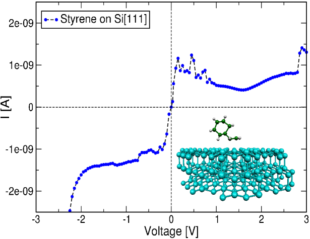
Under non-equilibrium conditions, an external bias is imposed by changing the chemical potential of the metallic electrode. Then the transmittance T(E,V) is calculated and the current can be obtained integrating the transmittance in the energy range associated to each bias. I-V curve is shown in Fig. 3 where the applied bias goes from -3 to 3 V. We can observe a NDR effect for a positive applied bias. The intensity of the current starts to decrease at 0.7 V finding a minimum around 1.5 V where the current starts to increase again. This effect has been also experimentally reported for styrene on Si[100] Guisinger et al. (2004). In this case, we have evaluated the states close to the Fermi level finding a shifting effect (adjustment of the position of molecular levels) as a function of the applied bias in the DOS and a drop in the transmittance when the bias is larger than 0.5 V. The molecular state, located next to the Fermi level (see Fig. 2-C ), will be crucial when we have to explain the major contribution to the NDR effect. This state is the main peak in the DOS located in the right side of the DOS respect to the Fermi level (that in this case was considered at -4.8 eV for Si[111]) and the charge distribution associated to it is located mainly between the molecule and the silicon surface. In Fig. 4 the DOS of the styrene molecule is compared with the differential conductance dI/dV as a function of bias.
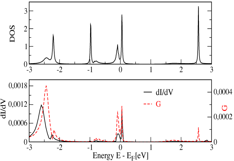
In the case
of dI/dV, we can see not just the shift of the peaks respect to the e-DOS but
also the magnitude of some peaks clearly changing, when they are
compared to other peaks also observed in the e-DOS.
The dI/dV characteristic in Figure 4 shows the molecular states
that indeed contribute to the electronic transport in the system.
In this context, the intensity of the two peaks located at +/- 0.2 eV
respect to the Fermi level are clearly defined, in contrast to the state
located 1 eV below the Fermi level.
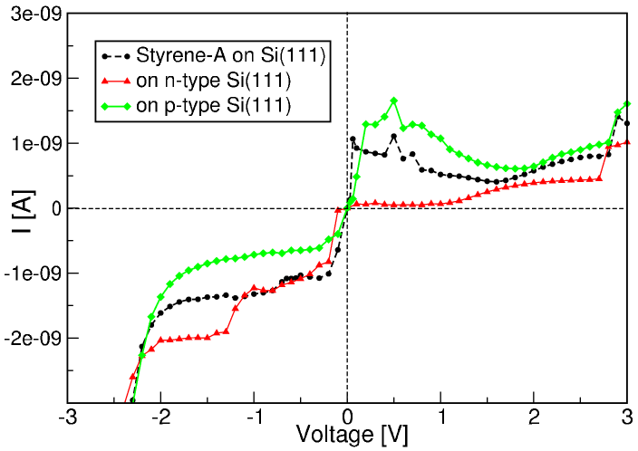
Another parameter we did take into account is related to the doping on the surface.
To consider doped surfaces, a simple approximation can be performed without the
inclusion of atoms in the system, such as P or S. This can be achieved by
modifying the Fermi level of the
substrate. We have considered three cases where the chemical potential of the
surface is assumed to be -4.8 eV (initial case), -4.3 eV (n-type) and
-5.3 eV (p-type). For each case, there are different equilibrium conditions
controlled by the chemical potential.
We have calculated the transmittance in the
system and then the current . These results have been depicted in
Fig. 5 where a voltage range from -3 to 3 V has been used. In this figure we can see
that the n-type surface shows a similar behavior compared to the non-doped
case (), where the NDR effect at positive bias is observed.
In the case of the p-type
surface the result is rather different. The NDR is not found at positive bias and
even the behavior at negative is also different when it is compared with
the previous cases.
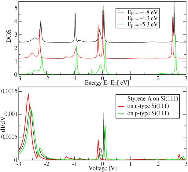
In order to understand the differences at each doped o undoped surface Fig. 6 shows the e-DOS and the differential conductance dI/dV. Even considering that the peaks of e-DOS are clearly shown at each case, we can see a displacement of the peaks as well as a change in their magnitude. In the case of dI/dV, the peaks are again shifted and changed in magnitude. One of the important aspect of the doping effect, is that molecular states have been also shifted according to each doped case and, in particular, the n-type surface () have moved (red shifted) the molecular states to the region of the calculated energy gap for the Si[111] surface (see Fig. 2).
In order to differentiate the influence of the tip geometry, we did consider two different geometries: a flat surface and a pyramidal structure. The last geometry is shown in Fig. 7 where the tip shape is obtained with 30 Au atoms. The molecule-tip distance has been fixed to 5.0 angs. For the flat electrode, we have considered a distance of 5.2 angs. These distances are long enough to consider only tunneling current between the molecule and the tip/electrode.
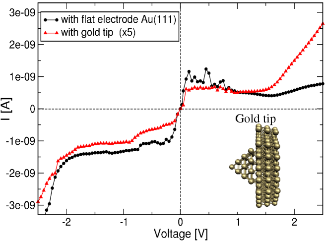
Fig. 7 shows the I-V characteristics with and without a tip. In the case of the tip, the intensity of the current was multiplied by 5 for better comparison. We can see that at low voltages (positive and negative), the behavior is rather similar between them, but this description changes when the bias is higher in the positive direction. The NDR effect observed in the case of the flat electrode, has been diminished until dissappear, showing in contrast an almost constant behavior when a bias between 0.5 and 1.5 V is applied.
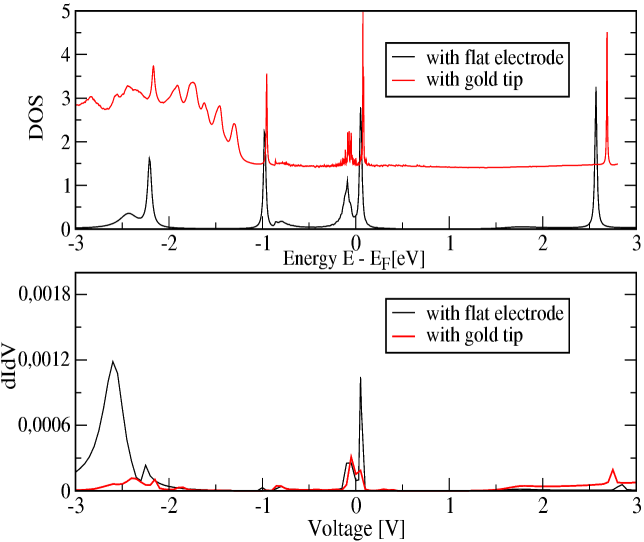
The calculated e-DOS and the dI/dV in Fig. 8 show the comparison
between the flat electrode and the tip,
in particular, a change in the magnitude of the peak located at 0.2 eV above the Fermi
level, where the intensity is diminished when the tip is considered.
There is also another difference mainly localized at lower
energies and can be attributed to the considered tip.
III.2 C8H8 on Si[111]: B case
The previous discussed molecular geometry is the one which has attracted more attention when it is supported by Si[100] surface Guisinger et al. (2004). Nevertheless, We have found a second, stable configuration (B case) when the styrene molecule is interacting with the Si[111] with no reconstruction. Is important to notice that the energetic optimization shows that E(case B) E(case A), which means that this configuration is much more stable. In this case, the optimal distance between the molecule (H atoms) and the surface (Si atoms) was found at 2.8 angs.
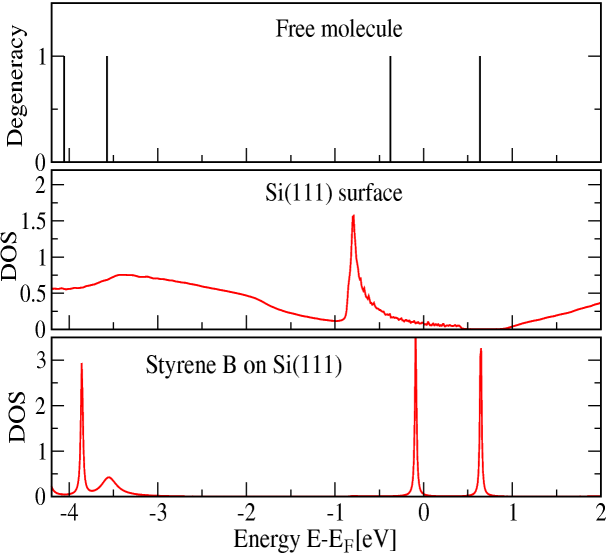
Figure 9 shows that energy levels associated with the case B free molecule (graph A) and the e-DOS of the Si[111] surface (graph B) and the molecular levels for the molecule interacting with the surface (graph C). From the e-DOS of the supported molecule, we can see molecular levels energetically located not only close, but also in the energy gap associated to the surface (graph B in Fig. 9). The two molecular states localized around 0 and 0.7 correspond to the original LUMO and LUMO+1 states respectively and they play an important role in the conduction phenomena. After we have evaluated the electronic configuration at equilibrium conditions (without bias), the I-V curve is shown in Fig. 10 with the same voltage range as case A. Interestingly, the I-V characteristic does not seem to show a similar NDR effect when a positive bias is applied, like in the first case. Instead of this effect, there is no an important contribution for the current at low positive voltages until a bias of 2.0 V is applied. Instead, when the negative bias is considered, there is current flow even at low voltages.
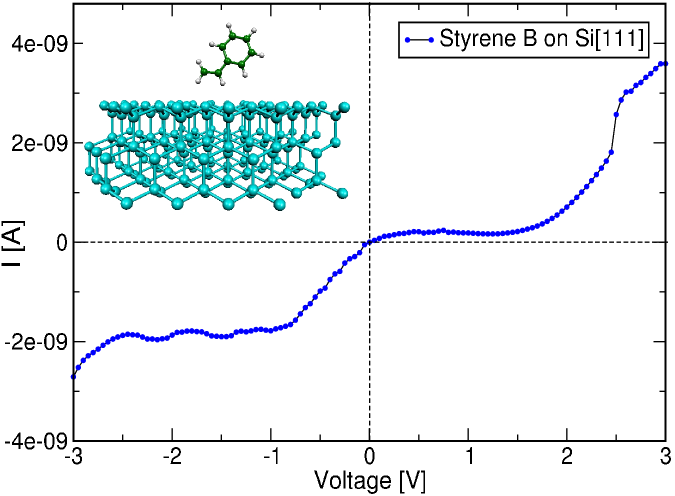
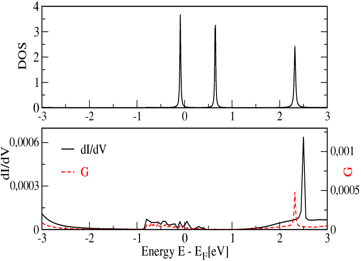
If we want to know about the states that participate in the electronic transport, it is possible to evaluate the differential conductance dI/dV and the conductance in Fig. 11. In this case, the contribution of the state located initially at 0.7 eV above the Fermi level, has a very small intensity in dI/dV characteristic compared to other states. Even the conductance and the dI/dV of the state located at 0.2 eV below the Fermi level, is also small in comparison to, for example, the states located at 2.3 eV above the Fermi level. There is also a spread distribution of the conductance and dI/dV characteristics for low negative values (between -1.0 and 0.2 eV below ). In this case, there will be important to notice that this distribution is located in the same energy interval associated to the dangling bonds on the silicon surface.
Following the same lines than in the previous configuration, we did also study the transport properties as function of surface doping. As previously explained, we did obtain these conditions by modifying the chemical potential. Results for the I-V characteristics are shown in Fig. 12. This figure shows clearly different results when the substrate is n-type or p-type doped. In the first case, we have the results obtained for C8H8 (B case) on Si[111] with a chemical potential of -4.8 eV (original conditions). The current increases steadily after an applied bias of 2.0 V. When the surface is n-type doped (considering ), there is no response in the current until 0.6 V, where the intensity starts to increase rapidly with the positive applied bias. A completely different behavior is obtained when the surface is p-type (which means that ). Here we can see that a NDR effect is obtained for the current around 1-2 V, when even if the positive bias is increasing, the current flow is decreasing in magnitude until a minimum value around 2 V. After this bias, the current increases its value again in a similar way like in the two other doped surfaces.
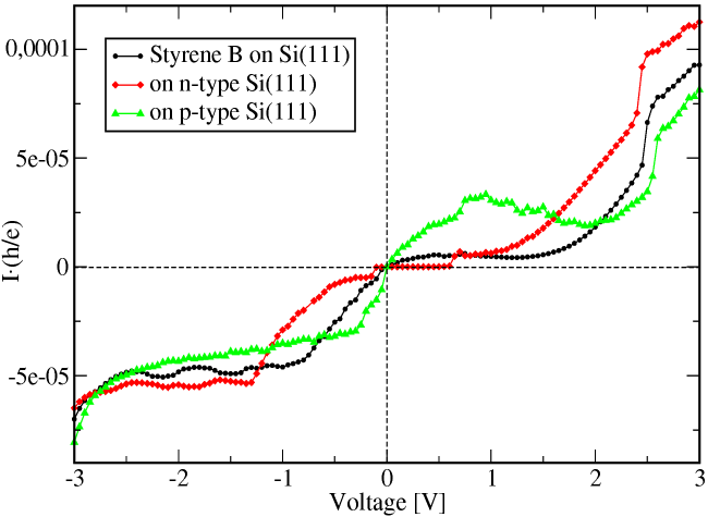
The figure 13 shows the DOS and the dI/dV characteristic associated with doped o undoped surface. Here, we notice that the energy has been adjusted to each different Fermi level, so the zero energy position is indeed different for each condition. It is important to notice that even with a similar distribution of the molecular states, the differential conductance looks rather different. For the undoped surface, there is no an important peak for dI/dV at low voltages and the main one is located at 2.4 V, with a spread contribution of states obtained around 0 V. If we consider the n-type Si[111] surface, we can detect an important peak located around 0 V within with the same spread distribution as for the undoped case. For the p-type surface, we can see a small peak around 0.0 V and 2 important peaks, one located around 0.7 V and the other one at 2.5 V.
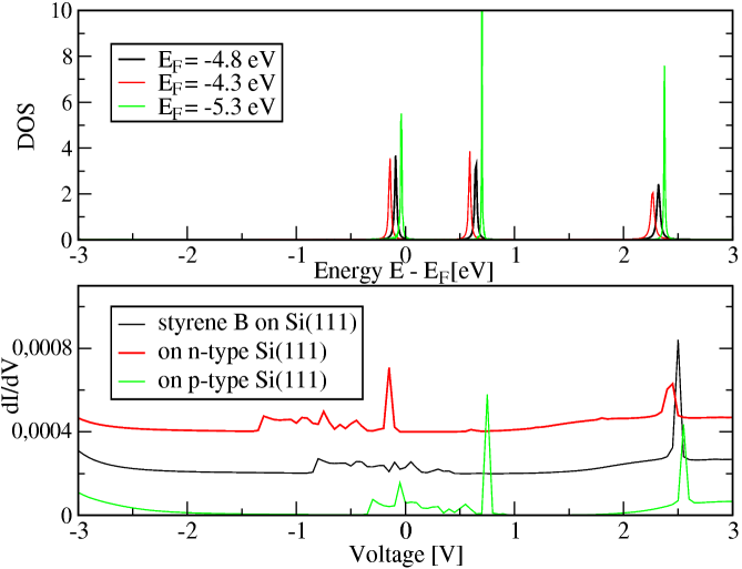
For all doped-undoped surfaces, the same peak, locate around 2.5, is clearly depicted and is related to the state found at 2.4 eV above the Fermi level. Again, the states related to the peaks close to the Fermi level, provide the most important contribution when a low voltage regime is considered.
IV Discussion and conclusions
Here, we have reported a set of electronic transport calculations for a
semiconductor-cluster-electrode system. Initially we have obtained two
possible configurations (A and B cases) for the styrene molecule
given by the minimization of the
energy associated to the surface-molecule system . The most stable configuration corresponds
to the B case and the A case corresponds to the atomic configuration of the
molecule used for Si[111] surface, as it is shown in Fig. 3.
For the A case, we have obtained a NDR effect when a
positive bias is applied. This can be understood based on the shifting of the
molecular levels, close to the Fermi level, when the voltage is applied.
This effect is modulated when the surface has been doped, which changes the chemical
potential. This effect is more important
for the case of a p-type surface, as it is observed in Fig. 3, when
compared to the n-type surface, where the effect
is eliminated from the I-V characteristic. This difference is
achieved because of the shift of the molecular levels according to each doped surface.
For the n-type surface (with =-4.8 eV), the electronic molecular levels are
energetically located inside the energy gap of the silicon surface, so
there is no channel available for the electronic transport at low positive bias
(see dI/dV curve for n-type surface in Fig. 6). Another result,
shows the influence of the tip in the electronic transport, where if the tip
is changed, the NDR effect could be diminished with respect to the flat electrode.
In order to compare both conditions, we have used a similar
molecule-tip/electrode distance (5 angs.).
This can be understood from the potential created by the tip-surface, which is
smaller than the potential created by the electrode-surface case. A smaller
electric field created for a sharp tip promotes a very small shift of the
energy levels of the molecule and then it is more difficult to move the
states to the energy interval associated to the energy gap of Si[111].
For the second configuration (B case), the situation is rather different
because there is no NDR when the undoped surface is considered. This can be concluded
by observing that the main peak occurs at 0.7 eV above and therefore
can not be used as an electronic channel due to the energy gap of the Si[111].
Also, to control the NDR effect, we have considered doped surfaces,
where it is possible to detect the NDR effect for the p-type surface but not for
the n-type case. This difference is explained because the number of the channels
available, and close to the Fermi level, is lesser for the undoped surface than for
the p-type surface. Then the shifting of the
states produced by
the applied bias diminishes the contribution of the peak that is energetically
displaced to the energy gap of the doped surface.
In Fig. 13, we can see that the undoped surface
and the n-type case do not show important peaks close to the Fermi level
in the dI/dV characteristics and the most important contribution comes from
the state located 2.3 eV above . If we consider the p-type surface,
we can see not only the contribution given by the states related to the
dangling bonds of the surface around the Fermi level, but also one peak
located at 0.7 eV above and another one at 2.5 eV above .
In summary, the extended Hckel model, used to describe the electronic properties in the system, it is in good agreement when compared with ab initio calculations. We have found two stable configurations for the styrene molecule in contact with the surface and both of them can provide interesting properties like the NDR effect. This effect is modulated not only by the electronic molecular levels but also their positions respect to the energy gap of the silicon surface. A semiconductor surface has interesting properties respect to metallic ones, allowing to control transport with the appropriate conditions like doping. In our case, we have a NDR effect of the system at low positive voltage. This effect is also more important when a strong electric field has been considered to shift the molecular states (flat electrode produces a stronger electric field than a sharp tip). The comparison between flat and sharp electrodes has been performed for both configurations finding the same NDR suppression when a sharp metallic tip is considered. These results strength the idea to use organic molecules as possible components to storage information in electronic devices.
M. E. G. acknowledges the kind hospitality at the IPICYT. This work has been supported by the DFG through the SPP1153. A.H.R. also thanks the support of Conacyt Mexico under the grant J-46247-F. S. E. B. acknowledges the scholarship given by IPICyT and the University of Kassel.
References
- Tans et al. (1997) S. J. Tans, M. H. Devoret, H. Dai, A. Thess, R. E. Smalley, L. J. Geerligs, and C. Dekker, Nature 386, 474 (1997).
- Sessoli et al. (1993) R. Sessoli, D. Gatteschi, A. Caneschi, and M. A. Novak, Nature 365, 141 (1993).
- Bolotov et al. (2001) L. Bolotov, N. Uchida, and T. Kanayama, Eur. Phys. J. D 16, 271 (2001).
- Baltazar et al. (2007) S. E. Baltazar, M. D. Menech, Saalmann, A. H. Romero, and M. E. Garcia, submitted to J. Appl. Phys. (2007).
- Rakshit et al. (2004) T. Rakshit, G.-C. Liang, A. W. Ghosh, and S. Datta, Nano Letters 4, 1803 (2004).
- Guisinger et al. (2004) N. P. Guisinger, M. E. Greene, R. Basu, A. S. Baluch, and M. C. Hersam, Nano Letters 4, 55 (2004).
- Reed et al. (1997) M. A. Reed, C. Zhou, C. J. Muller, T. P. Burgin, and J. M. Tour, Science 278, 252 (1997).
- Klein et al. (1996) D. L. Klein, P. L. McEuen, J. E. B. Katari, R. Roth, and A. P. Alivisatos, Appl. Phys. Lett. 68, 2574 (1996).
- De Menech et al. (2006a) M. De Menech, U. Saalmann, and M. E. Garcia, Appl. Phys. A 82, 113 (2006a).
- De Menech et al. (2006b) M. De Menech, U. Saalmann, and M. E. Garcia, Phys. Rev. B 73, 155407 (2006b).
- Cerda and Soria (2000) J. Cerda and F. Soria, Phys. Rev. B 61, 7965 (2000).
- Williams et al. (1982) A. R. Williams, P. J. Feibelman, and N. D. Lang, Phys. Rev. B 26, 5433 (1982).
- Tian et al. (1998) W. Tian, S. Datta, S. Hong, R. Reifenberger, J. I. Henderson, and C. P. Kubiak, J. Chem. Phys. 109, 2874 (1998).
- © IBM Corp. 1990-2001 (1990) Computer code CPMD version 3.9.2, ©IBM Corp., 1990-2001 and ©MPI für Festkoerperforschung Stuttgart, 1990-2001.
- Lee et al. (1988) C. Lee, W. Yang, and R. Parr, Phys. Rev. B 37, 785 (1988).
- Becke (1988) A. D. Becke, Phys. Rev. A 38, 3098 (1988).
- Watanabe et al. (1998) M. O. Watanabe, T. Miyazaki, and T. Kanayama, Phys. Rev. Lett. 81, 5362 (1998).
- Khan (1983) A. Khan, Surf. Sci. Rep. 3, 193 (1983).
- S.Goedecker (1996) M. S. Goedecker, J.Hutter, Phys. Rev. B 54, 1703 (1996).
- et al. (1998) M. J. Frisch et al., Computer Code GAUSSIAN 98, Gaussian, Inc., Pittsburgh, PA, USA (1998). http://www.gaussian.com
- Pandey and Phillips (1976) K. C. Pandey and J. C. Phillips, Phys. Rev. B 13, 750 (1976).
- Schlter et al. (1975) M. Schlter, J. R. Chelikowsky, S. G. Louie, and M. L. Cohen, Phys. Rev. B 12, 4200 (1975).
- Allen and Gobeli (1962) F. G. Allen and G. W. Gobeli, Phys. Rev. 127, 150 (1962).