Scale dependent superconductor-insulator transition
Abstract
We study the disorder driven superconductor to insulator transition in amorphous films of high carrier-concentration indium-oxide. Using thin films with various sizes and aspect ratios we show that the ‘critical’ sheet-resistance depends systematically on sample geometry; superconductivity disappears when exceeds k in large samples. On the other hand, wide and sufficiently short samples of the same batch exhibit superconductivity (judged by conductivity versus temperature) up to which is considerably larger. These results support the inhomogeneous scenario for the superconductor-insulator transition.
pacs:
74.20.Mn 64.60.AkI Introduction
Sufficiently strong spatial disorder may precipitate an insulating phase in an otherwise metallic system. When the ground state of the metal under study is a superconductor, the disorder-driven transition is called the superconductor to insulator transition (SIT). The SIT has been studied over many decades, especially in thin films where tuning the disorder is readily achieved by varying the film thickness 1 ; 2 ; 3 ; 4 ; 5 ; 6 ; 7 ; 8 . Many common features of the SIT in such 2D (two-dimensional) systems were found in different superconducting materials. On the other hand some details of the resistive transitions such as re-entrant behavior, prompted researchers to focus on systems that are structurally ‘homogeneous’ presumably with the hope of being able to characterize the ”clean” physics of the SIT. It was however found out that even purely amorphous materials, that structurally show no irregularities on scales of 10 Å, often exhibit features that are suggestive of (transport) inhomogeneities. 3 . It was argued that some degree of inhomogeneity is unavoidable as this is an inherent effect of disorder 3 . In addition, recent results, most notably a non-monotonous magneto-resistance has been reported by a number of groups 2 ; 4 ; 5 ; 6 ; 7 ; 8 . This magnetoresistance involves conductance variation of many orders of magnitude and is difficult to explain except through a percolation picture that explicitly treats the system as being inhomogeneous 9 .
In this note we give further evidence for the inhomogeneous nature of transport near the SIT of amorphous indium-oxide () films. Using samples with lateral sizes of 1 mm to 0.45 m, and aspect ratios in the range 1 to 103 we show that the conductivity at liquid helium temperatures is strongly scale dependent. The results are interpreted as evidence for long-range potential-fluctuations, and it is suggested that their presence be taken into account in trying to explain details of the SIT.
II Experimental
II.1 Sample preparation and measurements techniques
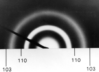
The present study was done on thin films of amorphous indium oxide . These were prepared in a vacuum chamber capable of achieving a base pressure of better than 310-7 mbar and equipped with electron-beam and Knudsen evaporation sources. Oxygen, cleaned by cold trap, could be bled into the chamber at controlled rates though a needle valve. Standard glass slides were used as substrates. These were chemically cleaned before being placed in the chamber. A setup for plasma cleaning of the substrates was used prior to deposition using pure oxygen. After plasma cleaning for a few minutes in an atmosphere of 210-1 mbar, the chamber was pumped down to better than 510-6 mbar. Films were prepared by e-beam evaporation of 99.999% pure pressed In2O3 pieces manufactured by Cerac as described in detail elsewhere 10 . A quartz crystal thickness monitor (calibrated against a Tolanski interferometer) was used to determine deposition rates and film thickness. The films used in this study were deposited at a rate of 1 Å/s to a nominal thickness of 200-250 Å. These conditions yield the relatively high carrier concentration ( samples with smaller than are not superconducting down to 1 K). The as-prepared films were studied by high resolution transmission electron microscopy and exhibited microstructure and diffraction patterns that are typical for amorphous structures (c.f., figure 1).
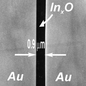
Samples for measuring large scale material properties and Hall-effect measurements were defined by placing an appropriate aluminum mask over the substrate during the deposition. To study the scale dependence, we compared the properties of batches of simultaneously prepared samples of common width and different lengths down to less than a micron. These were prepared by a liftoff technique; Strips of amorphous indium-oxide, 0.5 mm wide and few millimeters long were made using a mechanical mask. Thin fibers were then pulled from a drop of 7031-GE varnish and placed across the strip. The thickness of the fibers could be controlled in the range of 50m down to less than 0.2m by proper dilution of the varnish in a 1:1 solution of ethanol and toluene (varnish thinner), and by the speed at which the fibers were pulled. The slides were then returned to the vacuum chamber and a 300 Å layer of gold was deposited over the . Finally the slides were immersed in varnish thinner to dissolve the fibers and wash away the gold that was on them. This left a series of gaps in the gold layer which defined indium oxide samples all ”cut” from the same thin film, having a common width but different lengths. Longer samples could be made by using commercial copper wire instead of the varnish fibers. Electrical connections were made by soldering wires to small pieces of indium metal pressed onto the gold contacts. Before depositing the gold and after completing sample preparation the fibers/gaps were viewed through an optical microscope at x400 magnification to see the range of sample lengths obtained and their geometrical quality. Figure 2 shows a SEM micrograph of a 0.9m long sample. The borders were checked to bee smooth and equidistant over the entire width of the sample (500m) to within 10%.
III Results and discussion
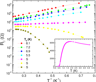
As prepared films of are usually insulating and exhibit negative temperature coefficient of resistivity from room temperatures down, and some form of variable range hopping may be observed at the 10-100 K range 10 . Samples that are near the SIT on the insulating side tend to show simple activation at liquid helium temperatures. Namely, is seen to follow with typical activation energy of order 3-15 K depending on disorder. This is true in 3D 11 as well as in the 2D regime 3 ; 4 ; 5 ; 6 ; 7 ; 8 and is still one of the important unsolved issues of transport near the SIT 12 . Figure 3 illustrates this behavior for a large-area film measured at several stages of annealing (disorder). Note that as the sheet-resistance at 4 K is reduced by annealing, so does the activation energy, and for 6 k the temperature dependence becomes rather weak. In fact, as shown in the inset, samples with this value of are superconducting below 0.3 K. A ‘critical’ may be thus identified at the value of 6 k for the SIT in this system. A similar value for has been reported by other researchers.
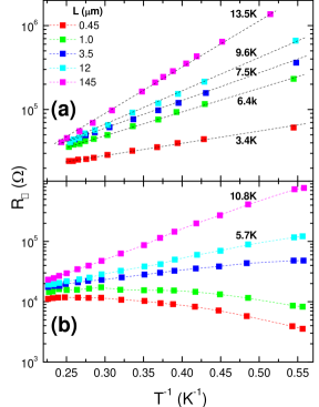
A somewhat different situation is encountered in the small-area samples. This is illustrated in figures 4a and 4b that show data for a single batch of samples at two stages of annealing and for samples with different length Note that has a marked dependence on (and/or the aspect ratio) and this leads to a significant variation of as the temperature is lowered (figure 4a). Upon further annealing (causing a decrease in the average disorder), this disparity makes for a sharper division of the data; The two longest samples in the batch are still activated with somewhat reduced relative to the previous stage. However, the two shortest samples of the same batch now show a clear tendency to become superconducting at low temperatures (figure 4b). This is a striking result as the samples are all made from the same batch and in fact show very similar resistances at higher temperature. Moreover, associating, as previously done, with the value of the sheet resistance that separates these two groups we now get a value that is at least twice larger than that of the large-area samples of the same material. It is emphasized that the length-controlling fibers were placed on the common strip in close proximity to one another and at no particular order (i.e., no hierarchy of along the strip), and therefore the dependence cannot be related to a ‘technological’ inhomogeneity.
These dependencies of the transport properties on sample scale and aspect ratio is suggestive of a percolation phenomena in an inhomogeneous media. As argued before 3 the inhomogeneity is a natural consequence of disorder, and inasmuch as superconductivity is concerned, the effect of disorder may be highly accentuated.
The argument is based essentially on the phenomenon of universal conductance fluctuation: Superconductivity usually vanishes when the average conductance of the 2D system is comparable with At this degree of disorder the conductance of the underlying diffusive metal fluctuates considerably on scales of order the phase-coherent length. In fact, the local conductivities are naturally distributed over a range, which means that at the transition to strong localization the distribution-width of the local conductances is of order unity. Therefore as the average critical disorder is attained, there are perforce some regions of the sample where the local disorder is smaller than critical and these regions may be locally superconducting. It is easy to see that from the point of view of conductivity the system may appear ‘granular’ with small superconducting regions embedded in an insulating matrix (and a complementary situation on the ‘weakly localized’ side of the transition). This may happen even in a structurally featureless amorphous structure as are the samples in the present case (as mentioned above, c.f., figure 1). Such a scenario is generic and should be pertinent for all materials where sub-critical disorder does not appreciably decrease . These then include all systems that obey the Anderson Theorem as well as metals that show ‘enhancement’ phenomena.

If one allows for just short-range disorder, these arguments cannot however account for the spatial scale over which the results in figures 4a and 4b are still size dependent. Gaussian disorder could conceivably lead to an inhomogeneous situation on scale of the order of evaluated at the measurements temperatures (or the percolation radius of the hopping problem on the insulating side of the transition). Neither of these lengths is larger than 1 m at liquid helium temperatures whereas significant size dependence is observed in our experiments up to that is at least one order of magnitude larger.
The relevant scale for the actual ‘granularity’ may of course be larger than the size of the individual superconducting island; several such islands may be Josephson-coupled to form a larger cluster. But this still leaves unanswered the scale dependence of the activation energy observed in figure 4a to extend over tens of microns. It would therefore seem necessary to consider the existence of long-range potential-fluctuations in these samples, which is not an uncommon phenomenon in amorphous materials 13 . In fact, long-range fluctuations in the disorder may be expected to be present when the disorder is large as must be the case here (strong disorder is actually required when a high carrier-concentration system is to be rendered Anderson localized). This is due to the cost of creating a potential gradient which would favor large potentials drops on the longer spatial scales. Naturally then, long range potential fluctuations should be a consideration especially when the sample is prepared or is later exposed to room (or higher) temperatures.
The presence of long-range potential-fluctuations in these films is also reflected in the current-voltage () characteristics of the studied samples. In their normal state all our samples showed deviations from Ohmic behavior above a characteristic voltage . These deviations were always such that which is presumably related to the fact that the temperature coefficient of the resistance is negative at helium temperatures. As a rule, the critical field at which non-linearity became important was noticeably larger at small This trend is illustrated in figure 5 for all the relevant samples used in our study. Despite the scatter in the data, it is clear that long samples are ”softer” than short ones as may be expected from long-range fluctuations; samples with larger are associated with with larger local fields hence they are more susceptible to non-linearity at any macroscopic field. Note that at which measurable deviations from Ohm’s law are observed is scale-dependent over the same range of where the data in figure 4a and 4b exhibit scale-dependence.
In summary, we have presented experimental evidence for the inhomogeneous nature of transport in an amorphous system near the SIT. The results seem to suggest the relevance of long-range potential-fluctuations which may result from thickness and/or composition variations to which characterization methods such as diffraction, STM, TEM, as well as other form of microscopy may not be as sensitive as charge transport. These issues clearly deserve further experimental and theoretical elucidation.
This research was supported by a grant administered by the US Israel Binational Science Foundation and by the Israeli Foundation for Sciences and Humanities.
References
- (1) Allen M. Goldman and Nina Markovic, Physics Today, November (1998) 39.
- (2) M. A. Paalanen, A. F. Hebard, and R. R. Ruel, Phys. Rev. Lett. 69, (1992) 1604.
- (3) D. Kowal and Z. Ovadyahu, Sol. St. Comm. 90 (1994) 783.
- (4) V. F. Gantmakher, M. V. Golubkov, J. G. S. Lok, and A. K. Geim, JETP 82, (1996) 951.
- (5) G. Sambandamurthy, L. W. Engel, A. Johansson, and D. Shahar, Phys. Rev. Lett. 92,(2004) 107005.
- (6) G. Sambandamurthy, L. W. Engel, A. Johansson, E. Peled, and D. Shahar, Phys. Rev. Lett., 94, (2005) 017003.
- (7) M. Steiner and A. Kapitulnik, Physica C 422, (2005) 16.
- (8) T. I. Baturina, J. Bentner, C. Strunk, M. R. Baklanov, and A. Satta, Physica B 359, (2005) 500; T. I. Baturina, C. Strunk, M. R. Baklanov, and A. Satta, cond-mat/0602557.
- (9) Yonatan Dubi, Yigal Meir, and Yshai Avishai, Phys. Rev. B 73, (2006) 054509.
- (10) Z. Ovadyahu, J. Phys. C 19, (1986) 5187.
- (11) D. Shahar and Z. Ovadyahu, Phys. Rev. B 46, (1992) 10917.
- (12) A possible mechanism has been recently offered by M. V. Feigel’man, L. B. Ioffe, V. E. Kravtsov, and E. A. Yuzbashyan, Phys. Rev. Lett. 98, (2007) 027001.
- (13) B. V. Fine, J. P. R. Bakker, and J. I. Dijkhuis, Phys. Rev. B 68, 125207 (2003); A. R. Long, Journal of Non-Crystalline Solids, 114, (1989) 348.