Screening model for nanowire surface-charge sensors in liquid
Abstract
The conductance change of nanowire field-effect transistors is considered a highly sensitive probe for surface charge. However, Debye screening of relevant physiological liquid environments challenge device performance due to competing screening from the ionic liquid and nanowire charge carriers. We discuss this effect within Thomas–Fermi and Debye–Hückel theory and derive analytical results for cylindrical wires which can be used to estimate the sensitivity of nanowire surface-charge sensors. We study the interplay between the nanowire radius, the Thomas–Fermi and Debye screening lengths, and the length of the functionalization molecules. The analytical results are compared to finite-element calculations on a realistic geometry.
Imagine a sensor so small and compact that it can fit almost everywhere and detect all kinds of chemical substances in real time. Such a sensor could in principle monitor and detect unwanted bacteria and viruses instantaneously in eg. your blood or drinking water. Sensors based on semiconductor nanowires have already been fabricated Cui:2001 and shown to work, for example as a pH sensor, where the concentration of hydrogen ions H+ in a surrounding liquid is detected Chen:2006 . Moreover, applications in label-free detection and biological sensing addressing e.g. DNA in low concentration is now being explored Zheng:2005b ; Wang:2005 ; Stern:2007 ; Carlen:2007 . In general, the conductance of a nanowire is in the literature considered a promising candidate for a highly sensitive probe of charged particles covering or situated near its surface. Detection limits have been studied theoretically with respect to binding-diffusion dynamics of the molecules at and near the surface Sheehan:2005 ; Nair:2006 . However, it is also crucial to address the fundamental problem of effective screening of these charges in physiologically relevant liquids which typically yield screening of charges on the nanometer length scale. Of course it is possible to decrease the salt concentration in the analyte solution, but this may not only complicate the process – it may also change the biological functions.
Effects of screening have been discussed qualitatively in the literature (see e.g. Refs. Cheng:2006, ; Stern:2007, ) touching on the influence from the competing screening mechanisms of the electron gas in the nanowire and the dissolved ions in the surrounding electrolyte. Very recently the effect has also been discussed in a computational study of a Silicon nanowire (SiNW) FET Heitzinger:2007 . In this Letter we develop a simple screening model which exemplifies how the desired screening of surface charge by the nanowire charge carriers may be jeopardized by the contending screening by the electrolyte. We derive analytical results for cylindrical wires which can be used to estimate the sensitivity of a nanowire surface-charge sensor surrounded by electrolyte. The analytical results are compared to finite-element calculations on a realistic geometry.
A surface charge density will perturb the initial charge-carrier density in the nanowire by , thus changing the initial conductance by . As an example, a positive surface charge will attract additional electrons from the nanowire contacts (equilibrium reservoirs). From simple conservation of charge we arrive at the following expression for the sensitivity
| (1) |
with being a dimensionless function, between zero and unity, quantifying the actual sensitivity in the presence of Debye screening in the electrolyte and a finite Thomas–Fermi screening in the nanowire. We show that scales with the electron density as in the dilute limit, thus leading to a prediction of a dependence, contrasting the intuitively expected dependence. However, high sensitivity is of course still associated with low densities.
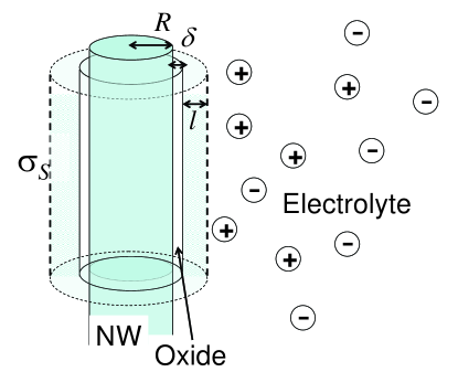
Above, is the perimeter of the of nanowire cross section (the fraction supporting the surface charge), is the cross-sectional area, and is the electron charge. For a cylindrical wire of radius we have , thus clearly illustrating the benefit of scaling the wires to the nano regime. Obviously, screening in the liquid will suppress the sensitivity below the bound given by Eq. (1) and a dependence (the limit ) can only be expected when the Thomas–Fermi screening in the nanowire is much stronger than the Debye screening in the electrolyte surrounding the nanowire so that changes in the density of the electron gas fully compensates the additional surface charge. In our screening model we consider the induced electrical potential due to a surface-charge density on the outside of an oxide-covered nanowire, see Fig. 1. For the nanowire we employ the Thomas–Fermi model (see e.g. Ref. Ashcroft:1976, ) while for the dilute electrolyte we consider a Debye–Hückel approximation (see e.g. Ref. Feynman:1964b, ). We these approximations we arrive at the following linear differential equation for the induced electrical potential ,
| (2a) | |||
| where is the Thomas–Fermi screening length in the nanowire domain and is the Debye screening length in the electrolyte domains and . The electrically insulating oxide-layer domain is free from charges and the potential is simply a solution to the Laplace equation. Obviously, the induced potential should vanish at infinity and denoting the solution in domain by and the corresponding dielectric function by we have the additional boundary conditions | |||
| (2b) | |||
where is a normal vector to the surface separating the neighboring domains and . Furthermore, is the corresponding surface-charge density. In the following we consider the case of a surface-charge density accumulated at the surface , i.e. and . For the dielectric function we have . The thickness of the domain is physically interpreted as the length of the functionalization molecules supporting the charge which for resides directly on the outside of the oxide-layer of the nanowire. In general the oxide layer will be charged unless the analyte solution equals the isoelectric point of the surface. Here we neglect this charge and assume that it may just shift the value of the initial carrier concentration in the wire.
In the following we consider the conductance of the nanowire of length and in particular we focus on the conductance change due to a finite surface-charge density . In terms of the electron mobility we have where is the electron density and is the electron charge. We determine the induced charge-density, , from the Poisson equation,
| (3) |
Formally, the conductance change can now be expressed in terms of the induced potential, i.e.
| (4) |
where is the conductance in the absence of surface charge.
Equation (4) is our general result for the relative conductance change expressed in terms of an integral over the surface-charge induced potential in the nanowire. Combined with Eqs. (2a) and (2b) it forms a starting point for analytical solutions of simple geometries or numerical solutions of more complicated geometries, e.g. by a finite-element method.
Before turning to more complicated geometries we first consider the case of a long cylindrical nanowire immersed in an infinite volume of electrolyte (see Fig. 1). The nanowire has a radius with an oxide-layer of thickness and due to the cylinder symmetry we may solve the problem analytically. For simplicity we focus on the, for experiments, highly relevant limit of an ultra-thin oxide layer. Furthermore, we consider so that the charge resides on the outside of the nanowire oxide layer. Solving the linear problem we then arrive at
| (5) |
which is easily verified to be a function ranging from zero in the limit to unity in the limit . We note that in the static limit, water is highly polarizable and while for silicon . Thus, for a fixed the ultimate sensitivity, Eq. (1) with , requires a very short Thomas–Fermi screening length, but at the same time one would like to benefit from the dependence originating from . We get in the range of – for at room temperature and ionic concentrations, , for typical physiological electrolytes. For example Heitzinger:2007 a realistic salt concentration (Na+Cl-) of 150 mM yields a screening length of thus calling for nanowires with densities supporting screening at the true nanometer scale. A simple estimate of also yields for a carrier concentration of cm-3. Taylor expanding Eq. (5) in the dilute carrier limit, , we get
| (6) |
so that we arrive at the scaling in Eq. (1).
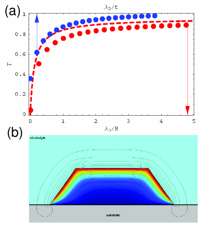
Figure 2a illustrates the dependence of the sensitivity on the Debye screening in the electrolyte. The lower trace is for a nanowire of circular cross section with . The solid lines shows Eq. (5) valid for a negligible oxide-layer thickness, i.e. while the data points are the result of finite-element simulations (Comsol MultiPhysics) taking into account a finite oxide layer of width and with . As seen, Eq. (5) accounts well for the numerical exact results. The upper trace shows finite element results for a nanowire with a trapezoidal cross section with aspect ratio , an etching defined angle of corresponding to the fabricated structure in Ref. Stern:2007, , see Fig. 2b. The oxide layer has a thickness and for the Thomas–Fermi screening we have which is somewhat stronger than for the circular case shown in the lower trace. Note how the two curves have the same overall shape and dependence on the Debye screening length, though the stronger Thomas–Fermi screening for the upper case makes approach unity for more moderate Debye screening lengths than in the lower case. Fig. 2b illustrates a typical distribution of the induced charge-carrier density in the nanowire and the superimposed contours show the equipotential lines. As expected the excess carrier density is induced near the surface of the wire supporting the surface-charge density .
Finally, let us discuss the prospects for sensing of point-like charges located at a distance further away from the conductor. Obviously, the additional Debye screening in the layer of thickness (see Fig. 1) will further reduce the induced carrier density in the nanowire and in a simple picture (neglecting curvature) we would qualitatively expect a reduction proportional to . In the following we let denote the average number of molecules absorbed on the wire of length and we imagine that the chain-like functionalization molecule supports a charged group, with charge , situated at a distance from the surface. Smearing out these charges results in an equivalent surface-charge density at . Solving the problem in Eqs. (2a) and (2b) for a finite we get with
| (7) |
Here, we have used the large-argument exponential asymptotes for the Bessel functions. The extra factor illustrates the additional, close-to-exponential, suppression by Debye screening when the charge is supported by a functionalization molecule of length . We note that in principle the entering the expression for could differ from the Debye screening length of the electrolyte e.g. due to the surface functionalization.
In conclusion, we have used Thomas–Fermi and Debye–Hückel theory to formulate a simple screening model for surface-charge sensing with conducting nanowires. The two screening mechanisms are playing in concert and our model illustrates the non-trivial interplay between the nanowire radius , the Thomas–Fermi Screening length , the Debye screening length , and the length of the functionalization molecules.
Acknowledgments. We thank Jesper Nygård, Brian Skov Sørensen, Per Hedegård, Troels Markussen, and Mogens H. Jakobsen for stimulating discussions.
References
- (1) Y. Cui, Q. Q. Wei, H. K. Park, and C. M. Lieber, Science 293, 1289 (2001).
- (2) Y. Chen, X. H. Wang, S. Erramilli, P. Mohanty, and A. Kalinowski, Appl. Phys. Lett. 89, 223512 (2006).
- (3) G. F. Zheng, F. Patolsky, Y. Cui, W. U. Wang, and C. M. Lieber, Nat. Biotechnol. 23, 1294 (2005).
- (4) W. U. Wang, C. Chen, K. H. Lin, Y. Fang, and C. M. Lieber, Proc. Natl. Acad. Sci. U. S. A. 102, 3208 (2005).
- (5) E. Stern, J. F. Klemic, D. A. Routenberg, P. N. Wyrembak, D. B. Turner-Evans, A. D. Hamilton, D. A. Lavan, T. M. Fahmy, and M. A. Reed, Nature 445, 519 (2007).
- (6) E. T. Carlen and A. van den Berg, Lab Chip 7, 19 (2007).
- (7) P. E. Sheehan and L. J. Whitman, Nano Lett. 5, 803 (2005).
- (8) P. R. Nair and M. A. Alam, Appl. Phys. Lett. 88, 233120 (2006).
- (9) M. M. C. Cheng, G. Cuda, Y. L. Bunimovich, M. Gaspari, J. R. Heath, H. D. Hill, C. A. Mirkin, A. J. Nijdam, R. Terracciano, T. Thundat, and M. Ferrari, Curr. Opin. Chem. Biol. 10, 11 (2006).
- (10) C. Heitzinger and G. Klimeck, Journal of Computational Electronics 6, 387 (2007).
- (11) N. W. Ashcroft and N. D. Mermin, Solid State Physics (Saunders College Publishing, San Diego, 1976).
- (12) R. Feynman, R. B. Leighton, and M. L. Sands, The Feynman lectures on physics (Addison-Wesley Publishing Company, Reading, Massachusetts, 1964), Vol. 2.