Hybrid single-electron transistor as a source of quantized electric current
††preprint:The basis of synchronous manipulation of individual electrons in solid-state devices was laid by the rise of single-electronics about two decades ago averin91 ; SET92 ; devoret92 . Ultra-small structures in a low temperature environment form an ideal domain of addressing electrons one by one. A long-standing challenge in this field has been the realization of a source of electric current that is accurately related to the operation frequency averin91 . There is an urgent call for a quantum standard of electric current and for the so-called metrological triangle, where voltage from Josephson effect and resistance from quantum Hall effect are tested against current via Ohm’s law for a consistency check of the fundamental constants of Nature, and piquemal04 . Several attempts to create a metrological current source that would comply with the demanding criteria of extreme accuracy, high yield, and implementation with not too many control parameters have been reported. However, no satisfactory solution exists as yet despite many ingenious achievements that have been witnessed over the years geerligs90 ; pothier92 ; keller96 ; shilton96 ; fujiwara04 ; delsing05 ; vartiainen06 . Here we propose and prove the unexpected concept of a hybrid metal-superconductor turnstile in the form of a one-island single-electron transistor with one gate, which demonstrates robust current plateaus at multiple levels of within the uncertainty of our current measurement. Our theoretical estimates show that the errors of the present system can be efficiently suppressed by further optimizations of design and proper choice of the device parameters and therefore we expect it to eventually meet the stringent specifications of quantum metrology.
Synchronized sources, where current is related to frequency by and is the integer number of electrons injected in one period, are the prime candidates for the devices to define ampere in quantum metrology. The accuracy of these devices is based on the discreteness of the electron charge and the high accuracy of frequency determined from atomic clocks. Modern methods are replacing classical definitions of electrical quantities; voltage can be derived based on the AC Josephson effect of superconductivity shapiro63 and resistance by quantum Hall effect klitzing80 ; paalanen82 , but one ampere still needs to be determined via the mutual force exerted by leads carrying the current. Early proposals of current pumps for quantum metrology were based on arrays of mesoscopic metallic tunnel junctions geerligs90 ; pothier92 , in which small currents could eventually be pumped at very low error rates keller96 . However, these multijunction devices are hard to control and relatively slow zimmerman03 . Thus, the quest for feasible implementation with a possibility of parallel architecture for higher yield have lead to alternative solutions such as surface-acoustic wave driven one-dimensional channels shilton96 , superconducting devices niskanen03 ; zorin04 ; governale05 ; kopnin06 ; mooij06 ; vartiainen06 ; cholascinski07 , and semiconducting quantum dots ritchie07 . These do produce large currents in the nano-ampere range but their potential accuracy is still limited.
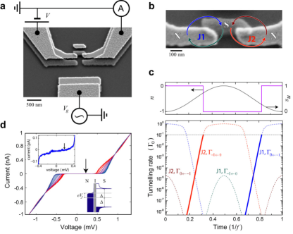
Somewhat surprisingly, a simple hybrid single-electron transistor, with normal metal (N) leads and a small superconducting (S) island, see Fig. 1, has been overlooked in this context. As it has turned out in the present work, an SNS-transistor, or alternatively an NSN-transistor, presents ideally a robust turnstile for electrons showing accurately positioned current plateaus. We emphasize here that a one island turnstile does not work even in principle without the hybrid design. An important feature in the present system is that hybrid tunnel junctions forbid tunnelling in an energy range determined by the gap in the density of states of the superconductor, see Fig. 1d inset; current through a junction vanishes as long as .
Figure 1a shows the simple electric configuration to operate a hybrid turnstile. A DC bias voltage is applied between the source and drain of the transistor and a voltage with DC and AC components at the gate. To understand the operation of the turnstile on a more quantitative level, let us follow a basic operation cycle shown in Fig. 1c. In general, a sinusoidal AC gate voltage is superposed on the DC offset such that the total instantaneous voltage on the gate, normalized into charge in units of , reads at frequency . Here is the capacitance of the gate electrode to the transistor island. In Fig. 1c we have chosen the gate offset and amplitude to be , and the bias voltage across the transistor is set at to suppress tunnelling errors, as will be discussed below. The key point in the operation of the hybrid turnstile is that the charge state locks to a fixed value in any part of the operational cycle except at the moment when a desired tunnelling event occurs. This is the key feature of the device, originating from the interplay of the superconducting gap in the energy spectrum and Coulomb blockade of single-electron tunnelling. It renders this structure to work as an accurate turnstile where errors can be suppressed efficiently by decreasing temperature and by choosing the bias point properly within the superconducting gap. This locking mechanism is illustrated and explained in Fig. 1c for one operational cycle. On the contrary, in the biased NNN transistor with Coulomb blockade alone, non-synchronized almost frequency independent DC current through the device is observed SET92 . Likewise, a corresponding fully superconducting SSS device is not favourable either, because inevitable supercurrent of Cooper pairs induces significant leakage errors zorin03 .
Several hybrid turnstiles with aluminium as the superconductor, copper as the normal metal, and aluminium oxide as the tunnel barrier in between were fabricated by standard electron beam lithography. Both the aluminium and the copper films were 50 nm thick. Figure 1a shows the NSN sample whose data we present here. The charging energy of the aluminium island, , is K, where is the total capacitance. The sum of the tunnel resistances of the two junctions is 700 k, i.e., 350 k per junction on the average. The current-voltage () characteristics of the transistor are shown in Fig. 1d at various values of the DC gate voltage and with no AC gate voltage applied. The superconducting gap suppresses the current strongly in the bias region mV. Outside this region the typical gate modulation pattern shows up SET92 . The charging energy of the device was determined based on the envelopes of these curves.

The turnstile experiments were carried out by voltage biasing the transistor at , highlighted by an arrow in Fig. 1d. Figure 2 shows the current through the NSN turnstile under varying parameters , and at a fixed frequency MHz. Figure 2c shows cross-sections of the 3D plot in Fig. 2a along different constant values of against the gate amplitude . The corresponding prediction based on sequential tunnelling theory averin91 is shown by the dashed lines in the same plot. The experimental data follow the theoretical prediction very closely. Moreover, the wide flat plateaus at seem indeed promising for metrological purposes. The magnitude of the pumped current is robust against fluctuations in relevant parameters. It is not sensitive to exact dimensions or symmetry of the device, operational temperature, gate offset or its amplitude, or the exact form of the driving signal in general. Some of these dependencies are demonstrated in Fig. 2d based on our present measurements.
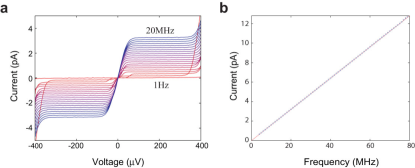
Figure 3 illustrates the frequency dependence of the NSN turnstile. In Fig. 3a we show the curves measured for at various frequencies. The frequency dependence of the current corresponding to the first plateau in measurements of the type that were shown in Fig. 2b is plotted in Fig. 3b against in the frequency regime up to 80 MHz. The predicted relation is followed closely within smaller than 1% deviations in absolute current throughout this range. We stress here that in the present measurement, using just a room temperature current amplifier, we cannot test the agreement between the prediction and the absolute value of the measured current to any higher degree than this.
Next we discuss the choice of the operating conditions of a hybrid turnstile and the potential accuracy of this device. Within the classical model of sequential single-electron tunnelling, the bias voltage across the turnstile is a trade-off: small bias leads to tunnelling events in the backward direction and large to errors due to replacement of the tunnelled charge by another one tunnelling in the forward direction through the other junction. Unwanted events of the first type occur at the relative rate of , where is the temperature of the normal metal electrodes. Errors of the second type occur at the relative rate of . The prefactor of this expression is of the order of unity in relevant cases of interest. Minimizing these errors thus yields , which is chosen as the operation point in the experiments. At this bias point the two errors are of order . For eV (aluminium) and mK that is a standard range of operation temperature, we obtain an error rate of , which is sufficiently small as compared to the requested accuracy of the metrological source piquemal04 .
The analysis above neglects several types of errors. High operation frequency is one source of error: it leads to missed tunnelling events and to enhanced tunnelling in the wrong direction. These errors are suppressed approximately as . For typical parameters, for aluminium and k, we then request GHz for accurate operation. Such a small value of seems acceptable because of sufficiently strong suppression of co-tunnelling effects in this system as will be discussed below. With exponential suppression of errors in , the metrological accuracy limits then the frequency to MHz for turnstiles with aluminium as the superconductor. A possible way to increase the speed of the device is to use niobium as the superconductor, with almost an order of magnitude larger gap. With ultrasmall junctions, to keep , which is another criterion to satisfy in order not to miss any tunnelling events at the chosen bias point, one would be able to increase the frequency, and the synchronized current, by the same order of magnitude. This is an attractive yet unexplored possibility. Additional improvement, about factor of 3 increase in current, could possibly be achieved by shaping the ac gate voltage to have rectangular waveform.
Another source of potential errors is the co-tunnelling averin90 , i.e., higher order quantum tunnelling processes, which are limiting the use of short arrays in normal-metal-based devices martinis92 . In a hybrid turnstile, the lowest order quasiparticle co-tunnelling errors are, however, suppressed ideally to zero within the superconducting gap as has been shown for a fully superconducting case in the past averin97 . Another process of the same order which is not suppressed by the superconducting gap is the tunnelling of Cooper pairs, also called Andreev reflection. In junctions without pinholes in the barriers, the rate of this tunnelling should be quite small, , where the effective number of the transport modes in the junction of area can be estimated as m2 joyez98 . If the charging energy is large, , it suppresses direct tunnelling of Cooper pairs. Analysis shows that the lowest-order process that limits the accuracy of the hybrid turnstiles with ideal superconducting electrodes is then the co-tunnelling of one electron and one Cooper pair, the rate of which can be estimated roughly as . These processes are suppressed to the level mandated by the metrological accuracy, but one may need to increase the junction resistance to k. Further compromise in the operation frequency would not be necessary even in this case if one benefits from the improvements in the turnstile operation discussed above.
Sub-gap leakage, due, for instance, to non-zero density of quasiparticle states within the gap, introduces a material- and fabrication-specific source of errors into our system. This effect is demonstrated by the non-vanishing slope of the curve in the top inset of Fig. 1d and by an equal slope in the bias dependence of the bottom panel in Fig. 2d showing the current on the first plateau. Our estimates show that as far as co-tunnelling is concerned, such errors are small already in the present devices. For sequential tunnelling sub-gap leakage causes a substantial additional contribution to current, of order in the present device. With high quality tunnel junctions, possibly by an improved fabrication process, its influence can be suppressed further. Furthermore, the separation of the current plateaus, with one bias polarity only, is ideally not sensitive to this effect, unlike the absolute value of current on a single plateau. Yet we find the sub-gap leakage as the main issue to be solved in order to realize a metrologically compatible turnstile. We would also like to point out that a series connection of a few SN junctions would present an improved version of a multijunction electron pump pothier92 ; keller96 in terms of leakage and co-tunnelling errors, since this device can be operated without external bias voltage.
There is a difference between the performance of the SNS and NSN structures, which was not emphasized in the discussion above. The charge transport in these systems is associated with non-trivial heat flux: based on the same strategy as discussed here a single-electron refrigerator can be realized pekola07 ; saira07 . In this device superconductor is always heated, but under proper bias conditions heat flows out from the normal metal. Therefore, in a single island realization, an SNS configuration is more favourable, at least theoretically, as compared to the NSN turnstile. It turns out that with quite realistic parameters it is possible to refrigerate the small, thermally well isolated N island of an SNS turnstile substantially, and hence the error rates can be further suppressed. The source and drain leads can be thermalized close to the bath temperature by proper choice of geometry and materials. Cooling or overheating effects were, however, not identified definitely in the present experiment, where small errors () could not be assessed.
One of the key advantages of the single-island turnstile, as compared to multi-island pumps is that the influence of the background charges backgroundcharges can be compensated by adjusting just a single DC gate voltage, e.g., to maximize the width or minimize the slope of the current plateaus. Therefore the level of the current can be increased by a relatively straightforward parallelization of several turnstiles. If an upgrade of current by, for example, an order of magnitude is necessary, DC-gate setting of each of the ten turnstiles can be adjusted individually whereafter the currents of them can be combined. The whole device can then be operated with common-to-all DC bias and AC gate drive.
References
- (1) Averin, D. V. & Likharev, K. K. Single electronics: a correlated transfer of single electrons and Cooper pairs in systems of small tunnel junctions, in Mesoscopic phenomena in solids, edited by B. L. Altshuler, P. A. Lee and R. A. Webb, pp. 173-271 (North-Holland, Amsterdam, 1991).
- (2) Single charge tunneling - Coulomb blockade phenomena in nanostructures, edited by H. Grabert and M. H. Devoret (Plenum, New York, 1992).
- (3) Devoret, M. H., Esteve, D. & Urbina, C. Single-electron transfer in metallic nanostructures, Nature 360, 547-553 (1992).
- (4) Piquemal, F. et al. Fundamental electrical standards and the quantum metrological triangle, C.R. Physique 5, 857-879 (2004).
- (5) Geerligs, L. J. et al. Frequency-locked turnstile device for single electrons, Phys. Rev. Lett. 64, 2691-2694 (1990).
- (6) Pothier, H., Lafarge, P., Urbina, C., Esteve, D. & Devoret, M. H. Single-electron pump based on charging effects, Europhys. Lett. 17, 249-254 (1992).
- (7) Keller, M. W., Martinis, J. M., Zimmerman, N. M. & Steinbach, A. H. Accuracy of electron counting using a 7-junction electron pump, Appl. Phys. Lett. 69, 1804-1806 (1996).
- (8) Shilton, J. M. et al. High-frequency single-electron transport in a quasi-one-dimensional GaAs channel induced by surface acoustic waves, J. Phys.: Condens. Matter 8, L531-L539 (1996).
- (9) Fujiwara, A., Zimmerman, N. M., Ono, Y. & Takahashi, Y. Current quantization due to single-electron transfer in Si-wire charge-coupled devices, Appl. Phys. Lett. 84, 1323-1325 (2004).
- (10) Bylander, J., Duty, T. & Delsing, P. Current measurement by real-time counting of single electrons, Nature 434, 361-364 (2005).
- (11) Vartiainen, J. J., Möttönen, M., Pekola, J. P. & Kemppinen, A. Nanoampere pumping of Cooper pairs, Appl. Phys. Lett. 90, 082102 (2007).
- (12) Shapiro, S. Josephson currents in superconducting tunneling: the effect of microwaves and other observations, Phys. Rev. Lett. 11, 80-82 (1963).
- (13) v. Klitzing, K., Dorda, G. & Pepper, M. New method for high-accuracy determination of the fine-structure constant based on quantized Hall resistance, Phys. Rev. Lett. 45, 494-497 (1980).
- (14) Paalanen, M. A., Tsui, D. C. & Gossard, A. C. Quantized Hall effect at low temperatures, Phys. Rev. B 25, 5566-5569 (1982).
- (15) Zimmerman, N. M. & Keller, M. W. Electrical metrology with single electrons, Meas. Sci. Technol. 14, 1237-1242 (2003).
- (16) Niskanen, A. O., Pekola, J. P. & Seppä, H. Fast and accurate single-island charge pump: Implementation of a Cooper pair pump, Phys. Rev. Lett. 91, 177003 (2003).
- (17) Lotkhov, S. V., Bogoslovsky, S. A., Zorin, A. B. & Niemeyer, J. Radio-frequency-induced transport of Cooper pairs in superconducting single electron transistors in a dissipative environment, J. Appl. Phys. 95, 6325-6331 (2004).
- (18) Governale, M., Taddei, F., Fazio, R. & Hekking, F. W. Adiabatic pumping in a superconductor-normal-superconductor weak link, Phys. Rev. Lett. 95, 256801 (2005).
- (19) Kopnin, N. B., Mel’nikov, A. S. & Vinokur, V. M. Resonance energy and charge pumping through quantum SINIS contacts, Phys. Rev. Lett. 96, 146802 (2006).
- (20) Mooij, J. E. & Nazarov, Yu. V. Superconducting nanowires as quantum phase-slip junctions, Nature Physics 2, 169 - 172 (2006).
- (21) Cholascinski, M. & Chhajlany, R. W. Stabilized parametric Cooper-pair pumping in a linear array of coupled Josephson junctions, Phys. Rev. Lett. 98, 127001 (2007).
- (22) Blumenthal, M. D. et al. Gigahertz quantized charge pumping, Nature Physics 3, 343-347 (2007).
- (23) Lotkhov, S. V., Bogoslovsky, S. A., Zorin, A. B. & Niemeyer, J. Cooper pair cotunneling in single charge transistors with dissipative electromagnetic environment, Phys. Rev. Lett. 91, 197002 (2003).
- (24) Averin, D. V. & Nazarov, Yu. V. Virtual electron diffusion during quantum tunneling of the electric charge, Phys. Rev. Lett. 65, 2446-2449 (1990).
- (25) Jensen, H. D. & Martinis, J. M. Accuracy of the electron pump, Phys. Rev. B 46, 13407-13427 (1992).
- (26) Averin, D. V, Korotkov, A. N., Manninen, A. J. & Pekola, J. P. Resonant tunneling through a macroscopic charge state in a superconducting single slectron transistor, Phys. Rev. Lett. 78, 4821-4824 (1997).
- (27) Joyez, P., Esteve, D. & Devoret, M. H. How is the Coulomb blockade suppressed in high-conductance tunnel junctions?, Phys. Rev. Lett. 80, 1956-1959 (1998).
- (28) Pekola, J. P., Giazotto, F. & Saira, O.-P. Radio-frequency single-electron refrigerator, Phys. Rev. Lett. 98, 037201 (2007).
- (29) Saira, O.-P. et al. Heat transistor: demonstration of gate-controlled electron refrigeration, Phys. Rev. Lett., in press (2007).
- (30) Krupenin, V. A. et al. Noise in Al single electron transistors of stacked design, J. Appl. Phys. 84, 3212-3215 (1998).
Acknowledgements We thank Mikko Paalanen and Antti Manninen
for fruitful discussions, and Antti Kemppinen for assistance in the
measurements. The work was financially supported by Technology
Industries of Finland Centennial Foundation and by Academy of
Finland. M. M. acknowledges
the Finnish Cultural Foundation for financial support.