Incompatibility of modulated checkerboard patterns with the neutron scattering resonance peak in cuprate superconductors
Abstract
Checkerboard patterns have been proposed to explain the real space structure observed in STM experiments on BSCCO and Na-CCOC. However, simple checkerboard patterns have low energy incommsensurate (IC) spin peaks rotated 45 degrees from the direction of the charge IC peaks, contrary to what is seen in neutron scattering. Here, we study modulated checkerboard patterns which can resolve the low frequency inconsistency. Using spin wave theory, we explore the spin response of these superstructures and find that the high energy response is inconsistent with neutron scattering results. In particular, the modulated checkerboard structures are incapable of supporting the experimentally well-established resonance peak at ().
pacs:
74.25.Ha, 74.72.-h, 75.30.Ds, 76.50.+gI Introduction
Spin and charge ordering have been topics of great interest in strongly correlated electronic systems. A key aspect of many strongly correlated models is that different terms in the Hamiltonian compete, which introduces a type of electronic frustration since solutions cannot be found which simultaneously minimize all terms in the Hamiltonian. These competing interactions can lead to spontaneous nanoscale electronic structure. Indeed, several locally inhomogenous electronic phases have been proposed, involving charge order, spin order, and orbital order among others, in strongly correlated materials such as cuprate superconductors, nickelates, manganites, and related perovskites. Charge order is amenable to detection through probes that directly measure charge degrees of freedom, such as scanning tunneling microscopy (STM),hoffman ; checknccoc while the presence of spin order can be directly detected through neutron scattering.tranquadareview ; ybco ; john ; boothroyd03a ; boothroyd05 ; boothroyd06 Unfortunately, the charge patterns which most naturally explain the STM data have often been incompatible with the spin patterns which most simply explain the neutron scattering data. Part of the challenge has been that materials which are most amenable to STM studies (i.e. strongly layered materials) are least amenable to neutron scattering (which requires large crystals), and vice versa. Further complicating a clear and consistent interpretation of the data set as a whole is that while neutron scattering is a bulk probe, STM is confined to the surface.
Recent experimental advances have made possible the detection of high energy neutron scattering spectra hayden04 ; tranquada04a ; buyers04 . This has led to the discovery that the magnetic excitations in several cuprates, i.e., La2-xBaxCuO4 (LBCO), La2-xSrxCuO4 (LSCO), and YBa2Cu3O6+δ (YBCO), exhibit universal behavior tranquada04a ; hayden04 ; tranquada-schrieffer ; tranquada-universal . One prominent feature is that at intermediate energies, there is a resonance peakkeimer95 at formed by the merging of the low energy incommensurate response with a high energy response whose incommensurate structure is rotated from that of the low energy excitations. The resonance peak is observed in the pseudogap regime (i.e. the low temperature normal state of the underdoped cuprates), but sharpens as temperature is lowered into the superconducting state. The relation between the resonance peak and the emergence of superconductivity is still under research.tranquada06 The magnetic excitations in these materials have been explained using stripes, a unidirectional modulation of spin and charge. vojta-ulbricht ; uhrig04a ; tranquada04a ; seibold04 ; yao06a ; yaocarlson06b . In these models, the resonance peak is a saddlepoint in the dispersion.
STM can directly detect charge order at the surface. Checkerboard patterns (a two-dimensional modulation of charge) have been proposed to explain the real space structure observed in STM experiments on Bi2Sr2CaCu2O8+δ hoffman (BSCCO) and Ca2-xNaxCuO2Cl2 checknccoc (Na-CCOC). The charge modulations were characterized by checkerboad patterns with spacing approximately , where is the lattice spacing. While this spacing is in agreement with the incommensurability observed in neutron scattering, the presence of a true two-dimensional modulation such as a checkerboard has not been confirmed by neutron scattering or other bulk probes.
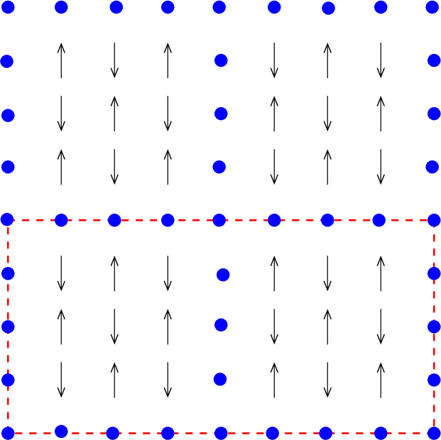
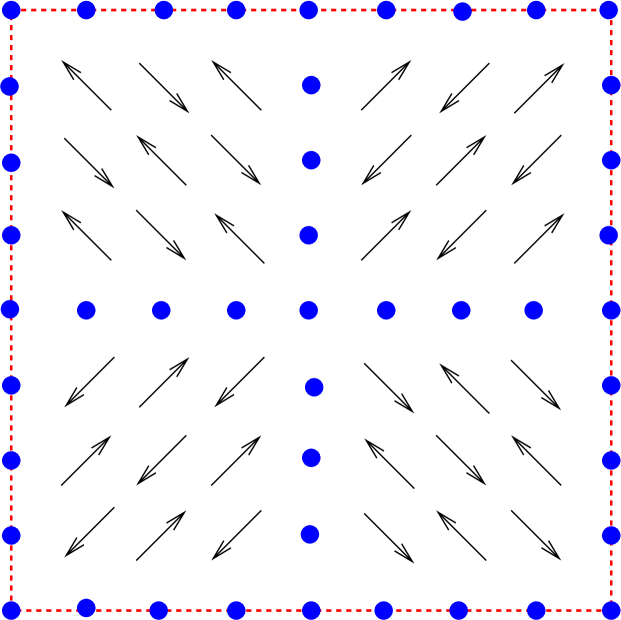
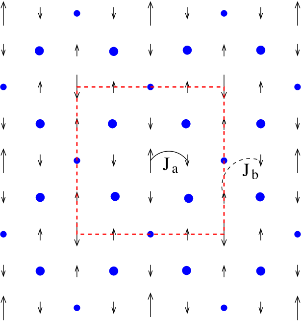
Within microscopic models, either stripes or checkerboards can be stabilized by tuning parameters, such as the next-nearest neighbor hopping .seibold06 The most natural checkerboard patterns to arise out of microscopic models are “simple” checkerboards, such as the one shown in Fig. 1(a). Such simple checkerboards are in fact ruled out experimentally, because the low energy charge peaks are rotated from the low energy spin peaks, contrary to what is observed in neutron scattering.tranquada-schrieffer ; vojta-sachdev ; andersen03 ; yaocarlson06b Later, modulated checkerboards were proposed, fine04 ; boothroyd06 as shown in Fig. 1(c) and 1(d). Recent experimental work has ruled out the modulated checkerboards in La1.48Nd0.4Sr0.12CuO4, based on the relative intensities of the incommensurate (IC) spin peaks in different magnetic Brillouin zones.boothroyd06 The authors of Ref. boothroyd06, also proposed a new noncollinear checkerboard pattern as shown in Fig. 1(b), which is consistent with all of the low energy data. We show here that for modulated checkerboards there is no possibility of a resonance peak at (), which rules out these structures in all materials where a resonance peak has been observed. We further argue that the newly proposed noncollinear checkerboard also lacks a resonance peak.
II Model and Method
In this paper, we study the magnetic excitations of various checkerboard patterns. Simple checkerboards of the type shown in Fig. 1(a) have been studied previously by us and othersyaocarlson06b ; vojta-sachdev ; andersen03 . These types of patterns, in which the sign of the Néel vector changes across each charge line (whether vertical or horizontal), are always found to have incommensurate (IC) spin peaks which are rotated from the IC charge peaks, contrary to what is observed in experiment from STM (which can measure the charge peaks), and neutron scattering (which can measure the spin peaks, and sometimes also the charge peaks as well). Modulated checkerboards, like those shown in Figs. 1(c) and 1(d) offer a consistent description of the low energy data, as does the noncollinear checkerboard shown in Fig. 1(b). Here, we extend our previous work on the magnetic excitations of stripes and simple checkerboards to the modulated and noncollinear checkerboard patterns.
We study the spin excitations within the Heisenberg model,
| (1) |
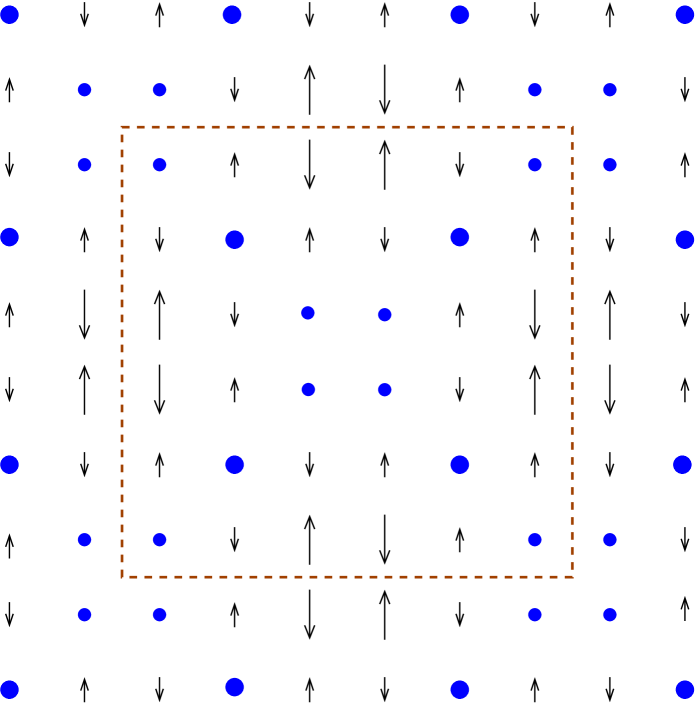
where the indices and run over all spin sites, and represents the spin coupling. We have assumed that the charge degrees of freedom can be integrated out to produce the effective spin couplings of the model. The main effect of the charge degrees of freedom is to form antiphase domain walls across which the Néel vector of the spins changes sign. As shown in Fig. 1(c), nearest neighbor couplings are (antiferromagnetic), and next-nearest neigbor couplings across a domain wall are (also antiferromagnetic). We make the physically reasonable assumption that is small compared to . The dotted lines in Fig. 1 show the unit cells. Note that in Figs. 1(c) and 1(d), the charge domain walls run diagonally. In Fig. 1(c), the diagonal spacing between domain walls is in units of the diagonal spacing . This configuration has spins in the unit cell. In Fig. 1(d) the diagonal spacing between domain walls is in the same units, and there are spins in the unit cell. For Figs. 1(c) and 1(d), the spin ground states shown are unfrustrated, there is long range magnetic order, and the elementary excitations can be captured by the spin wave treatment below. Note that the noncollinear checkerboard is not a ground state of this spin model. We will return to the magnetic excitations of this state later.
In order to study the magnetic excitations, we use the spin wave method to calculate the magnon excitation spectrum and the zero-temperature dynamic structute factor
| (2) |
where is the magnon vacuum state and denotes the final state of the spin system with excitation energy . is proportional to the expected neutron scattering intensity. We show two different sizes of spins in Figs. 1(c) and 1(d). We take the component of the larger spins to be twice that of the smaller spins, in order to take into account that the spin modulation is not a square wave. However, our major conclusions are independent of the details of this spin ratio.
III Results
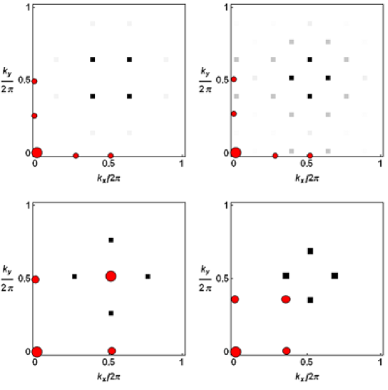
We first discuss the zero-frequency response, shown in Fig. 2. The greyscale image shows the expected diffraction peaks and relative intensities from the spin texture for each panel from Fig. 1. The diffraction peaks from the corresponding charge modulation are denoted schematically by the red circles, for fiduciary points around (0,0). For simple checkerboards, spin diffraction peaks are rotated 45 degrees from the direction of charge diffraction peaks, unlike what is seen in experiment. For the noncollinear checkerboard of Fig. 1(b) and the modulated checkerboards of Figs. 1(c) and 1(d), the relative orientation of the main spin and charge IC peaks are consistent with experiment. The noncollinear checkerboard gives more satellite peaks than the modulated checkerboards, even when the spacing of the noncollinear checkerboard is comparable to that of the modulated checkerboards, which may help distinguish these patterns. However, the higher harmonic spin peaks get weaker with increasing . For the experimentally relevant case of , the main IC peaks are nine times stronger than the next nonzero harmonic peaks, which may make them difficult to detect. Note that for modulated checkerboards of even spacing ( even), there is a charge diffraction peak located at (), contrary to what is observed in experiment. The strength of this peak decreases as the charge profile is made smoother.
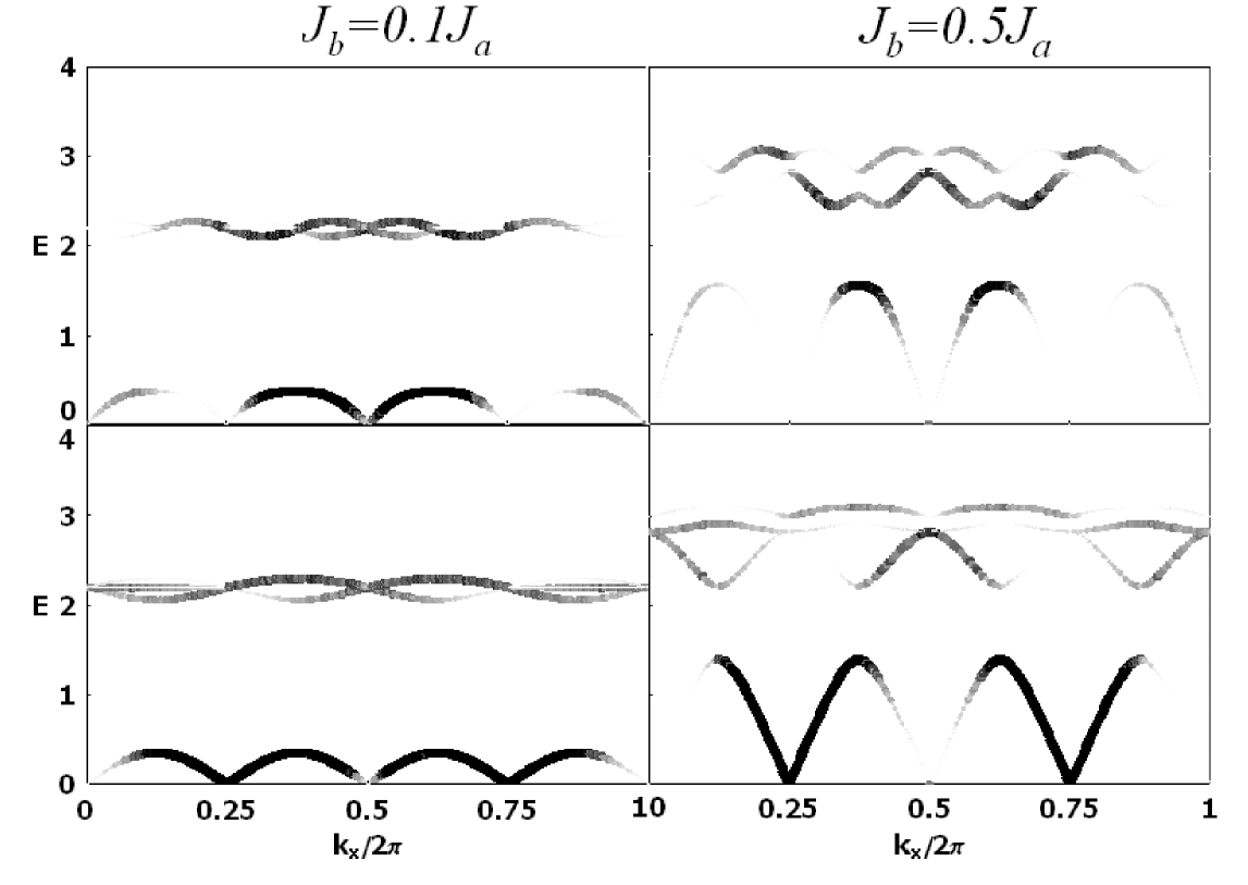
Spin wave dispersions with intensities for the modulated checkerboard case are shown in Fig. 3 at and along the and directions. Note that although zero-frequency weight is forbidden at because of the presence of antiphase domain walls in the Néel vector, nevertheless, the point is a reciprocal lattice vector, and so the spin-wave dispersion must approach at this wavevector. There are several defining characteristics of the resonance peak, but the most well-established is that the mode occurs at finite frequency. The reciprocal lattice structure of the modulated checkerboard patterns therefore forbids the appearance of a resonance peak in the acoustic band.
For comparison, the simple checkerboard patterns we studied in Ref. yaocarlson06b, are also incapable of supporting a resonance peak in the acoustic band, but for a different reason. In these cases, is not a reciprocal lattice vector, and so the acoustic mode at has finite frequency. However, in the case of simple checkerboards, the acoustic band reaches a local maximum at , rather than the saddlepoint found in stripe phases. The saddlepoint structure has been shown to capture the phenomenology of the resonance peak,yaocarlson06b ; vojta-sachdev ; uhrigsaddlepoint including the finite-frequency peak in the integrated spin structure factor , as well as the presence of incommensurate scattering which smoothly connects to the resonance peak both below and above it in frequency. By contrast, while the simple checkerboards have a peak in at finite frequency, there is no weight immediately above the point in frequency. This is one of a few reasons why simple checkerboard patterns have been ruled out.
For the modulated checkerboards studied here, one may consider the possibility of the resonance peak appearing in one of the optical bands. There is a gap between the acoustic band and optical bands, similar to the simple checkerboard configurations. yaocarlson06b The gap is sizable when is small. The acoustic band begins to touch the optical bands at . For the physically reasonable assumption that is smaller than , any weight appearing in an optical band at is too far removed from the incommensurate scattering at low frequency to be a candidate for the resonance peak. Furthermore, the lack of a saddlepoint structure in the optical bands further rules out a resonance peak-like structure (see Fig. 3, where instead of a saddlepoint, two bands cross at ).
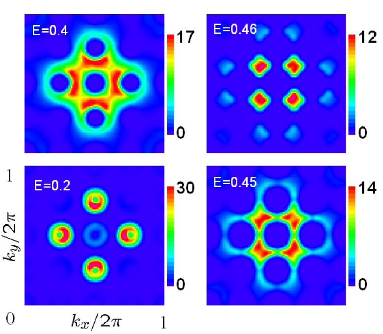
Constant energy cut plots are experimentally measurable and useful for analyzing the microscopic structures. Fig. 4 shows representative constant energy cut plots for the structure of Fig. 1(c), at coupling ratio . For the modulated checkerboards, it is clear that the direction of the low energy IC spin peaks are consistent with that observed experimentally for the low energy IC charge peaks, whereas this was not the case for simple checkerboards. We find that although a spin-wave cone must be present at low energy, the intensity of the spin structure factor is not uniform on the cone, as shown in the panel. As in our previous studies of arrays of antiphase domain walls (whether in stripe or simple checkerboard patterns),yaocarlson06b for small coupling ratio , the intensity is strongest on the inner branch of the spin wave cone, i.e. the side closest to the point. We take this to be a generic feature of spins which are weakly coupled across arrays of antiphase domain walls.
Note also the presence of a faint spin wave cone emanating from the point. This spin wave cone is required by symmetry, since the point is a reciprocal lattice vector of the modulated checkerboard structures. However, due to the antiphase domain walls, weight is forbidden at zero frequency at and this makes the central cone quite faint at finite frequency compared to those emanating from the main IC points. At intermediate energies (), the spin wave cones touch each other. At higher energies, just below the top of the acoustic band, incommensurate peaks are once more observed, now rotated to the diagonal direction, as shown in the panel. Note the complete absence of weight at the point, precluding a resonance peak from this type of modulated checkerboard.
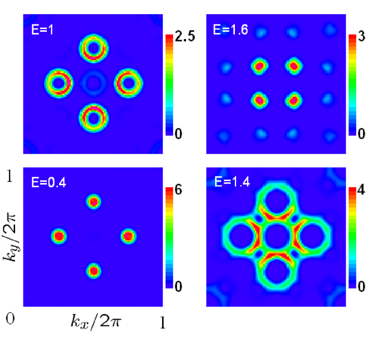
For comparison, in Fig. 5 we show similar constant energy cuts, with a stronger coupling ratio . These have a steeper dispersion (as is evident from Fig. 3), and the spin wave cones appear simply as incommensurate peaks in the lowest energy panel, . As energy increases, the spin wave cones become visible as shown for . As with the weaker coupling case, the intensities are not uniform on the spin wave cone, and the intensities peak on the side facing . Note that at this energy, the faint spin-wave cone emanating from becomes visible. At higher energies (), the spin wave cones merge. At yet higher energies (), the top of the acoustic band produces incommensurate peak structure at finite frequency, with peaks rotated from the low energy IC peaks. As with the weaker coupling ratio, the acoustic band is forbidden by symmetry to support any weight at the point, ruling out these structures as being able to support a resonance peak.
We now briefly comment on the noncollinear checkerboard proposed in Ref. boothroyd06, and reproduced schematically in our Fig. 1(b). Like the modulated checkerboard patterns, this pattern has IC spin peaks which are in the same direction as the main IC charge peaks, consistent with low energy experimental data. While modulated checkerboards have been challenged based on the experimental results of Ref. boothroyd06, , the authors were unable to definitively rule out the noncollinear checkerboard (“two- structure”). We are not able to calculate the expected magnetic excitation spectrum within the framework of the current model, since this pattern is not a valid ground state of the Hamiltonian we consider here (see Eqn. 1.) This does not preclude it being the ground state of some other model. What we can say about this structure is that to the extent that it supports Goldstone modes, it will have the same limitations of the modulated checkerboard patterns discussed here. This is because the point is a reciprocal lattice vector of the noncollinear checkerboard, and so it is constrained by symmetry to have a spin wave cone emanating from the point. This point is also forbidden by symmetry to have any weight at zero frequency because the pattern has no net Néel vector at . Since the intensity of a Goldstone mode must be continuous in frequency, the spin wave cone emanating from is constrained to be quite weak. Therefore, like the modulated checkerboards studied here, the noncollinear checkerboard will be unable to support a resonance peak at finite frequency, except perhaps at unphysically high frequencies in an optical branch.
IV Conclusions
In conclusion, we have shown that while modulated checkerboard patterns have low energy incommensurate charge and spin peaks that are consistent with STM measurements in BSCCO and Na-CCOC and with neutron scattering measurements in and neutron scattering experiments on lanthanum cuprates and YBCO, the finite frequency magnetic excitations of these structures are incompatible with experimental findings. In particular, modulated checkerboards are forbidden by symmetry to have weight at in the acoustic branch, precluding the possibility of a resonance peak in this branch. Although optical modes are not forbidden to have weight at (), the structure of the optical modes around is incompatible with the phenomenology of the resonance peak. We argue that similar physics constrains the acoustic branch of the recently proposed noncollinear checkerboard, relegating any possibility of a resonance peak to unphysically high energies. We conclude that to date no checkerboard pattern has been proposed which satisfies both the low energy constraints and the high energy constraints imposed by the current body of experimental data in cuprate superconductors.
Acknowledgements
It is a pleasure to thank D. K. Campbell, A. T. Boothroyd, and P. Abbamonte for helpful discussions. This work was supported by Purdue University and Research Corporation (D.X.Y.). E.W.C. is a Cottrell Scholar of Research Corporation.
References
- (1) J. E. Hoffman, E. W. Hudson, K. M. Lang, V. Madhavan, H. Eisaki, S. Uchida, and J. C. Davis, Science 295, 466 (2002).
- (2) T. Hanaguri, C. Lupien, Y. Kohsaka, D. H. .Lee, M. Azuma, M. Takano, H. Takagi, and J. C. Davis, Nature 430, 1001 (2004).
- (3) J. M. Tranquada, AIP Conference Proceedings 483, 336 (1999).
- (4) P. Dai, H. A. Mook, and F. Dogan, Phys. Rev. Lett. 80, 1738 (1998).
- (5) P. Bourges, Y. Sidis, M. Braden, K. Nakajima, and J. M. Tranquada, Phys. Rev. Lett. 90, 147202 (2003).
- (6) A. T. Boothroyd, D. Prabhakaran, P. G. Freeman, S. J. S. Lister, M. Enderle, A. Hiess, and J. Kulda, Phys. Rev. B 67, 100407(R) (2003).
- (7) H. Woo, A. T. Boothroyd, K. Nakajima, T. G. Perring, C. D. Frost, P. G. Freeman, D. Prabhakaran, K. Yamada, and J. M. Tranquada, Phys. Rev. B 72, 064437 (2005).
- (8) N. B. Christensen, H. M. Ronnow, J. Mesot, R. A. Ewings, N. Momono, M. Oda, M. Ido, M. Enderle, D. F. McMorrow, and A. T. Boothroyd, Phys. Rev. Lett. 98, 197003 (2007).
- (9) S. M. Hayden, H. A. Mook, P. Dai, T. G. Perring, and F. Dogan, Nature 429, 531 (2004).
- (10) J. M. Tranquada, H. Woo, T. G. Perring, H. Goka, G. D. Gu, G. Xu, M. Fujita, and K. Yamada, Nature 429, 534 (2004).
- (11) C. Stock, W. J. L. Buyers, R. A. Cowley, P. S. Clegg, R. Coldea, C. D. Frost, R. Liang, D. Peets, D. Bonn, W. N. Hardy, and R. J. Birgeneau, Phys. Rev. B 71, 024522 (2005).
- (12) J. M. Tranquada, in Handbook of High -Temperature Superconductivity: Theory and Experiment, ed. J. Robert Schrieffer (Springer, 2007).
- (13) J. M. Tranquada, H. Woo, T. G. Perring, H. Goka, G. Gu, G. Xu, M. Fujita, and K. Yamada, J. Phys. Chem. Solids 67, 511 (2006).
- (14) H. F. Fong, B. Keimer, P. W. Anderson, D. Reznik, F. Dogan, I. A. Aksay, Phys. Rev. Lett. 75, 316(1995).
- (15) R. J. Birgeneau, C. Stock, J. M. Tranquada and K. Yamada, J. Phys. Soc. Jpn. 75, 111003(2006).
- (16) M. Vojta and T. Ulbricht, Phys. Rev. Lett. 93, 127002 (2004).
- (17) G. S. Uhrig, K. P. Schmidt, and M. Grninger, Phys. Rev. Lett. 93, 267003 (2004).
- (18) G. Seibold and J. Lorenzana, Phys. Rev. Lett. 94, 107006 (2005).
- (19) D. X. Yao, E. W. Carlson, and D. K. Campbell, Phys. Rev. Lett. 97, 017003 (2006).
- (20) D. X. Yao, E. W. Carlson, and D. K. Campbell, Phys. Rev. B 73, 224525 (2006).
- (21) G. Seibold, J. Lorenzana, and M. Grilli, Phys. Rev. B 75, 100505(R) (2007).
- (22) M. Vojta and S. Sachdev, J. Phys. Chem. Solids 67, 11 (2006).
- (23) B. M. Andersen, P. Hedegard, and H. Bruus, Phys. Rev. B 67, 134528 (2003).
- (24) B. V. Fine, Phys. Rev. B 70, 224508 (2004).
- (25) G. S. Uhrig, K. P. Schmidt, and M. Gruninger, J. Magn. Magn. Mater. 290, 330 (2005).