Room temperature triggered single-photon source in the near infrared
Abstract
We report the realization of a solid-state triggered single-photon source with narrow emission in the near infrared at room temperature. It is based on the photoluminescence of a single nickel-nitrogen NE8 colour centre in a chemical vapour deposited diamond nanocrystal. Stable single-photon emission has been observed in the photoluminescence under both continuous-wave and pulsed excitations. The realization of this source represents a step forward in the application of diamond-based single-photon sources to Quantum Key Distribution (QKD) under practical operating conditions.
pacs:
42.50.Dv, 81.05.Uw, 78.67.Bf1 Introduction
Practical and reliable triggered single-photon sources have attracted a lot of attention in recent years [1], owing to their numerous applications in quantum information processing. Among them, faithful implementation of the BB84 quantum key distribution protocol [2] relies on the use of single-photon pulses which ensure perfect security, over long distances, against eavesdropper attack [3]. As production of single-photon pulses at a sufficiently high rate became practical enough, quantum key distribution experiments was demonstrated with triggered single-photons [5, 6, 7] and with heralded single-photons from parametric down-conversion [8, 9].
Alternate protocols using weak coherent pulses have been proposed [10, 11, 12]. These protocols, e.g. using “decoy-state” are promising alternatives to single-photon QKD in the prospect of increasing the distance of perfectly secure communication compared to the “classical” limit that was determined in Ref.[3]. It was also recently shown that a modified decoy-state protocol using single-photon pulses can improve practical QKD [13, 14]. This result is another motivation of developing QKD dedicated practical single-photon sources.
In this context, optically-active defects in diamond provide numerous possibilities. Thanks to a near perfect room temperature photostability, the Nitrogen-Vacancy (N-V) colour centre in diamond has been demonstrated as a remarkable source for emitting single-photon pulses on demand [4].
This system successfully led to the realization of the single-photon QKD testbeds under realistic operating conditions [6, 7] and to the observation of single-photon interference in the delayed-choice regime [15]. The NV colour center has nevertheless a broad spectral emission at room temperature (100 nm FWHM) due to phonon broadening. Spectral filtering is a possible solution but it greatly decreases the effective single-photon transmission rate.
More recently, nickel-nitrogen-related point defects in diamond generated strong interest. These defects can be found in some natural type II-a diamonds and more generally in high-pressure high-temperature (HPHT) grown diamond samples where nickel is used as a solvent/catalyst for the HPHT crystal growth. Nickel then incorporates in the lattice as a substitutional or an interstitial impurity [16]. In the presence of nitrogen impurities, it can form a variety of nickel-nitrogen colour centres where a single nickel atom is surrounded by different number of nitrogen atoms located at adjacent lattice sites [17].
The photoluminescence of individual nickel-nitrogen-related colour centres has several striking features [18, 19]: a narrow emission band around 800 nm almost entirely concentrated in the zero phonon line (ZPL), with a Debye-Waller factor of approximately 0.7 at room temperature and a spectral width of the order of 1 nm; an excited-level lifetime around 2 ns; and a linearly-polarized light emission. These centres can be isolated at the single-emitter level in bulk diamond samples [19] but the high refractive index of diamond leads to a low collection efficiency due to total internal reflection and spherical aberrations. However, if the size of the diamond sample is much smaller than the radiated light wavelength, refraction effects can be neglected and the colour centre can be approximated to a point source radiating at the air-glass interface [20]. It was demonstrated that nickel-nitrogen-related centres can be fabricated by chemical vapour deposition (CVD) of diamond [21]. The control of the CVD process parameters enables one to grow well isolated nanodiamonds with a specific size and with controlled defect concentration [22], contrary to natural diamond in which the defects are randomly distributed. This capability opens numerous possibilities for the development of highly efficient diamond-based single-photon sources, e.g. by growing photoluminescing diamond nanocrystals on an optical fibre endface [23] or by coupling them to microcavity resonance modes [24].
We report the observation of individual nickel-nitrogen-related colour centres in well isolated CVD diamond nanocrystals with photoluminescence centered at 793 nm which corresponds to the NE8 colour centre emission [25]. Using a tunable continuous-wave titanium-doped sapphire (Ti:Sa) laser, we measure the photoluminescence excitation (PLE) spectrum of these defects. We then find out the optimal excitation wavelength which leads to the highest signal-to-background ratio with the detection setup of the experiment. We then switch to a pulsed excitation regime, using a ps-pulsed laser tuned at this optimal wavelength. Contrary to previous observations on NV colour centers [26], we observe that cw photoluminescence properties of NE8 colour centers, e.g. its photostability, remain unaffected under this pulsed excitation. Finally, we demonstrate a room-temperature triggered single-photon source based on the time control of the optical excitation adapted to individual NE8 colour centres. This source has all the appropriate features for operating an open-air QKD testbed under daylight.
2 Material preparation
The process parameters of diamond synthesis using the CVD technique enables control over nanodiamond density and size and also dopant concentration [27, 28]. In a previous work [21], continuous films of polycrystallite diamond containing single nickel-nitrogen-related colour centres were fabricated by CVD technique. Using the same procedure while adjusting the growth time, we have prepared well isolated nickel-doped diamond crystallites which have nanometer scale.
These diamond nanocrystals were grown on a -micron-thick quartz glass substrate. After ultrasonic nucleation in a suspension containing fine nickel powder and diamond powder with size smaller than nm, the substrates were washed with acetone and deionized water and then loaded into a kW microwave plasma CVD reactor (ASTeX) for a 30 minutes growth time. The chamber gas flow ( sccm) consisted of CH4 in H2 gas mixture and the chamber pressure was maintained at mbar during the growth process, with a substrate temperature of C. Nitrogen was not deliberately added to the gas feedstock; however, it was known to be present at a background level of approximately corresponding to an N/C atomic ratio . Due to growth rate estimated to be less than m/h and a deliberately low nucleation density, isolated nanodiamonds were formed on the substrate surface instead of a polycrystalline thin film.
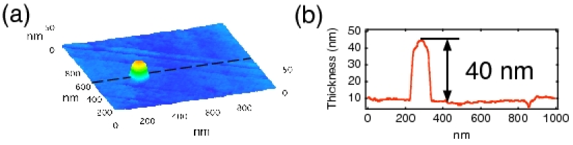
The sample topography was characterized using an atomic force microscope (AFM) in order to evaluate the size and distribution of the diamond nanocrystals. The surface density was of the order of and the typical nanodiamond size was ranging between 30 nm to 100 nm (figure 1).
3 Experimental setup
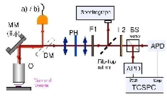
The experimental setup for the optical measurements of the single nickel-nitrogen-related colour centres was based on a home-made confocal microscope (figure 2). The excitation laser, being either a tunable cw Ti:Sa laser or a picosecond pulsed laser emitting at 765 nm, was focused on the sample with a metallographic microscope objective (O) of high numerical aperture (, ) which yielded a spot size of about m. By driving a piezo-electric transducer-mounted mirror (MM), the objective allowed for an raster scan of the sample. Focused was obtained by translating the microscope objective with another piezoelectric transducer.
The same microscope objective also collected the photoluminescence from the colour centres which was then passed through a dichroic mirror (DM) and optical filters (F and F) that removed any residual excitation light. Proper spatial filtering was obtained by focusing in a pinhole (PH). The transmitted photoluminescent light was sent to the detection arms for spectral characterization and assessment of the emitter unicity by the observation of antibunching using a standard Hanbury Brown and Twiss (HBT) setup for photon correlation measurements [29, 30].
4 Continous-wave excitation
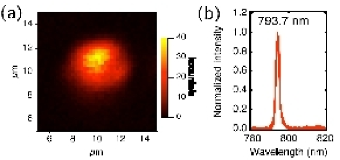
A raster scan over a photoluminescent nanodiamond is shown in figure 3(a). The bright spot gave rise to a sharp spectral emission line centered at 793.7 nm with a width of 2-nm FWHM, as displayed in figure 3(b). This feature is characteristic of the NE8 nickel-nitrogen colour centre [25]. The atomic structure of this point defect was suggested to consist of a nickel atom located at equal distance of two carbon vacancies and associated to four nitrogen impurity atoms in its first coordination shell [31].
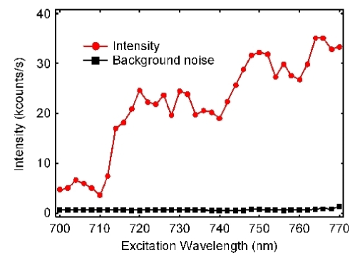
Photoluminescence of this NE8 colour centre was then recorded as a function of the cw excitation wavelength, tuned from 700 nm to 770 nm. Both the position and the shape of the emission line at nm remained identical. As shown in figure 4, the photoluminescence intensity increased with the excitation wavelength while the background level remained constant except for a small increase when the excitation wavelength reached the cutoff edge of the long-pass filter F1. The highest signal-to-background ratio of was achieved for a 765 nm excitation wavelength, which corresponds to a second-harmonic frequency of the telecom band.
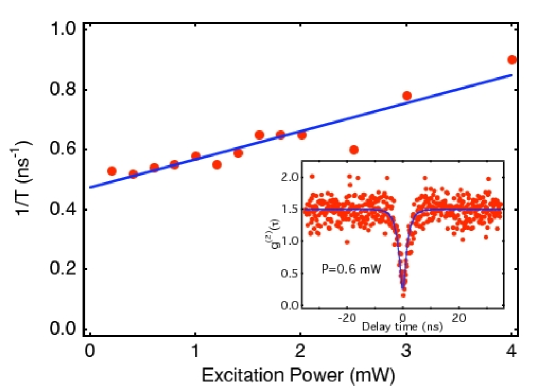
The HBT setup records the histogram of the time separation between successive photodetection events. For our operating conditions and at the limit of short time scale, this histogram is equivalent to a measurement of the normally-ordered intensity autocorrelation function . As shown in the inset of figure 5, a distinct minimum at zero delay, corresponding to , is observed. This indicates that the addressed colour centre was indeed a single emitter. As explained in Ref. [19], fits of recorded with increasing excitation powers yield the evolution of the exponential decay time of the emitter as it gets more and more saturated (figure 5). The extrapolated value for a null excitation intensity allows one to infer an emission lifetime of approximately 2 ns. This value is similar to the one that has been previously measured for individual nickel-nitrogen-related colour centres in a type II-a natural diamond sample [19].
5 Pulsed excitation
The pulsed excitation starts from a mode-locked Erbium-doped fibre laser (PriTel, USA). The laser output, at a wavelength of 1530 nm and emitting a train of a 6.1 ps pulses with a 20 MHz repetition rate, is then amplified in a fiber amplifier and frequency doubled in a periodically-poled lithium niobate crystal. We then obtained picosecond pulses of energy 0.75 nJ at the optimized wavelength of 765 nm.
The TCSPC unit previously used to record the intensity autocorrelation function in the cw excitation regime was employed to measure the histogram of time delays between the laser pulses that trigger the colour centre photoluminescence and the corresponding photon detection events. An exponential decay fit yields an emission lifetime of 2.1 ns, in agreement with the value inferred from the antibunching curves recorded under cw excitation for the same wavelength (see figure 5).
The intensity autocorrelation function is then measured under this pulsed excitation regime and compared to equivalent classical light pulses with Poissonian photon number statistics. Figure 6 shows the corresponding data for the triggered emission of the single NE8 defect and for the attenuated laser pulses, with peaks separated by the excitation repetition period of [32]. In the case of the single NE8 defect, the peak at has almost disappeared which implies that the probability of having two photons in the same output pulse is greatly reduced compared to the equivalent Poissonian statistics.
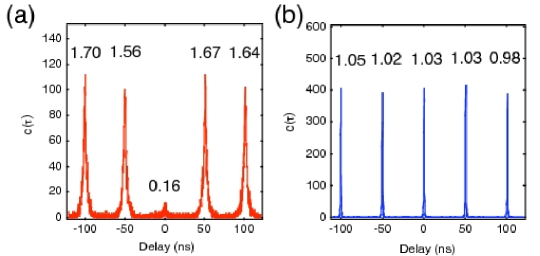
To estimate the quality of the single-photon source, we then quantified this reduction following a procedure described in Ref. [4]. The total number of coincidence counts associated to peak is normalized as:
| (1) |
where and are the counting rates at the output of the two detectors of the HBT setup and is the acquisition time during which the temporal correlation histogram has been recorded.
The normalized value for each peak is indicated in figures 6(a) and 6(b). For attenuated pulses from the excitation laser, is equal to unity within the measurement uncertainty, as it is expected for Poissonian photon number fluctuations. For the single NE8 colour centre emission, the peak at corresponds to , well below unity. The difference between the null value that would correspond to an ideal single-photon source is attributed to a lower signal-to-background ratio observed under pulsed excitation compared to the one measured under cw excitation (see figure 3).
Figure 6(a) also shows that the peaks corresponding to are associated to a value larger than unity. This is attributed to the existence of a “dark” metastable state which is also responsible for the bunching effect observed in the photon correlation measurement under cw excitation. This bunching corresponds to a limit value of higher than unity when exceeds the characteristic decay time (see the inset of figure 5) [19]. Using a model that accounts for random on/off emission [33], the normalized total number of coincidence counts for peak is given by:
| (2) |
where is the mean duration during which the emitter is active and the mean duration during which it is trapped in the dark state and its emission turned off. Fits of the values give and for an average excitation power of focused on the sample.
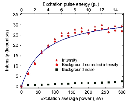
These values can be used to estimate the overall efficiency of the single-photon source. The rate of total detection counts as a function of the average excitation power is shown in figure 7 and can be fitted by
| (3) |
where is the saturation average excitation power and is the rate of detection counts at the limit of saturated emission. Fit of the excitation saturation curve shown in figure 7 yields kcounts/s and W. Taking into account the quantum efficiency of the emitter resulting from parameters and and the overall detection efficiency of the setup, the saturated counting rate can also be estimated by:
| (4) |
The inferred value of this parameter allows us to estimate the detection efficiency for the single NE8 colour centre in a CVD diamond nanocrystal. This value is three times larger than the one previously estimated for the emission of nickel-nitrogen-related colour centres in a bulk diamond sample [19]. The improvement in the collection efficiency is attributed to the sub-wavelength size of the nanocrystal structure.
Conclusion
NE8 nickel-nitrogen colour centers were observed in CVD-grown diamond nanocrystals. Optimization of the CVD growth technique lead to well separated nanocrystals, in which we could observe single colour centers with a high signal-to-background ratio. The photoluminescence dynamics of NE8 colour centers, previously studied in bulk samples, was demonstrated to scale down to these nanosize structures. Moreover, a higher single-photon detection efficiency compared to the previously reported value in bulk diamond [19] was achieved by avoiding the influence of the high index of refraction of diamond.
Both cw and pulsed excitations were used for single-photon emission by these NE8 colour centers. A triggered single-photon source was realized emitting in the nm transmission window. We determined the optimal pulsed excitation wavelength according to the excitation spectrum recorded in the cw regime for a single emitter.
We now plan to increase the triggered single-photon emission rate by growing nanodiamonds on optimized photonic structures, and to implement this single-photon source in an open-air QKD testbed.
References
References
- [1] P. Grangier, B. Sanders, and J. Vuković editors, “Focus on Single Photons on Demand”, New J. Phys. 6 (2004).
- [2] C.H. Bennett and G. Brassard, “Quantum Cryptography: public key distribution and coin tossing”, Proceedings of the IEEE International Conference on Computers, Systems & Signal Processing, pages 175-179, Bangalore (India) (1984).
- [3] N. Lütkenhaus, “Estimates for practical quantum cryptography”, Phys. Rev. A 59, 3301 3320 (1999).
- [4] A. Beveratos, S. Khn, R. Brouri, T. Gacoin, J.-P. Poizat, and P. Grangier, “Room temperature stable single-photon source”, Eur. Phys. J. D 18, 191 (2002).
- [5] E. Waks, K Inoue, C. Santori, D. Fattal, J. Vučović, G.S. Solomon and Y. Yamamoto, Nature 420, 762 (2002).
- [6] A. Beveratos, R. Brouri, T. Gacoin, A. Villing, J.-P. Poizat, and P. Grangier, “Single photon quantum cryptography”, Phys. Rev. Lett. 89, 187901 (2002).
- [7] R. Allaume, F. Treussart, G. Messin, Y. Dumeige, J.-F. Roch, A. Beveratos, R. Brouri-Tualle, J.-P. Poizat, and P. Grangier, “Experimental open-air quantum key distribution with asingle-photon source”, New J. Phys. 6, 92 (2004).
- [8] R. Alléaume, J.-F. Roch, D. Subacius, A. Zavriyev, and A. Trifonov, “Fiber-optics quantum cryptography with single photons”, AIP Conference Proceedings 734, 287 290 (2004).
- [9] A. Soujaeff, T. Nishioka, T. Hasegawa, S. Takeuchi, T. Tsurumaru, K. Sasaki, and M. Matsui, “Quantum key distribution at 1550 nm using a pulse heralded single photon source”, Opt. Exp. 15, 726 (2007).
- [10] V. Scarani, A. Acín, G. Ribordy and N. Gisin,“Quantum cryptography protocols robust against photon number splitting attacks for weak laser pulse implementations”, Phys. Rev. Lett. 92, 0579014 (2004).
- [11] K. Inoue and T. Honjo, “Robustness of differential-phase-shift quantum key distribution against photon-number- splitting attack”, Phys. Rev. A 71, 042305 (2005).
- [12] H.-K. Lo and X. Ma and K. Chen, “Decoy state quantum key distribution”, Phys. Rev. Lett. 94, 230504 (2005).
- [13] Q. Wang, X.-B. Wang, G. Björk, and A. Karlsson, “Improved practical decoy state method in quantum key distribution with parametric down-conversion source”, Europhys. Lett. 79, 40001(2007).
- [14] T. Horikiri and T. Kobayashi, “Decoy state quantum key distribution with a photon number resolved heralded single photon source”, Phys. Rev. A 73, 03233 (2006).
- [15] V. Jacques, E Wu, F. Grosshans, F. Treussart, P. Grangier, A. Aspect, and J.-F. Roch, “Experimental realization of Wheeler’s delayed-choice gedanken experiment”, Science 315, 966 (2007).
- [16] A. Yelisseyev, S. Lawson, I. Sildos, A. Osvet, V. Nadolinny, B. Feigelson, J. M. Baker, M. Newton, and O. Yuryeva, “Effect of HPHT annealing on the photoluminescence of synthetic diamonds grown in the Fe-Ni-C system”, Diamond and Relat. Mater. 12, 2147 (2003).
- [17] K. Johnston and A. Mainwood, “Properties of nickel nitrogen complexes in diamond: stability and electronic structure”, Diamond and Relat. Mater. 12, 516 (2003).
- [18] T. Gaebel, I. Popa, A. Gruber, M. Domhan, F. Jelezko, and J. Wrachtrup, “Stable single-photon source in the near infrared”, New J. Phys. 6 98, (2004).
- [19] E Wu, V. Jacques, F. Treussart, H. Zeng, P. Grangier, and J.-F. Roch, “Narrow band single photon emission in the near infrared for quantum key distribution”, Opt. Exp. 14, 1296 (2006).
- [20] A. Beveratos, R. Brouri, T. Gacoin, J.-P. Poizat, and P. Grangier, “Nonclassical radiation from diamond nanocrystals”, Phys. Rev. A 64, 061802 (2001).
- [21] J. Rabeau, Y. Chin, S. Prawer, F. Jelezko, T. Gaebel, and J. Wrachtrup, “Fabrication of single nickel-nitrogen defects in diamond by chemical vapor deposition”, Appl. Phys. Lett. 86, 131926 (2005).
- [22] J.R. Rabeau, A. Stacey, A. Rabeau, F. Jelezko, I. Mirza, J. Wrachtrup, and S. Prawer, “Single nitrogen vacancy centers in chemical vapor deposited diamond nanocrystals”, Nano Lett., ASAP Article 10.1021/nl0719271 S1530-6984(07)01927-3, e-print: cond-mat/arXiv:0706.2518 (2007).
- [23] J. R. Rabeau, S. T. Huntington, A. D. Greentree, and S. Prawer, “Diamond chemical-vapor deposition on optical fibers for fluorescence waveguiding”, Appl. Phys. Lett. 86, 134104 (2005).
- [24] C.F. Wang, Y-S. Choi, J.C. Lee, E.L. Hu, J. Yang, and J.E. Butler , “Observation of whispering gallery modes in nanocrystalline diamond microdisks”, Appl. Phys. Lett. 90, 081110 (2007).
- [25] A.M. Zaitsev, Optical properties of diamond, A Data Handbook (Springer, 2000).
- [26] Y. Dumeige, F. Treussart, R. Alléaume, T. Gacoin, J.-F. Roch, P. Grangier, “Photo-induced creation of nitrogen-related color centers in diamond nanocrystals under femtosecond illumination”, J. Lumin. 109, 61-67 (2004).
- [27] E. Rohrer, C.F.O. Graeff, R. Janssen, C.E. Nebel, M. Stutzmann, H. Gttler, and R. Zachai, “Nitrogen-related dopant and defect states in CVD diamond”, Phys. Rev. B 54, 7874 (1996).
- [28] Y. Lifshitz, C. H. Lee, Y. Wu, W. J. Zhang, I. Bello, and S. T. Lee, “Role of nucleation in nanodiamond film growth”, Appl. Phys. Lett. 88, 243114 (2006).
- [29] R. Brouri, A. Beveratos, J.-P. Poizat, and P. Grangier, “Photon antibunching in the fluorescence of individual color centers in diamond”, Opt. Lett. 25, 1294 (2000).
- [30] C. Kurtsiefer, S. Mayer, P. Zarda, and H. Weinfurter, “Stable solid-state source of single photons”, Phys. Rev. Lett. 85, 290 (2000).
- [31] A. Nadolinny, A. P. Yelisseyev, J. M. Baker, M. E. Newton, D. J. Twitchen, S. C. Lawson, O. P. Yuryeva and B. N. Feigelson, “A study of 13C hyperfine structure in the EPR of nickel-nitrogen-containing centres in diamond and correlation with their optical properties”, J. Phys: Cond. Mat. 11, 7357 (1999).
- [32] C. Brunel, B. Lounis, P. Tamarat, and M. Orrit, “Triggered source of single photons based on controlled single molecule fluorescence”, Phys. Rev. Lett. 83, 2722 (1999).
- [33] C. Santori, M. Pelton, G. Solomon, Y. Dale, and Y. Yamamoto, “Triggered single photons from a quantum dot”, Phys. Rev. Lett. 86, 1502 (2001).