Biperiodic superlattices and the transparent state
Abstract
We study biperiodic semiconductor superlattices, which consist of alternating cell types, one with wide wells and the other narrow wells, separated by equal strength barriers. If the wells were identical, it would be a simply periodic system of half-cells. When asymmetry is introduced, an allowed band splits at the Bragg point into two disjoint allowed bands. The Bragg resonance turns into a transparent state located close to the band edge of the lower(upper) band when the first(second) well is the wider. Analysis of this system gives insight into how band splitting occurs. Further we consider semi-periodic systems having half-cells. Surprisingly these have very different transmission properties, with an envelope of transmission maxima that crosses the envelope of minima at the transparent point.
pacs:
73.21.Cd, 73.61.Ey 03.65.NkI Introduction
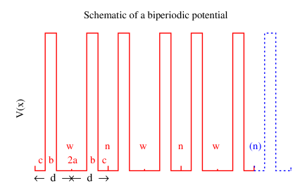
Coquelin et al. Coq1 ; Coq2 carried out experiments on electron transmission through a finite biperiodic GaAs/AlGaAs superlattice consisting of alternating types of unit cells. Biperiodic systems occur naturally in crystals and polymers AC04 , but in layered semiconductor heterostructures one has control over the properties of the cells. As illustrated by the red (solid) line in Fig. 1, Coquelin’s system had identical barriers of width nm, while there are two alternating well widths, nm (wide) and nm (narrow), which changes it from a simply periodic to a biperiodic system.
We will consider the basic unit, called a half-cell, to comprise three layers: two well segments of GaAs having widths separated by an AlGaAs barrier of width . A full or “double-cell” consists of a half-cell plus another which is its mirror image. The double-cell of width centered on the origin, is marked in Fig. 1 at the left of the three-cell array, in red. It has layers of widths and is overall reflection symmetric about its mid-point. Due to the two barriers enclosing a well of width , there will be quasi-bound states which show up as resonances in electron scattering from the double cell. When such cells are juxtaposed, the wells will be alternately wide and narrow; hence the name biperiodic array. Each double cell is a symmetric cell, and the complete array has reflection symmetry. By exchanging the values of and , the character of the array will change from say to , where and stand for wide and narrow wells respectively.
The experimental device Coq1 ; Coq2 had double cells, so there were wells enclosed between barriers. This number was chosen because it provides enough separation between the measured transmission resonances for them to be distinguished. When , the simply periodic system of symmetric cells is known FPP ; CP81 ; PC82 ; VC86 ; YKT89 ; KL92 ; KL95 ; BDS96 ; Gom99 ; Yang00 ; GS01 ; SYR02 ; PP05 ; GK03 ; YMS02 ; MYS02 ; SD02 to exhibit transmission resonances in each allowed band, according to
| (1) |
where is the Bloch phase of the half-cell, and is its impedance parameter in the Kard parameterization Eq. (10) of the transfer matrixSMM03 ; SMM04 . The fundamental band structure depends on those properties of the half-cell, while the width and spacing of individual resonances depends on the number of half-cells, via , with .
When , the half-cell is asymmetric under reflection, though the double cell remains symmetric. Each allowed band develops a band gap near the Bragg point . An allowed band of the double-cell system should show two resonances. As is seen in Fig. 2, one of the allowed bands contains a third resonance which we will identify as a transparent state at which the impedance parameter , causing the envelope of minimum transmission probability to be pushed up to unity. Such a state occurs at a fixed energy, independent of the number of double cells included, as can be seen from eq. 1. This transparent state lies very close to a band edge, in the lower (upper) split band when the wide (narrow) well is first in line for incident electrons.
The purpose of this paper is to explain why and how the transparent state arises when the half-cell becomes asymmetric, and why it is located very close to the split band edge. In Sec. IV we will consider the surprising effect of including an additional half cell, as suggested by the dashed blue line at the right in Fig. 1.
II Transfer matrix analysis
II.1 General
We will follow the line of argument of Shockley Surf , who studied surface states of a finite static periodic potential whose unit cell is symmetric about its mid-point. We extend his method to allow for the position and energy-dependent effective mass, required in a semiconductor superlattice. Since the full cell has reflection symmetry, it is sufficient to solve the Schrödinger equation for the half-cell . The even () and odd () parity solutions take the boundary values and at the origin. [Note: Following the development of Appendix A, the prime means take the derivative, and then divide by the variable factor to allow for the effective mass, , which is dimensionless.] The transfer matrix for the half-cell is
| (2) |
where the wave functions without argument are always evaluated at the point . Placing the half-cells in reverse order, simply interchanges the elements and .
Since the Wronskian of two solutions is a constant, . In dealing with a constant potential and constant , for example, one has
| (3) |
which are chosen so that at (well bottom), we have solutions and .
For the symmetric double cell , the transfer matrix is
| (4) | |||||
To transform to the ingoing/outgoing waves representation we proceed as in Appendix A with as the velocity outside the potential. Unlike , the matrix operates from right to left. For the full cell it is given by eq. 26.
| a) |  |
|---|---|
| b) |  |
Shockley’s first step was to derive the Bloch phase of the double cell in terms of the solutions of the half cell, by appealing to Floquet’s theorem. He obtained
| (5) |
where are the log-derivatives of the half-cell solutions respectively. One finds easily that
| (6) |
where the denominator is . We write in the parameterized form
| (7) |
The log-derivatives determine the effective velocity and the Bloch phase at each energy, for a symmetric double cell. Again, in case of a constant potential across the cell, they would be
| (8) |
It is evident that in an allowed band and must have opposite signs, to make both and real. Conversely in a forbidden band and have the same sign.
II.2 Asymmetric delta-barrier cells
To gain insight into how band splitting occurs, we consider a simple model which replaces the square barrier cells illustrated in Fig. 1 by delta-function barriers of strength , (a value chosen to give results similar to those of the Coquelin potential Coq1 ). In the well sections, we have (see Eqs. (A3, A5)).The transfer matrix for a half-cell of width is
| (11) |
We have written ; is the asymmetry. The double-cell has two barriers and a well of width between. Reversing the sign of interchanges and , which is equivalent to putting the two half-cells in the opposite order. When a wide well occurs on both ends of the biperiodic superlattice.
The band structure depends only on the location of the zeroes and poles of . These locations do not change if the in front of the off-diagonal elements and is multiplied by a constant factor. To reduce the number of parameters in play, we replace that , equivalent to saying that . Then the transfer matrix of the delta-barrier model is a function of dimensionless variables , and . The figures are drawn as functions of ; the lowest allowed band ends when .
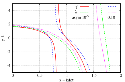
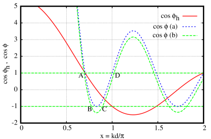
Figure 3 shows the evolution of the log-derivatives and versus , for two values of the asymmetry parameter, , and . For a fixed cell width , the plot shows the energy dependence (via ). Larger moves the poles to the left, seen by the red and blue lines for . For (green and mauve lines) the node shifts to the right. Allowed bands occur when and have opposite signs, which covers much of the interval for between and . For the asymmetry, the pole of at approximately almost coincides with a node of , creating an infinitesimal forbidden band there. For a reflection symmetric half-cell, they would exactly coincide, and cancel, giving a vanishing gap. For the larger asymmetry, the separation between the pole and node increases, widening the gap. A magnified view of this region is shown in Fig. 6.
In Fig. 4 we see the corresponding Bloch phases. The red (solid) lines are the of the half cell, while the blue (dotted) and green (dashed) lines are the of the double cell. For line (a) the angle is almost equal to , so when , the dashed line scarcely descends below . However, for moderate asymmetry (line(b)), the undershoot is evident, and a sizeable band gap opens up between (B) and (C). The outer band edges, marked by and , shift outwards a little at the same time.
In Fig. 5, the green (long dashed) line is ; positive values are necessary for an allowed band to exist. The solid line is defined in eq. 7. The short dashed line is the alternative value , which results when we interchange the values of and , choosing the opposite asymmetry. Since this changes the sign of , it is equivalent to interchanging the values of and , which leaves the trace of and therefore unchanged. In panel (a) lies almost on top of , because the asymmetry is practically zero; only a small glitch (due to finite steps in drawing) marks the location on the curve near . In panel (b) the poles of and separate cleanly. When , is large below the band gap, and small above the band gap, which runs from to . When , applies and those properties reverse.
The two panels of Fig. 6 provide a magnified view of the split band region. The straight mauve (dotted) and black (double-dash) lines are multiples of and , the negative sign imposed so that their crossing point can be easily identified. This is the point at which Tr, which makes . For a symmetric half-cell, this is the energy where the pole and node coincide, and cancel each other. The point labelled B is a node of and a pole of , at the lower edge of the band gap. To the left of the pole, (red, solid) diverges, and so does . Since rises though all positive values between threshold at A and the pole at B, at some point it must equal the external velocity , which makes the impedance parameter . That defines the transparent point, at which independent of the number of cells or the value of the Bloch phase. This accounts for the third transmission resonance in the lower allowed band of Fig. 2(a). Conversely, if we take the opposite asymmetry, (so the narrow well is first in line), then it is the alternate function which applies. This pole has the opposite sign residue, so it is the divergence of near point labelled C at the lower edge of the upper allowed band, which produces the transparent state.
In Fig. 6(a), the two poles are very close together at BC. In the limit of exact reflection symmetry, they would coincide, and their sum would be zero. The band gap would disappear, and would touch without crossing below that line.
| a) | 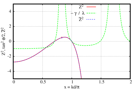 |
|---|---|
| b) | 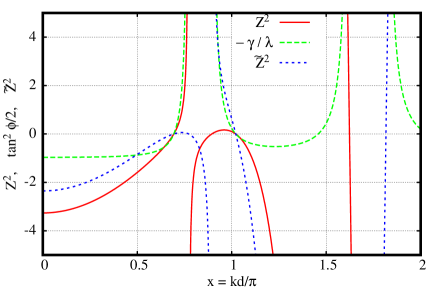 |
III General case
To discuss the general case of barrier-type cells arranged from left to right in order , we write the transfer matrices (in an allowed band) in terms of three real parameters as follows:
| (12) |
Comparing to of eq. 7, we see that , half the Bloch phase of the symmetric double cell, while is the corresponding velocity parameter. Interchanging the half-cells is equivalent to reversing the sign of , which measures the degree of asymmetry of the half-cell, but leaving and unchanged. Incrementing the number of half-cells leads to the following rule:
| (13) |
| a) | 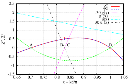 |
|---|---|
| b) | 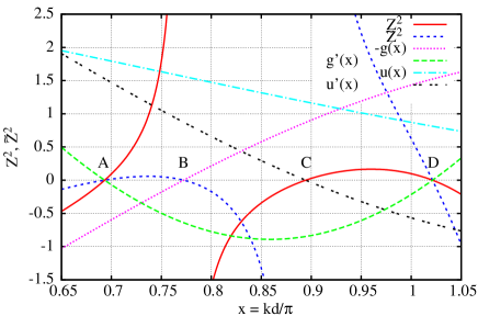 |
The number can be replaced by any odd integer, and by any even integer. When the index is even the system has reflection symmetry and , but appears on the off-diagonal elements making . For odd orders , the transfer matrix is modelled on the half-cell, (here ), which is repeated one extra time. Then
| (14) |
Superlattices with an odd number of half-cells are biperiodic but not reflection symmetric. They exist in two forms depending on the sign of , (or what is the same thing, whether the first well on the left is of wide or narrow type). We will discuss their surprising properties below; for now we concentrate on the case which are symmetric biperiodic systems involving double-cells.
| a) |  |
|---|---|
| b) |  |
| c) |  |
IV Transmission in symmetric biperiodic systems
The transmission probabilities shown in Fig. 2 were calculated for the system described in the first paper of Coquelin et al. Coq1 . We took into account the variable effective mass and other material properties as in PG03 ; MPG03 ; PBG05 . Specifically, the barrier height is 288.09 meV, and the effective masses are approximately 0.074 (well) and 0.080 (barrier).
Results shown in Figs. 2 (a) and (b) correspond to the two devices with ‘wnwnw’ and ‘nwnwn’ well arrays. The total width of the allowed bands is the same for both cases because the Bloch phase of the double cell is the same for both orderingsPG03 . What is different between the two cases is the impedance parameter ; this accounts for the different results obtained. In Fig. 2(a) the lower allowed band runs from 92 to 97.5 meV. The long dashed line is the envelope of minimum transmission, the curve : see eq. 1. The presence of the transparent state with just inside the allowed band, pushes the envelope of minima up to unity. This is the cause of the third resonance sitting close to the band edge; its width is driven by the envelope of minima. The envelope (dashed line) is continued across the forbidden band, (where it has other significance,) but it is seen to decay slowly across the forbidden zone, and is very low in the second allowed band. In panel (b), the order of the half-cells is reversed, and the extra state occurs in the upper band.
It is impressive that even a small departure from strict periodicity has such a large effect on the band structure, opening a sizeable gap from 98. to 112. meV, while narrowing the allowed band width as compared to the case of all wide or all narrow wells. The difference between the 3.8 and 4.3 nm widths is only 13%. Since and are single-cell properties, increasing the number of cells has no effect on the band structure; it simply squeezes more resonances into the bands. In a forbidden zone, . Since increases rapidly above 98 meV, the transmission does cut off sharply in the forbidden zone, even for just three double-cells.
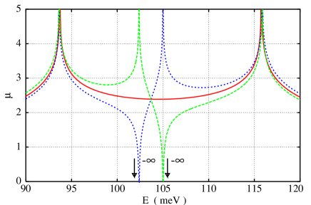
Further insight is gained by looking at a sequence of models very close to the symmetric () limit. In Fig. 7(a) we start with a simply periodic system using wells of the average width 4.05 nm. Then we made a small excursion into asymmetry by using and nm for the wide and narrow wells respectively. In Fig. 7(b) it is the configuration and in panel (c) the . The gap induced is about 2.6 meV, while the outer band edges are little shifted.
The transparent state clearly develops from the Bragg state of the symmetric double-cell, at meV. The double cell has strong barriers, so the energies of its quasibound states are determined primarily by the well width SJW00 . When asymmetry is introduced, , in the notation of eq. 11. The energy difference of the two cases, wide or narrow well, is therefore of order meV, in Fig. 2. This agrees well with the locations of the transparent states at 97.4 and 110.5 meV, when nm and nm. In Fig. 7, nm and the splitting is 2.6 meV. In a tight-binding model, the transparent state is an edge state of one of the split bands, in which only the wide or only the narrow wells are occupied at resonance, which is consistent with the quasibound state picture.
In Fig. 8, the impedance parameters of the three situations are drawn. The red (solid) line exhibits typical behaviour SMM04 with a divergence of at the band edges. In blue (dotted) the band splitting has caused to descend steeply through zero at the transparent state, before diverging to at the band gap edge, meV. In the forbidden band, ; rises from and diverges to at the upper edge of the band gap. The behaviour in the upper allowed band reverts to the typical one. In green (dashed), the negative divergence of is transferred to the lower edge of the upper band. The subsequent rise in the allowed band produces the transparent state and the consequent large values of the envelope of minimum transmission, just above that band edge.
In ref. SMM04 we interpreted the transfer matrix as a mapping of the system point in the complex plane, or as a hyperbolic rotation of a Dirac spinor around a fixed axis whose orientation is determined by . The axis passes through a fixed point at distance from the origin. In the first allowed band of a symmetric system, as a function of energy, the fixed points start and end at at the band edges, moving on the real axis. Then in the forbidden band, two fixed points move around the unit circle in complex conjugate positions, from to . In the ensuing allowed band the motion starts and ends at . The motion which arises here is quite different, in that (in Fig. 8, blue line) the interior fixed point begins at at the lower edge of the first allowed band, but does not return to at the band edge; rather it remains on the real axis and moves through the origin to reach at the lower edge of the gap. Its passage through the origin produces the transparent point. In the band gap, the fixed points do move on the unit circle, initially very quickly to reach and then more slowly reaching at the lower edge of the second allowed band. The fixed points then move on the real axis in the normal manner, starting and ending at in the upper split band. The fixed points must reach at a band edge, so this is perhaps the only way that a new forbidden band can be inserted, without disturbing higher bands.
V Transmission for odd systems
Now we return to the the case of an odd number of half-cells. Since the half-cell already encapsulates the band structure of the symmetric double-cell, it might seem that there is nothing further to learn from considering the addition of an extra factor as in eq. 13. Surprisingly, it changes everything. When we form the -matrix from , we obtain the elements
| (15) | |||||
For any odd number of cells, simply replace leaving the rest unchanged. It is easily checked that det , and putting the extra half-cell on the left, rather than the right, only reverses the sign of .
In comparison, for the double-cell one has
| (16) |
It follows that .
Using of eq. 15 we have
| (17) | |||||
Suppose that , making the factor in square brackets positive. Then from the second line in eq. 17 we get a lower bound on the inverse transmission probability, and from the third line an upper bound. That is,
| (18) |
When , the upper and lower bounds are exchanged. At a point where , (which implies ), the bounds cross, and is caught between them. For a symmetric half-cell, , so the upper bound on transmission reverts to unity, and plays the role of in producing the envelope of minimum transmission for the double cell.
When , transmission reaches the upper bound when , and the lower when . ( and integers.) In the opposite case, , the bounds are reversed, and the upper bound is reached at . At the “transparent” point where , the transmission is pinched between the bounds and takes the value .
| a) | 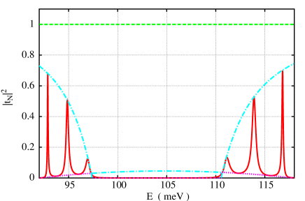 |
|---|---|
| b) | 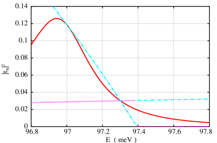 |
Some results are presented in Fig. 9, for the same potential cell used in Fig. 2, appropriate for GaAs/AlGaAs superlattices. To start we take half-cells. Panel (a) shows the transmission in both parts of the split bands, with three resonances in each. One sees that the envelope of maxima, crosses the envelope of minima, , at the transparent point . From there to the band edge, they exchange their roles as upper/lower bounds. The upper bound reduces the maximum transmission by a large amount in comparison to the situation in Fig. 2, which is for six half-cells. In the forbidden band, it can be shown that what was the envelope of mimina becomes an upper bound on transmission, while the lower bound is zero. The cross-over at the transparent point ensures that these bounds are continuous.
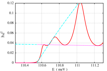
Fig. 9(b) shows detail near the transparent point. Where the bounds cross, is pinched between them. To the left of the transparent point (which it no longer is!), the maxima occur when , with integer . From the third line of eq. 17, any maxima that occur after the transparent point satisfy , with integer . Such a situation must occur for a large enough , because the energy of the transparent point is fixed, while having more cells squeezes additional resonances into each allowed band. In Fig. 10 we show detail of the region near the lower edge of the upper band, for half-cells. Here one of the resonances clearly lies between the band edge and the transparent state.
Innumerable papers have been written on symmetric periodic systems, for which the relation eq. 1 applies, and their resonances always involve perfect transmission. Therefore it is a surprise to see how adding a half-cell introduces a non-trivial upper bound on transmission, greatly reducing it in the neighbourhood of the “transparent” state.
VI Conclusion
We have studied transmission through biperiodic semiconductor superlattices. For an even number of half-cells, asymmetry causes each allowed band to split at the Bragg energy where . Extending Shockley’s line of argument for a generic single-barrier cell, we have proved that this induces a transparent state which lies in one of the split bands, and very close to the band edge. The rule is that the transparent state lies in the lower band when the wide well is first in line for incident electrons. The transparent state is a resonance which occurs at a fixed energy, independent of the number of cells in the array; otherwise the transmission follows the well known rule expressed in eq. 1.
For an odd number of half cells, the picture is completely different. These systems are asymmetric, so if there is a wide well first on the left, there will be a narrow well first from the right. The asymmetry due to the additional half-cell causes an envelope of maximum transmission to appear, which crosses the envelope of minimum transmission at the “transparent” point, in both split bands. The transmission probability is given by eq. 17 and is bounded on both sides as in eq. 18. At the transparent point , the bounds cross, and the transmission probability is pinched between them. Resonances occurring between the transparent state and the band edge satisfy a different rule, , not the which would follow from eq. 1.
In a separate article we will discuss these systems in a tight binding model, showing what can and cannot be reproduced in that approximation. For example, in tight binding, the transparent state occurs exactly at a band edge, rather than just inside.
Acknowledgements.
We are grateful to NSERC-Canada for support under Discovery Grants RGPIN-3198 (DWLS), SAPIN-8672 (WvD) and a Summer Research Award through Redeemer University College (LWAV); also to DGES-Spain for continued support through grants FIS2004-03156 and FIS2006-10268-C03 (JM).Appendix A Transfer matrices
For completeness, we write down our conventions for transfer matrices in the presence of an energy and position-dependent effective mass. The Schrödinger equation is
| (19) | |||||
The dimensionless effective mass (in units of the free electron mass ) is ; is the wave number inside the potential region, and in the exterior region where both and become constant. (In this paper, the substrate and cap of the heterostructure are GaAs, the same as the wells of the superlattice.)
If and are two independent solutions, then
| (20) |
where the constant may be set equal to one by choice of the boundary condition at some initial point, say . For example, take , , and .
The transfer matrix relates values of a “spinor” whose components are and between two points.
| (21) |
The Wronskian relation gives det, and in an allowed band, Tr, where is the Bloch phase. It is easily shown that
| (22) |
The band structure associated with the potential is all contained in the -matrix for a single cell. If we agree that the prime symbol on the wave function means to take the derivative, and then multiply by , all the above equations reduce to the standard form for the case with constant effective mass, in which . (i.e. the effective mass can be absorbed into , or one may use an average value and leave it explicit.)
In discussing transmission properties it is more convenient to represent the wave function in terms of plane wave states, normalized to unit flux. To the left () and right () of the potential we write:
| (23) |
where the external velocity is , with , and similarly for . By definition the transfer matrix relates the plane wave coefficients across the system
| (24) |
Different wave numbers at left and right allow for bias across the potential MSM04 , but here we will not consider that situation further, so that .
Appendix B Kard representation in a forbidden band
The parameterization given in eqs. 12 or 13 is valid in all allowed bands, if we permit all real values for and . In forbidden bands matters are a little more complicated. We discuss here the behaviour of the half-cell matrix , in relation to the bands of the multi-cell system.
We have in mind a half-cell of type well-barrier-well, and the exterior energy is measured from the well-bottom. At zero energy one is in a forbidden zone which we will label (FZ0). All four elements of are positive, as are the ratios and . The allowed zone (AZ0) begins when becomes negative. The parameters are all positive in AZ0, with in the first quadrant. If we change and in FZ0, the correct signs and magnitudes are obtained: see line one of eq. 27.
The band AZ0 ends when also becomes negative, so that the log derivatives are both negative, in FZ1. This in turn ends when becomes negative and the second allowed band AZ1 begins. Eventually again becomes positive, and FZ2 occurs, now with both log-derivatives negative. The signs are summarized in Table 1, for energies up to 305 meV for a GaAs/AlGaAs SL. In AZ1, the diagonal elements are negative, which is accommodated by placing in the second quadrant. Since is still positive, remains positive. Similarly in AZ3, placing in the third quadrant replicates the signs.
In the forbidden zone FZ0, all four elements of are positive. In FZ1, both and are negative. Because at the band edge, the diagonal elements () are smaller in magnitude than the off-diagonal (), so for continuity. The cosh and sinh must change places. This is accomplished by , , and unchanged. The phase increases monotonically through allowed zones, and its real part is stationary in forbidden zones. When acquires a phase, does not. The first few lines of Table 1 summarize these adjustments.
Similarly, in FZ3, the prescription , gives the correct signs. There is ample scope to manoeuvre things to fit whatever pattern of signs arises, but we doubt that there is any general prescription that will fit every possible potential.
| Band | |||||||
| + | + | + | + | ||||
| + | + | + | I | ||||
| + | + | ||||||
| + | II | ||||||
| + | + | ||||||
| + | III | ||||||
| + | + |
Explicit forms for the first four forbidden bands are
| (27) |
Transforming from to (for the half-cell),
In FZ0,
| (29) |
In FZ0 the upper limit on transmission is given by , as in an allowed band. Also, for large , approaches zero, as for periodic systems. In the next forbidden zone FZ1,
| (30) | |||||
The last line of 30 shows that an upper limit on the transmission probability is given by , but there is no lower limit. In Figs. 9 and 10, it can be see that the upper limit in the forbidden zone is the continuation of from the adjacent allowed zone.
The roles of and are exchanged between eqs. 29 and 30. This pattern applies to all FZ with even and odd indexed subscripts.
In FZ2, the expressions for and are the complex conjugates of those in eq. 29, and in FZ3 they are complex conjugates of those in eq. 30. This pattern appears to persist in going to higher bands, but may depend on the detailed form of the potential. The forbidden zones with even and odd labels have different patterns, due to the need to exchange the roles of and in the latter case.
The main virtue of the Kard parameterization is that, in allowed bands, it makes the relations between the single and multiple cell systems very obvious. Kard is less convenient in forbidden bands, but with sufficient care it offers the same advantages.
References
- (1) M. Coquelin, C. Pacher, M. Kast, G. Strasser and E. Gornik, “Transport studies on doubly periodic superlattices by hot electron spectroscopy”. Contribution P-154 to Int. Conf. Phys. of Semiconductors, Edinburgh (2002). Published on CD in IOP Conference Series, Vol. 171, eds. A R Long and J H Davies, (2003) ISBN:-7503-0924-5
- (2) M. Coquelin, C. Pacher, M. Kast, G. Strasser and E. Gornik, “Wannier-Stark level anti-crossing in biperiodic superlattices”, Physica Stat. Sol. B 243 (2006) 3692-5.
- (3) Polaritons in periodic and quasiperiodic structures, E.L. Albuquerque and M.G. Cottam, Elsevier, (Amsterdam, 2004), ISBN = 044516271.
- (4) D.W.L. Sprung, Hua Wu and J. Martorell, “Scattering by a finite periodic potential”, Am. J. Phys. 61 (1993) 1118-24.
- (5) M. Cvetič and L. Pičman, “Scattering states for a finite chain in one dimension”, J. Phys. A: Mathematical and General, 14 (1981) 379-382.
- (6) M. Pacheco and F. Claro, “Simple results for one-dimensional potential models”, Phys. Stat. Sol. B, 114 (1982) 399-403.
- (7) D.J. Vezzetti and M.M. Cahay, “Transmission resonances in finite, repeated structures”, J. Phys. D: Applied Physics, 19 (1986) L53-L55.
- (8) H. Yamamoto, Y. Kanie and K. Taniguchi, “Transmission and resonance condition in n-fold barrier structures”, Phys. Stat. Sol. B, 154 (1989) 195-199.
- (9) T.M. Kalotas and A.R. Lee, “Solution of Schrödinger’s equation for 1D finite-range potentials” Physica Scripta 45 (1992) 552-9.
- (10) T.M. Kalotas and A.R. Lee, “The spectra of periodic potentials in finite boxes”, Euro. J. Phys. 16 (1995) 119-23, and references therein.
- (11) J.M. Bendickson, J.P. Dowling and M. Scalora, “Electromagnetic mode density in finite, 1D photonic band-gap structures ”, Phys. Rev. E 53 (1996) 4107-21.
- (12) I. Gomez, F. Dominguez-Adame, E. Diez, & V. Bellani, “Electron transport across a gaussian superlattice”, J. Appl. Phys. 85 (1999) 3916.
- (13) Q.K. Yang and A.Z. Li, “Energy filters using modulated superlattices”, J. Appl. Phys. 87 (2000) 1963-7.
- (14) D.J. Griffiths and C.A. Steinke, “Waves in locally periodic media”, Am. J. Phys. 69 (2001) 137-154.
- (15) Shang Yuan Ren, “Two types of states in 1D crystals of finite length”, Ann. Phys. (NY) 301 (2002) 22-30.
- (16) Pedro Pereyra, “Eigenvalues, eigenfunctions and surface states in FPP”, Ann. Phys. (NY) 320 (2005) 1-20.
- (17) E. Georgieva and Y. S. Kim, “Iwasawa effects in multilayer optics”, Phys. Rev. E 64 (2001) 026602
- (18) T. Yonte, J.J. Monzón, L.L. Sánchez-Soto, J.F. Cariñena and C. López-Lacasta, J. Opt. Soc. Am. A 19 (2002) 603.
- (19) J.J. Monzón, T. Yonte, L.L. Sánchez-Soto, and J.F. Cariñena, J. Opt. Soc. Am. A 19 (2002) 985.
- (20) Maria Stȩślicka, R. Kucharczyk, A. Akjouj, B. Djafari-Rouhani, L. Dobrzynski & S.G. Davison, “Localised electronic states in semiconductor superlattices”, Surf. Sci. Rep. 47 (2002) 93-196.
- (21) D.W.L. Sprung, G.V. Morozov and J. Martorell, “Anti-reflection coatings from the analogy between electron scattering and spin precession”, J. App. Phys. 93 (2003) 4395-4406.
- (22) D.W.L. Sprung, G.V. Morozov and J. Martorell, “Geometrical approach to scattering in one dimension”, J. Phys. A, 37 (2004) 1861-80; Corrigendum ibid. 40 (2007) 6001.
- (23) W. Shockley, Phys. Rev. 56 (1939) 317-323.
- (24) C. Pacher and E. Gornik, “Adjusting coherent transport in finite periodic superlattices”, Phys. Rev. B 68 (2003) 155319, 9pp.
- (25) U. Merc, C. Pacher, M. Topic, F. Smole, E. Gornik, “Electron velocity in superlattices”, Euro. Phys. J. B 35 (2003) 443-447.
- (26) C. Pacher, W. Boxleitner & E. Gornik, “Coherent resonant tunneling time and velocity in finite periodic systems”, Phys. Rev. B 71 (2005) 125317, 11 pp.
- (27) D.W.L. Sprung, J. D. Sigetich, Hua Wu and J. Martorell, “Bound states of a finite periodic potential”, Am. J. Phys. 68 (2000) 715-22.
- (28) J. Martorell, D.W.L. Sprung and G.V. Morozov, “Electron band-pass filters for biased finite superlattices”, Phys. Rev. B 69 (2004) 115309, 10 pp.