On-Chip Matching Networks for Radio-Frequency Single-Electron-Transistors
Abstract
In this letter, we describe operation of a radio-frequency superconducting single electron transistor (RF-SSET) with an on-chip superconducting matching network consisting of a spiral inductor and its capacitance to ground . The superconducting network has a lower and gives a better matching for the RF-SSET than does a commercial chip inductor. Moreover, the superconducting network has negligibly low dissipation, leading to sensitive response to changes in the RF-SSET impedance. The charge sensitivity in the sub-gap region and energy sensitivity indicate that the RF-SSET is operating in the vicinity of the shot noise limit.
With growing interest in quantum computation,Shor (1994); Grover (1997) spin-based qubits,Elzerman et al. (2004); Petta et al. (2005) the quantum properties of nanomechanical resonators,Knobel and Cleland (2003); LaHaye et al. (2004) and quantum measurementBraginsky and Khalili (1992); Devoret and Schoelkopf (2000) much attention has been focused on ultra-fast charge detectors such as the radio-frequency single electron transistor (RF-SET).Schoelkopf et al. (1998); Aassime et al. (2001a, b); Brenning et al. (2006) In rf mode, the SET is embedded in an network as illustrated in Fig. 1(a) allowing a working bandwidth of tens of MHz and avoiding noise from amplifiers and background charges. The network usually consists of a commercial chip inductor and its parasitic capacitance to ground ; such networks, however, have drawbacks such as losses and relatively large that degrade the performance of the SET. In this letter, we describe RF-SSETs with on-chip fully superconducting matching networks. Although our best charge sensitivity does not quite match the record to dateBrenning et al. (2006), our SET and matching network design are not yet fully optimized. Furthermore, our measurement is in the sub-gap region for which transport occurs via a combination of Cooper pair and quasiparticle tunneling. The backaction of the SET, the rate at which it dephases a measurement,Clerk et al. (2002); Makhlin et al. (2001) is predicted to be smaller in the sub-gap region than in the above-gap region for which Coulomb blockade of quasiparticles dominates.Aassime et al. (2001a, b); Brenning et al. (2006)
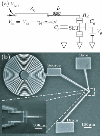
Fig. 1(a) shows an idealized model for an on-chip superconducting matching network. One end of the SET is connected to an Al spiral inductor , which is then connected via a coaxial cable to room temperature electronics. The other end of the SET is grounded directly to the cable shield. The inductor , the SET differential resistance , and the stray capacitance from the inductor and SET bonding pads to ground form an network with resonant frequency . A carrier wave with frequency and rms amplitude is applied to the network and the reflected signal is measured. The reflection coefficient at resonance is given by where the input impedance of the network . In order to optimize the charge sensitivity, should be impedance matched to the coaxial cable at the point of maximal change in SET conductance with charge. The unloaded quality factor determines the amplitude of the rf signal applied to the SET and the resonance bandwidth .
An on-chip superconducting matching network has three advantages in comparison with a commercial chip inductor. First, because is smaller for an on-chip network, better impedance matching can be attained at higher frequencies, resulting in a larger resonance bandwidth for a given . Second, an on-chip network can be extended to multi-pole matching networksAbrie (2000) that can further increase the bandwidth, possibly allowing measurements on nanosecond time scales. Finally, our on-chip networks are entirely superconducting at our measurement temperature and have negligible loss at radio frequencies. In comparison, the input impedance at resonance of a matching network that includes normal metals has loss terms arising from dissipation in the inductor or capacitor in addition to the transformed SET impedance . The reflection coefficient for a lossy network is therefore less sensitive to changes in . While fully on-chip matching networks have been used previously, they have generally included some normal metal components.Stevenson et al. (2002); LaHaye et al. (2004)
Fig. 1(b) shows an optical micrograph of an on-chip network. The network is fabricated together with the SET by e-beam lithography and double-angle shadow evaporation of Al. The number and spacing of the turns of the spiral inductor (linewidth , line spacing ) determines . The inset of Fig. 1(b) shows a scanning electron micrograph of the SET with junction area about 4060 . The center of the spiral inductor is wire bonded using an Al wire to the central pin of a coaxial cable and the ground lead of the SET is similarly bonded to the cable shield.
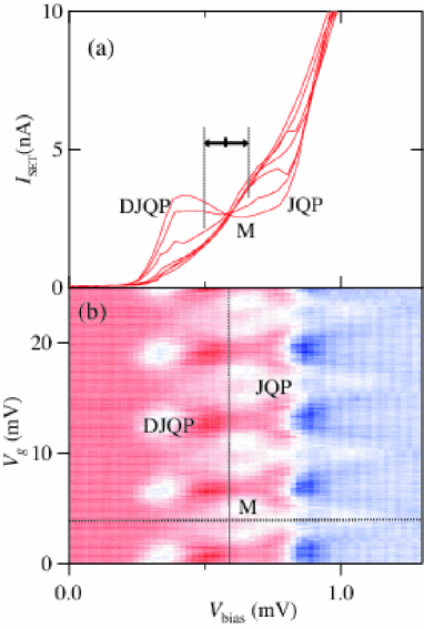
The measurements were carried out in a 3He refrigerator at the base temperature of . Copper-stainless steel powder filters in the cryostat and -type filters at room temperature were used to eliminate high frequency noise. A low-noise HEMT amplifier and directional coupler were located in the cryostat at a temperature of around . We made two samples with the same SET design and similar total normal-state resistance : sample A was coupled to a 12-turn spiral inductor and sample B to a 14-turn inductor. DC - curves were measured with custom-made low noise current and voltage amplifiers, and the SET differential conductance via standard lock-in techniques. Results for sample A are shown in Fig. 2. Features associated with two sub-gap charge transport cycles, the Josephson-quasiparticle (JQP) and double Josephson-quasiparticle (DJQP) cycles are clearly visible; for a detailed discussion see Ref. Thalakulam et al., 2004 and references therein. We determined the SET charging energy where is the total SET capacitance from the location of the DJQP feature and from the slope of the - curve at high bias. Similar measurements for sample B gave and .
We found that sample B (14 turn inductor) was better matched to the coaxial line, with near perfect matching at . With the SET biased near the center of the gap (), virtually all the input signal is expected to be reflected. This expectation is in agreement with the data for sample B in the right inset of the Fig. 3, which shows the power reflected by the tank circuit for different . The top curve, which indicates for , has no dip in at resonance, only a background slope due to details of the rf setup. The reflection coefficient shown in Fig. 3 is obtained from the data in the right inset. We assume for the largest and, using the top curve as a reference, calculate at different by taking the difference between the other curves and the reference. Virtually identical results are obtained by fitting a line to the background slope of the top curve and using the fit as the reference instead.
With decreasing , decreases over two orders of magnitude at resonance, reaching a minimum of at . Our bandwidth of roughly is roughly three times larger than that for measurements with similar but lower resonant frequency.Aassime et al. (2001a, b) From the ratio of at resonance for any two different , and the expressions for , and given above, we calculate , and for which the optimal . To compare with a commercial inductor, we fabricated a low-impedance sample with and coupled it to the coaxial cable through a Panasonic ELJ chip inductor. for this sample, for which and the optimal , is shown in the left inset of Fig. 3. We estimate ; the relatively large value of prevents matching to larger . Furthermore, a dip in of about appears at resonance for very large , indicating that only about 8% of the input power is reflected. The other 92% is lost to dissipative processes in the matching network.Roschier et al. (2004)
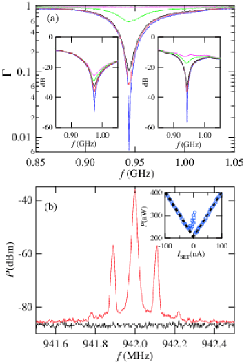
Response of our RF-SSETs to a charge excitation was measured with a spectrum analyzer; typical data are shown in Fig. 3(b). The charge sensitivity is determined from the rms charge excitation amplitude and the signal-to-noise ratio in dB (SNR) of a sideband from where BW is the measurement bandwidth. The best charge sensitivity for sample B is , about three times better than that achieved with a lossy network and the same rf setup.Thalakulam et al. (2004) We calibrated our system noise temperature for sample B by measuring the total noise power versus the dc SET current (Fig. 3(b), inset). At higher bias, the noise varies linearly with due to the SET shot noise.Aassime et al. (2001b) The contribution from the HEMT amplifier is determined by the crossing point of the two fitting curves at . We obtain an amplifier noise power for a measurement bandwidth , giving a noise temperature . The uncoupled energy sensitivity of sample B is , approaching the shot noise limit for the RF-SET.Korotkov and Paalanen (1999); Devoret and Schoelkopf (2000) Without the contribution from the cryogenic amplifier we estimate . For sample A, we measured similar values of and .
Embedding the RF-SSET in the on-chip matching network shows potential for studying the shot noise of the SET for either rf or dc biases by making several improvements in our system. First, the for optimal charge sensitivity in sample B was about (point M in Fig. 2(a)), while near-perfect matching occurred at . Further improvements in the matching network design should allow us to reduce and increase for better matching with higher without lowering the resonant frequency. Also, using a HEMT amplifier with lower noise temperature will improve both the charge and uncoupled energy sensitivity. Finally, improved fabrication techniques for the SET may also lead to a better charge sensitivity.
This work was supported by the NSF under Grant No. DMR-0454914 and by the ARO under Agreement No. W911NF-06-1-0312.
References
- Shor (1994) P. W. Shor, in Proceedings of the 35th Annual Symposium on the Foundations of Computer Science, edited by S. Goldwasser (IEEE Computer Society, Los Alamitos, CA, 1994), pp. 124–134.
- Grover (1997) L. K. Grover, Phys. Rev. Lett. 79, 325 (1997).
- Elzerman et al. (2004) J. M. Elzerman, R. Hanson, L. H. Willems van Beveren, B. Witkamp, L. M. K. Vandersypen, and L. P. Kouwenhoven, Nature 430, 431 (2004).
- Petta et al. (2005) J. R. Petta, A. C. Johnson, J. M. Taylor, E. A. Laird, A. Yacoby, M. D. Lukin, C. M. Marcus, M. P. Hanson, and A. C. Gossard, Science 309, 2180 (2005).
- Knobel and Cleland (2003) R. G. Knobel and A. N. Cleland, Nature 424, 291 (2003).
- LaHaye et al. (2004) M. D. LaHaye, O. Buu, B. Camarota, and K. C. Schwab, Science 304, 74 (2004).
- Braginsky and Khalili (1992) V. B. Braginsky and F. Ya. Khalili, Quantum Measurement (Cambride University Press, Cambridge, 1992).
- Devoret and Schoelkopf (2000) M. H. Devoret and R. J. Schoelkopf, Nature 406, 1039 (2000).
- Schoelkopf et al. (1998) R. J. Schoelkopf, P. Wahlgren, A. A. Kozhevnikov, P. Delsing, and D. E. Prober, Science 280, 1238 (1998).
- Aassime et al. (2001a) A. Aassime, G. Johansson, G. Wendin, R. J. Schoelkopf, and P. Delsing, Phys. Rev. Lett. 86, 3376 (2001a).
- Aassime et al. (2001b) A. Aassime, D. Gunnarsson, K. Bladh, P. Delsing, and R. Schoelkopf, Appl. Phys. Lett. 79, 4031 (2001b).
- Brenning et al. (2006) H. Brenning, S. Kafanov, T. Duty, S. Kubatkin, and P. Delsing, J. Appl. Phys. 100, 114321 (2006).
- Clerk et al. (2002) A. A. Clerk, S. M. Girvin, A. K. Nguyen, and A. D. Stone, Phys. Rev. Lett. 89, 176804 (2002).
- Makhlin et al. (2001) Yu. Makhlin, G. Schön, and A. Shnirman, Rev. Mod. Phys. 73, 357 (2001).
- Abrie (2000) P. L. D. Abrie, Design of RF and Microwave Amplifiers and Oscillators (Artech House, Boston, 2000).
- Stevenson et al. (2002) T. R. Stevenson, F. A. Pellerano, C. M. Stahle, K. Aidala, and R. J. Schoelkopf, Appl. Phys. Lett. 80, 3012 (2002).
- Thalakulam et al. (2004) M. Thalakulam, Z. Ji, and A. J. Rimberg, Phys. Rev. Lett. 93, 066804 (2004).
- Roschier et al. (2004) L. Roschier, P. Hakonen, K. Bladh, P. Delsing, K. W. Lehnert, L. Spietz, and R. J. Schoelkopf, J. Appl. Phys. 95, 1274 (2004).
- Korotkov and Paalanen (1999) A. N. Korotkov and M. A. Paalanen, Appl. Phys. Lett. 74, 4052 (1999).