Near-Field Focusing Plates and Their Design
Abstract
This paper describes the design of near-field focusing plates, which are grating-like structures that can focus electromagnetic radiation to spots or lines of arbitrarily small subwavelength dimension. A general procedure is outlined for designing a near-field plate given a desired image, and its implementation at microwave frequencies is discussed. Full-wave (method of moments) simulations clearly demonstrate the near-field plate’s ability to overcome the diffraction limit. Finally, it is shown that performance of near-field plates is weakly affected by losses.
Index Terms:
near-field, evanescent waves, focusing, lens, metamaterials.I Introduction
The electromagnetic near-field has intrigued scientists and engineers alike since the time Synge first proposed detecting the near-field to obtain resolutions beyond the Abbé diffraction limit [1]. Synge showed that probing the near-field (evanescent waves) of an object amounted to tapping into the object’s subwavelength details. Nearly fifty years after Synge’s proposal, Ash and Nicholls experimentally verified that near-field imaging was possible in 1972 [2]. By scanning the near-field of an object they were able to achieve a resolution at microwave frequencies. Experimental verification at visible wavelengths was subsequently demonstrated in the 1980’s [3, 4].
In addition to detecting the near-field, manipulating and focusing it have attracted significant attention in recent years. Much of this current interest stems from the perfect lens concept introduced by Pendry in 2000 [5]. Pendry showed that a planar slab of negative refractive index material can manipulate the near-field in such a way that it achieves perfect imaging i.e., a perfect reconstruction of the source’s near and far-field. He also showed that the near-field could be focused with only a negative permittivity slab. The experimental verification of negative refraction [6] and subwavelength focusing using negative refractive index [7] and negative permittivity slabs [8, 9], have demonstrated that near-field lenses are in fact a reality.
In [10], an alternative method to manipulate and focus the near-field was proposed, which relies on a patterned (grating-like) planar structure. The proposed planar structure will be referred to as a near-field focusing plate. The near-field plates described in [10] are capable of focusing electromagnetic radiation to spots or lines, of arbitrarily small subwavelength size. These plates can be thought of as impedance sheets that have a modulated surface reactance. The sheets focus the field of a plane wave incident from one side to the other side with subwavelength resolution.
This paper describes the design of near-field focusing plates. It explains how the field at the exit face of such a near-field plate can be derived given a desired image at the near-field plate’s focal plane. In addition, a procedure is outlined for designing a near-field plate to achieve a specific image. Finally, a microwave implementation is discussed. Full-wave (method of moments) results are presented that clearly demonstrate the plate’s ability to overcome the diffraction limit, that is, to focus microwaves to subwavelength dimensions.
II Finding the Fields at the Near-Field Focusing Plate
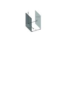
Throughout this paper it will be assumed that the near-field plate is located along the plane and extends in the and directions as shown in Figure 1. Furthermore, it will be assumed that the focal plane of the near-field plate is located at . In order to design a near-field plate, we must first select what image we desire to have at the focal plane. From the image, we can then proceed to derive the fields that must be present at the surface of the near-field focusing plate. First, a Fourier transform is taken of the image to obtain its plane-wave spectrum :
| (1) |
where the harmonic time dependence is . The plane-wave spectrum of the image is then back-propagated to the plane of the near-field plate, located at :
| (2) |
where
| (3) |
and is the wavenumber in free space. Back-propagation refers to the process of reversing the phase of the propagating plane-wave spectrum and growing (restoring) the evanescent plane-wave spectrum, in order to recover the complete plane-wave spectrum at the near-field plate (). Finally, summing the plane-wave spectrum at one recovers the field at the near-field focusing plate:
| (4) |
Given the field at the surface of the near-field focusing plate, one can then proceed to design the plate itself. The design process involves finding a surface impedance that yields the desired field at the near-field focusing plate.
III A Near-field Focusing Plate in Two Dimensions
As discussed in [10], various near-field plates can be envisioned that produce focal patterns of various types and symmetries. Although the design procedure outlined in this paper is quite general, we will consider a simple near-field plate that focuses evanescent waves in two dimensions ( and ). The coordinate will denote the direction transverse to the near-field focusing plate and the direction normal to the surface of the plate (see Figure 1). For this particular design, the image along the focal plane () is chosen to be a sinc function of the following form:
| (5) |
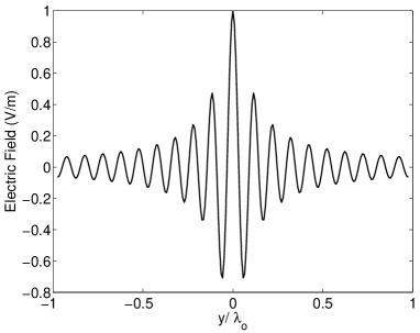
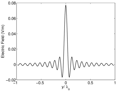
where and , is the wavenumber in free space. The image given by Equation (5) has a flat evanescent-wave spectrum of magnitude that extends between , as depicted in Figure 2.
Such an image could be expected when imaging a line source with a negative permittivity slab (a silver superlens) [5, 8, 9]. The propagating spectrum is zero at the focal plane since it is totally reflected by the negative permittivity slab, but the evanescent spectrum is still present. The spatial frequency represents a cut-off wavenumber, above which transmission through the slab rapidly falls off. However, instead of having the evanescent spectrum fall off as in focusing using a negative permittivity slab, we have simply assumed that it is truncated beyond . This cut-off wavenumber is dictated by the inherent losses of the negative permittivity slab [11, 12]. Under the condition that the image simplifies to:
| (6) |
To find what field distribution is needed at the near-field plate to produce such an image, we back-propagate the plane-wave spectrum of the image and then sum it up at :
| (7) |
Since we are in the subwavelength region () . Therefore, Equation (7) can be expressed as,
| (8) |
Performing the above integration, the following expression is obtained for the field at the surface of the near-field plate:
| (9) |
Given that , this expression simplifies to:
| (10) |
From Equations (6) and (10), it is apparent that the field at the near-field plate decays toward the focal plane. Specifically, the amplitude of the field along decays from the near-field plate () to the focal plane () by an amount equal to:
| (11) |
The fields and , given by Equations (10) and (6) respectively, are plotted in Figure 3 for the case where and .
From Equation (6), it can also be found that the null-to-null beamwidth of the image at the focal plane () is:
| (12) |
Expressing as a multiple of the free-space wavenumber , the null-to-null beamwidth of the image can be rewritten as:
| (13) |
where is the wavelength in free space, and is what has often been referred to as the resolution enhancement [11, 13]. Further, expressing the distance to the focal plane as a fraction of a free-space wavelength , the decay of the field (Equation (11)) along the axis from the near-field plate to the focal plane can be rewritten as:
| (14) |
From Equation (14) it can be concluded that the ratio of cannot be excessively high for the signal to still be detectable at the focal plane of the near-field plate.
IV Designing a Near-Field Focusing Plate
Equation (10) indicates that the field at the near-field plate exhibits both phase and amplitude variation. A simple way to generate such a field distribution is to illuminate a reactance sheet located at from the direction with a plane wave. The sheet should have a surface reactance that is a function of position corresponding to the phase and amplitude variation of the field.
To see how such a reactance sheet (near-field plate) can be designed, let us first consider the simplified problem of transmission through a sheet with uniform surface impedance. For normal incidence, the transmission coefficient through a uniform sheet is:
| (15) |
where is the impedance of free-space, and is the surface impedance of the reactance sheet. If the surface impedance of the sheet is low (), the transmission coefficient through the sheet can be approximated as:
| (16) |
For this special case, the transmitted field is low, but its magnitude and phase ( or ) can be accurately controlled. For example, if the reactance of the sheet is inductive (of the form ), the transmission coefficient through the sheet has a phase of , while if it is capacitive (of the form ) the phase is . As a result, capacitive and inductive surface impedances can be used to produce fields that are out of phase. One can also change the magnitude of the transmitted field by varying the magnitude of the inductive or capacitive sheet reactance. Therefore, by using a sheet with a reactance that is modulated as a function of , one can synthesize various field profiles including the one given in Equation (10).
From the above discussion, it is clear that the reactance of an impedance sheet can be manipulated to control the transmitted electromagnetic field. Now let us consider the design of a near-field plate (a specific type of impedance sheet) that focuses energy from a plane wave to subwavelength dimensions at the plane. The plane wave is assumed to be polarized along the direction and normally incident from the direction onto the near-field plate located at . The dependent surface impedance of the near-field plate will be represented as . Similarly, the -directed current density induced on the near-field plate will be represented as . The boundary condition along the reactance sheet (near-field plate) can then be represented as a Fredholm integral equation of the second kind:
| (17) |
where is the amplitude of the incident plane wave at , is a Hankel function of the second kind of order zero, and is the width of the near-field plate. In the integral equation the unknown current density appears both inside and outside of the integral sign. The total field at the surface of the near-field plate therefore is:
| (18) |
Equating to the field desired at the surface of the near-field plate, given by Equation (10), one can solve for . Equation (10) has been multiplied by the scaling factor to obtain the following equation for :
| (19) |
The desired field has been multiplied by the imaginary number in order to obtain predominantly passive (inductive and capacitive) surface impedances for the near-field plate design. The variable represents the amplitude of as a multiple of the incident field . A larger represents a higher field amplitude at the surface of the near-field plate (), and therefore a more highly resonant plate. To obtain the unknown current density , Equation (18) can be solved numerically using the method of moments. Finally, dividing by the computed current distribution , the surface impedance can be found. Once the surface impedance is found the design of the near-field plate is complete.
The procedure for deriving does not ensure that is passive. To enforce that the lens is entirely passive, only the imaginary part of the derived is taken. The current density is then solved for again by plugging the passive into Equation (17). Once the current density is found for the passive near-field plate, the fields scattered by the near-field plate are computed using the two dimensional free-space Green’s function:
| (20) |
The total field at any point is then the sum of the incident plane-wave and the scattered field due to the induced current density on the near-field plates.
Now let us consider a specific near-field plate design at 1.0 GHz (). For this particular design , or equivalently . In addition, the focal plane is chosen to be from the near-field plate. Hence, the near-field plate is capable of creating a focal spot with a null-to-null beamwidth of at a distance from the plate. In addition, the width of the near-field plate () is chosen to be approximately wavelengths in the direction and the constant is set to . In other words, the field at is six times the amplitude of the incident plane wave ().
The current density on the near-field plate is discretized into 79 segments in order to solve Equation (19) numerically. The segments are centered at positions , where is an integer from -39 to 39, and is the width of each segment. The variable is chosen to be to mimic a continuous variation in surface impedance: . Collocation (the point matching method) [14] was used to solve for the current density on the near-field plate, from which the surface impedance of the near-field plate was subsequently found. In the computations it was assumed that the incident plane wave is equal to at the surface of the near-field plate. Table I shows the surface impedances of the segments comprising the near-field plate. Since the plate is symmetric, the surface impedances of only 40 segments ( to ) are shown. Column two of Table 1 shows the impedances that are derived directly from Equation (19), while those in column 3 are the passive surface impedances used in the design of the passive near-field plate. They are completely imaginary and thus represent inductive and capacitive surface impedances.
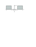
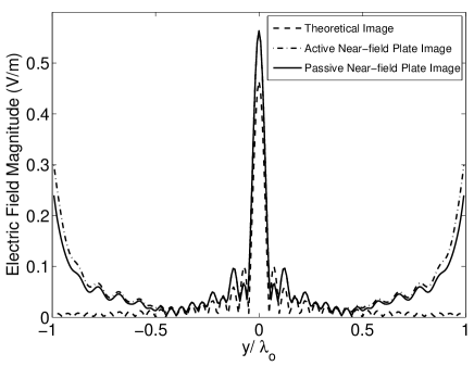
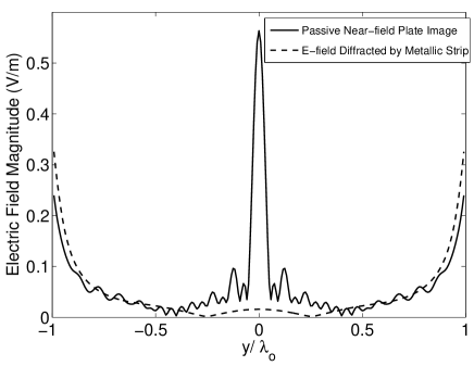
Plotted in Figure 4 are different electric field profiles at the focal plane. The dotted line shows the theoretically predicted image, which is simply a plot of Equation (6) multiplied by the constant . The dash-dot line represents the image that would be produced by the near-field plate possessing the surface impedances given in column 2 of Table I. This active near-field lens possesses reactances as well as positive (loss) and negative (gain) resistive elements. Finally, the solid line represents the image formed by the passive near-field focusing plate. The active and passive plate images have a mainlobe that is . The difference between the two images is minimal, and they are both quite close to the theoretically predicted image (dotted line). The images of the active and passive plates, however, possess an increase in field magnitude near . This rise in field magnitude is due to the diffraction of the incident plane wave from the edges of the near-field focusing plate. Figure 5 compares the electric field diffracted by a metallic strip that is two wavelengths wide to the electric field diffracted by the near-field plate of the same width. As can be seen from the plot, the electric field diffracted by the metallic strip follows the field diffracted by the near-field focusing plate near . This plot supports the fact that the rise in electric field magnitude in Figure 5 is due to diffraction. On the other hand, the electric field around is quite different since the near-field focusing plate manipulates the evanescent spectrum to create a sharp image, while the metallic strip does not.
V Loss Performance
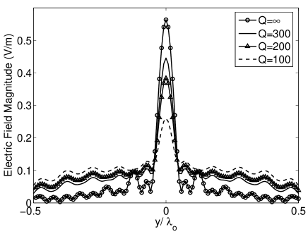
Near-field focusing is a resonant phenomenon which degrades with increased losses. In order to study the performance of a practical near-field focusing plate, loss was added to the purely reactive surface impedances of the passive plate given in column 3 of Table 1. The loss associated with a reactance is typically expressed in terms of the quality factor, , which is defined as the ratio of the surface reactance (imaginary surface impedance) to the surface resistance (real surface impedance):
| (21) |
Figure 6 shows the focus for near-field plates with various quality factors. For each graph, all surface impedances were assigned the same quality factor. The plots show that the central peak of the focus decreases and the sidelobes increase with increasing loss. However, it is encouraging that the degradation of the focus is gradual. For a printed metallic near-field focusing plate at frequencies of a few gigahertz, quality factors of a couple hundred can be expected. For such values of Q, the near-field focusing is still very prominent. In practice, the inductive surface impedances could be implemented as inductively loaded metallic strips/wires while the capacitive surface impedances could be implemented as capacitively loaded strips or metallic patches printed on a microwave substrate. At optical frequencies, the inductive surface impedances could be implemented using nanofabricated plasmonic structures and the capacitive surface impedances using dielectric structures [15].
VI Conclusion
The intrinsic properties and design of near-field focusing plates have been described. These plates are planar structures that have the ability to focus electromagnetic waves to subwavelength dimensions. Moreover, a procedure has been outlined for designing a near-field plate to achieve a desired image. Full-wave simulations at microwave frequencies, have clearly demonstrated the near-field plate’s ability to overcome the diffraction limit. The effect of losses on the performance of near-field focusing plates has also been addressed. At microwave frequencies, near-field focusing plates may find use in non-contact sensing and microwave imaging applications. At optical frequencies, applications of this technology may include lithography, microscopy and near-field optical data storage.
| Passive | ||
|---|---|---|
| 0 | -0.0540 -24.8811i | -24.8811i |
| 1 | -0.3078 -34.9762i | -34.9762i |
| 2 | 0.0497 -18.8400i | -18.8400i |
| 3 | 0.0830 -22.1429i | -22.1429i |
| 4 | -0.0866 -17.4066i | -17.4066i |
| 5 | -0.0874 -21.3768i | -21.3768i |
| 6 | 0.0968 -14.1181i | -14.1181i |
| 7 | 0.0705 -18.3300i | -18.3300i |
| 8 | -0.2215 -18.0665i | -18.0665i |
| 9 | -0.0862 -20.3643i | -20.3643i |
| 10 | 0.1165 -12.1702i | -12.1702i |
| 11 | 0.0536 -17.3865i | -17.3865i |
| 12 | -0.3545 -22.2030i | -22.2030i |
| 13 | -0.0480 -20.5220i | -20.5220i |
| 14 | 0.0419 -10.3653i | -10.3653i |
| 15 | 0.0049 -16.8255i | -16.8255i |
| 16 | 0.3176 -33.9907i | -33.9907i |
| 17 | 0.0482 -20.9474i | -20.9474i |
| 18 | -0.0994 - 8.6930i | - 8.6930i |
| 19 | -0.0696 -16.3809i | -16.3809i |
| 20 | 27.6488 -97.2412i | -97.2412i |
| 21 | 0.1922 -21.4451i | -21.4451i |
| 22 | -0.2328 - 7.2934i | - 7.2934i |
| 23 | -0.1455 -16.0315i | -16.0315i |
| 24 | 29.1460 +63.0469i | +63.0469i |
| 25 | 0.3231 -21.8837i | -21.8837i |
| 26 | -0.2867 - 6.2742i | - 6.2742i |
| 27 | -0.1752 -15.7837i | -15.7837i |
| 28 | 5.6876 +26.9105i | +26.9105i |
| 29 | 0.2934 -22.2145i | -22.2145i |
| 30 | -0.1685 - 5.5034i | - 5.5034i |
| 31 | -0.0641 -15.6296i | -15.6296i |
| 32 | -0.1209 +17.9582i | +17.9582i |
| 33 | -0.2211 -22.4108i | -22.4108i |
| 34 | 0.3371 - 4.9484i | - 4.9484i |
| 35 | 0.4372 -15.5174i | -15.5174i |
| 36 | -5.3426 + 9.7995i | + 9.7995i |
| 37 | -2.4484 -22.4780i | -22.4780i |
| 38 | 1.7231 - 3.3621i | - 3.3621i |
| 39 | 4.4763 -13.2700i | -13.2700i |
References
- [1] E. H. Synge, “A Suggested Method For Extending the Microscopic Resolution into the Ultramicroscopic Region,” Phil. Mag., vol. 6, pp. 356–362, 1928.
- [2] E.A. Ash and G. Nicholls, “Super-Resolution Aperture Scanning Microscope,” Nature, vol. 237, pp. 510–512, June 1972.
- [3] D.W. Pohl, W. Denk , and M. Lanz, “Optical Stethoscopy: Image Recording With Resolution ,” Applied Physics Letters, vol. 44, pp. 651–653, April 1984.
- [4] A. Lewis, M. Isaacson, A. Harootunian, and A. Murray, “Development of a 500- Spatial-Resolution Light-Microscope,” Ultramicroscopy, vol. 13, pp. 227–231, 1984.
- [5] J.B. Pendry, “Negative Refraction Makes a Perfect Lens,” Physical Review Letters, vol. 85, pp. 3966–3969, October 2000.
- [6] R.A. Shelby, D.R. Smith, and S. Schultz, “Experimental Verification of a Negative Index of Refraction,” Science, vol. 292, pp. 77–79, April 2001.
- [7] A. Grbic and G.V. Eleftheriades, “Overcoming the Diffraction Limit With a Planar Left-Handed Transmission-Line Lens,” Physical Review Letters, vol. 92, p. 117403, March 2004.
- [8] N. Fang, H. Lee, C. Sun, and X. Zhang, “Sub-Diffraction-Limited Optical Imaging With a Silver Superlens,” Science, vol. 308, pp. 534–537, April 2005.
- [9] D. Melville and R. Blaikie, “Super-Resolution Imaging Through a Planar Silver Layer,” Optics Express, vol. 13, pp. 2127–2134, March 2005.
- [10] R. Merlin, “Radiationless Electromagnetic Interference: Evanescent-Field Lenses and Perfect Focusing,” Science Express, vol. 10.1126/science.1143884, July 12 2007.
- [11] D.R. Smith, D. Schurig, R. Rosenbluth, S. Schultz, S.A. Ramakrishna, and J.B. Pendry, “Limitations on Subdiffraction Imaging with a Negative Refractive Index Slab,” Applied Physics Letters, vol. 82, pp. 1506–108, March 2003.
- [12] R. Merlin, “Analytical Solution of the Almost-Perfect-Lens Problem,” Applied Physics Letters, vol. 84, pp. 1290–1292, February 2004.
- [13] A. Grbic and G.V. Eleftheriades, “Practical Limitations of Subwavelength Resolution Using Negative-Refractive-Index Transmission-Line Lenses,” IEEE Transactions on Antennas and Propagation, vol. 53, pp. 3201–3209, October 2005.
- [14] R. F. Harrington, Field Computation by Moment Methods. Wiley-IEEE Press, 1993.
- [15] N. Engheta, A. Salandrino, and A. Alu, “Circuit Elements at Optical Frequencies: Nanoinductors, Nanocapacitors, and Nanoresistors,” Physical Review Letters, vol. 95, p. 095504, August 2005.