Determination of the Superconductor-Insulator Phase Diagram for One-Dimensional Wires
Abstract
We establish the superconductor-insulator phase diagram for quasi-one-dimensional wires by measuring a large set of MoGe nanowires. This diagram is consistent with the Chakravarty-Schmid-Bulgadaev phase boundary, namely with the critical resistance being equal to . We find that transport properties of insulating nanowires exhibit a weak Coulomb blockade behavior.
pacs:
74.78.Na, 74.25.Dw, 74.40.+kIn quasi-one-dimensional superconductors it remains to be fully understood how the superconducting properties of a wire are destroyed as its diameter is reduced. Years ago it was shown that for wires with micron size diameters the mechanism that weakens superconductivity at finite temperature, , are thermally activated phase slips (TAPS), which break the superconducting phase coherence along the wire and result in a measurable resistance, LAMHetal ; TinkhamBook . As temperature is reduced the thermal fluctuations that cause TAPS freeze out and the TAPS rate decreases faster than exponentially until at these phase slips are absent from the wire altogether and it should be in a truly superconducting state (). However, in the ultrathin wires being fabricated today this simple picture is complicated by an additional phase breaking process due to quantum fluctuations Mooij ; Giordano ; GZQPS . As these quantum phase slips (QPS) remain active and the resistance of a wire remains finite, even at . Since the free energy barrier to phase slips is proportional to the wire’s cross sectional area, the thinner a wire is made the more readily phase slips should occur in it and therefore the QPS resistance is higher Lau ; Arutyunov ; Altomare .
While it would seem that ultrathin superconducting wires loose the beneficial property of dissipationless electrical transport, the remarkable possibility exists to recover the truly superconducting state if QPS are suppressed. Recent experiments on a group of six wires with similar lengths 100 nm observed that as those wires whose normal state resistance, , was less than some critical resistance, , were superconducting, while wires with were resistive, with increasing resistance as Bezryadin . It was found that , where , which is suggestive of a Chakravarty-Schmid-Bulgadaev (CSB) dissipative phase transition CSB , in which QPS can be inhibited due to the interaction with a dissipative environment. This transition was originally predicted for shunted Josephson junctions but recently theoretically generalized for thin wires Buchler ; RefaelJJ ; RefaelRT ; RefaelNew . Unfortunately, these early experiments could not provide a proof of the universality of the condition . Furthermore, it is not clear whether a real superconductor-insulator transition (SIT) occurs in ultrathin superconducting wires or merely a crossover from wires in which the QPS rate is too small to be of consequence and so appear superconducting to wires in which the QPS rate is so large they essentially drive the wire into the normal state. Distinguishing between these two possibilities is of critical importance not only to our understanding of the physics of quasi-one-dimensional superconducting wires but also to their applicability in miniaturized superconducting circuits TinkhamAPL .
In this Letter, we present results obtained on a large collection of about 100 wires that provide definitive evidence for the SIT and show that for short wires the phase boundary is the same as in the CSB transition, suggesting the same physical mechanism. No indication of a crossover caused by a gradual increase of the QPS rate was found. The wires have been characterized by linear transport measurements as well as high-bias differential resistance measurements. The results allow us to sort most of the homogeneous samples into two categories, “superconducting” and “insulating”, and to construct a phase diagram with a well defined boundary for the SIT in thin wires. This diagram will provide an experimental basis for the theory of thin superconducting wires, which is still being developed GZQPS ; Buchler ; RefaelRT ; RefaelNew ; Sachdev ; Khlebnikov .
The nanowires used in this study were fabricated by molecular templating Bezryadin , by depositing amorphous Graybeal Mo0.79Ge0.21 (sputtered MoGe thicknesses were in the range 4-16 nm) onto insulating fluorinated single-wall carbon nanotubes that were suspended over a trench etched into Si/SiO2/SiN substrates. The wires were carefully examined by scanning electron microscopy (SEM) and the choice of the wire for transport measurements was influenced by such factors as apparent homogeneity, straightness of the wire, desired dimensions, and good connection of the wire to the films on either side of the trench (SEM measured lengths and widths of the wires were in the ranges 29-490 nm and 8.8-40.0 nm, respectively). Transport measurements were performed in 4He and 3He cryostats, and some samples were further tested in a top-loading dilution refrigerator. Each system had and microwave filtering placed at room- and low-temperature stages, respectively.
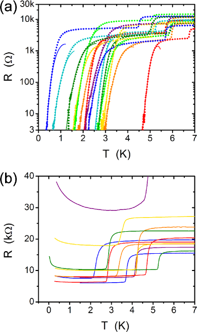
The phase to which a nanowire belongs is easily discerned by the transport properties of the wire. In Fig. 1 we show the curves for some representative samples. Note that upon cooling all samples initially show a superconducting transition at the critical temperature of the thin film electrodes, , that are measured in series with the wire. For the resistance of the electrodes is zero and we probe only the wire. The normal state resistance of a wire, , is assumed to be the sample resistance just below .
Superconducting wires (Fig. 1(a)) show resistive transitions that are well described by the TAPS theory (details of the fitting procedure can be found in Ref. RogachevPRL1 ; alternate methods are given in Refs. RefaelRT ; KhlebnikovRT ). We emphasize that for wires in the superconducting phase no resistance “tails” or other non-TAPS behavior that could possibly be attributed to QPS are observed, even for those wires near the SIT. However, one should be careful in interpreting this result. According to the microscopic theory of Zaikin et al. GZQPS , the contribution to resistance from QPS, where is the zero-temperature coherence length and is the length of the wire, contains a numerical factor, , that is of order one and depends on the actual dependence of the order parameter phase on time and space coordinates during the QPS process. We find that setting this coefficient to is enough to suppress the expected contribution from QPS below the level of noise in the experiments, and so free QPS, if they do indeed occur in the superconducting wires, can not be resolved. While this value for is different from the value of found in Ref. Markovic , it is still of order one as required by the theory. But this is not the end of the story since one also needs to test the same expression with the same “a” on the insulating wires.
The curves of wires in the insulating phase (Fig. 1(b)), with resistance that increases upon cooling, are clearly different from those in the superconducting phase. One way to understand the insulating regime would be to consider it qualitatively the same as the superconducting regime, except that the QPS rate is higher due to the smaller diameter of the wires. In such a crossover model, the QPS occur in all wires, all wires retain some non-zero resistance at zero temperature, and the QPS parameter is the same for all wires. However, this model does not explain the abruptness of the transition observed: The wires are either in agreement with the TAPS model or show an insulating behavior. We did not observe any intermediate regime with a mixture of TAPS and QPS contributions even though a large set of wires was studied. Reentrant behavior, i.e. resistance increasing with cooling and then suddenly dropping, was never observed as well. Also, such a crossover model quantitatively contradicts the value discussed above. The predicted resistance from QPS at with for some of the typical insulating wires is less than 1% of (and frequently many orders of magnitude less than this), which is never observed (the observed value is always slightly greater than (Fig. 1(b))). We found that there is no single value of the coefficient that can explain the whole set of data. Thus, we suggest that the correct model for quasi-one-dimensional superconducting nanowires should involve an SIT, with the insulating phase characterized by complete elimination of the superconducting condensate, due to proliferating QPS.
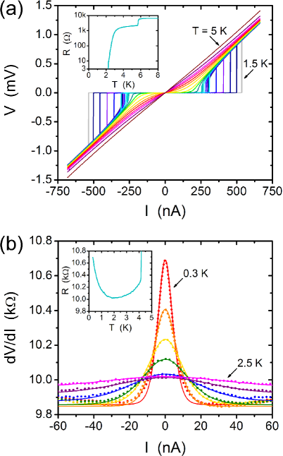
Another dichotomy in transport properties is also found in the voltage vs. current, , characteristics of the wires. In Fig. 2(a), curves for a representative superconducting sample at different temperatures show the evolution of the behavior of wires in this phase from linear for , to nonlinear for , to hysteretic for with well defined switching and retrapping currents. Insulating wires, on the other hand, display characteristics that are nearly linear at all temperatures but with a zero-bias anomaly that is more pronounced in the differential resistance, , measurements. For a representative insulating sample we show data at different temperatures in Fig. 2(b). Since a small zero-bias maximum can be observed even for those temperatures at which is at its minimum, the peak cannot be a result of Joule heating. Instead, as shown by the fits in Fig. 2(b), the zero-bias anomaly can be described by the theory of dynamical weak Coulomb blockade with the entire wire acting as a coherent scatterer, the same as for the curves for these wires BollingerEPL ; NGZCS .
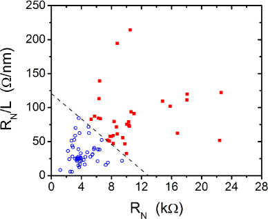
We now turn our attention to the main result of this Letter - the phase diagram of the SIT in quasi-one-dimensional nanowires. Based upon the transport measurements the wires fall into one of two distinct phases: superconducting or insulating EndNote1 . In Fig. 3 we plot the phase to which a wire belongs on the coordinate plane (,). If the SIT in ultrathin wires is caused by local physics then there should exist a critical cross sectional area, , that separates insulating and superconducting wires. For the range of MoGe thicknesses sputtered, the resistivity does not change with thickness Graybeal and so the separatrix in this scenario should appear on Fig. 3 as a horizontal line with . This is certainly not the phase boundary we observe. Rather, the CSB phase boundary, i.e. (dashed line in Fig. 3) provides a much better division of the data. It is observed that three longer wires (450 nm) behave as superconductors even though they have high normal resistance, i.e. . These deviations suggest that the SIT is only applicable to shorter wires, as predicted in Ref. RefaelNew, .
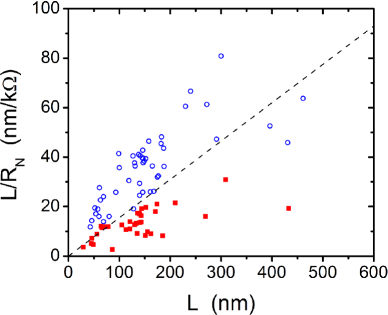
Some short wires with somewhat lower than appear insulating. These deviations can be explained by assuming that our knowledge about the effective is not precisely correct. The effective might in fact go above the measured as the temperature is reduced. A proximity effect can also be responsible for the imprecise knowledge of the effective of the wire. However, these deviations may point to other phenomena occurring in these wires. In Fig. 4 we plot the state of wires on the (,) coordinate plane. In this representation it is clear that a single line can be drawn that separates precisely the superconducting and insulating phase. The phase boundary is given by nm. Samples below the line are superconducting while those above it are insulating. A more useful form of this boundary is obtained by using , where is the cross sectional area of the wire, and the typical value for the normal metal resistivity of MoGe, 180 -cm Graybeal . Thus the separatrix simply is where nm. The superconducting (insulating) phase occurs for samples with (). This means that for wires that have the superconductivity is lost if the wire diameter, , is less than the critical diameter nm. This critical diameter is quantitatively consistent with our recent conjecture that superconductivity in ultrathin wires is affected, in accordance with the Abrikosov and Gor’kov mechanism, by magnetic moments that spontaneously form on the wire surface RogachevPRL2 . Assuming that magnetic pair breaking is responsible for the destruction of superconductivity in MoGe wires with one can estimate the critical diameter from the empirical law relating wire diameter to the exchange scattering time, , found in Ref. RogachevPRL2 . The critical exchange scattering time, below which is zero, is given by where , is the critical depairing factor, is Euler’s constant, and is the critical temperature of the wire in the absence of pair breaking effects. In Ref. RogachevPRL2 , a fit to vs. data for MoGe nanowires showed that nm/ps and was found to be in the range K. This corresponds to ps and nm, in agreement with the value of obtained from Fig. 4. Finally, we point out that the empirical phase boundary in Fig. 4 suggests that wires with will become insulating if , i.e. when localization effects become strong.
In conclusion, we have studied a large set of nanowire samples with lengths and normal state resistances in the ranges of 29-490 nm and 1.17-32.46 k, respectively. The phase diagram of the SIT is in good, albeit not exact, agreement with the one expected for the CSB transition, in accordance with the theory of Ref. RefaelNew, . The few deviations can be accounted for by the destruction of superconductivity due to local magnetic moments in wires that would otherwise belong to the superconducting part of the diagram. This comparison with the CSB phase boundary assumes that can be considered as an effective shunting resistance as validated by Ref. RefaelNew, .
Acknowledgements.
We thank M.W. Brenner, E. Demler, G. Refael, M. Sahu, and T.-C. Wei for assistance and discussions. The work was supported by the U.S. Department of Energy, Division of Materials Sciences under Award No. DEFG02-91ER45439, through the Frederick Seitz Materials Research Laboratory at the University of Illinois at Urbana-Champaign and the NSF CAREER Grant DMR 01-34770.References
- (1) Present address: Condensed Matter Physics and Materials Science Department, Brookhaven National Laboratory, Upton, NY 11973, USA.
- (2) Present address: Department of Physics, University of Utah, Salt Lake City, UT 84112, USA.
- (3) W.A. Little, Phys. Rev. 156, 398 (1967); J.S. Langer and V. Ambegaokar, ibid. 164, 498 (1967); D.E. McCumber and B.I. Halperin, Phys. Rev. B 1, 1054, (1970); R.S. Newbower, M.R. Beasley, and M. Tinkham, ibid. 5, 864 (1972); J.E. Lukens, R.J. Warburton, and W.W. Webb, Phys. Rev. Lett. 25, 1180 (1970).
- (4) M. Tinkham, Introduction to Superconductivity (McGraw Hill, New York, 1996).
- (5) A.J. van Run, J. Romijn, and J.E. Mooij, Jpn J. Appl. Phys. 26, Suppl. 26-3-2, 1765 (1987).
- (6) N. Giordano, Phys. Rev. Lett. 61, 2137 (1988); N. Giordano and E.R. Schuler, Phys. Rev. Lett. 63, 2417 (1989).
- (7) A.D. Zaikin et al., Phys. Rev. Lett. 78, 1552 (1997); D.S. Golubev and A.D. Zaikin, Phys. Rev. B 64, 014504 (2001).
- (8) C.N. Lau et al., Phys. Rev. Lett. 87, 217003 (2001).
- (9) M. Zgirski et al., Nano Lett. 5, 1029 (2005).
- (10) F. Altomare et al., Phys. Rev. Lett. 97, 017001 (2006).
- (11) A. Bezryadin, C.N. Lau, and M. Tinkham, Nature 404, 971 (1999).
- (12) S. Chakravarty, Phys. Rev. Lett. 49, 681 (1982); A. Schmid, ibid. 51, 1506 (1983); S.A. Bulgadaev, JETP Lett. 39, 315 (1984).
- (13) H.P. Büchler, V.B. Geshkenbein, and G. Blatter, Phys. Rev. Lett. 92, 067007 (2004).
- (14) G. Refael et al., Phys. Rev. B 68, 214515 (2003); 75, 014522 (2007).
- (15) D. Meidan, Y. Oreg, and G. Refael, Phys. Rev. Lett. 98, 187001 (2007).
- (16) G. Refael, E. Demler, and Y. Oreg, arXiv.org:0803.2515 (2008).
- (17) M. Tinkham and C.N. Lau, Appl. Phys. Lett. 80, 2946 (2002).
- (18) S. Sachdev, P. Werner, and M. Troyer, Phys. Rev. Lett. 92, 237003 (2004).
- (19) S. Khlebnikov, Phys. Rev. Lett. 93, 090403 (2004); S. Khlebnikov and L.P. Pryadko, ibid. 95, 107007 (2005).
- (20) J.M. Graybeal and M.R. Beasley, Phys. Rev. B 29, 4167 (1984); J.M. Graybeal, Ph. D. Thesis, Stanford University, 1985.
- (21) A. Rogachev, A.T. Bollinger, and A. Bezryadin, Phys. Rev. Lett. 94, 017004 (2005).
- (22) S. Khlebnikov, Phys. Rev. B 77, 014505 (2008).
- (23) N. Marković, C.N. Lau, and M. Tinkham, Physica C 387, 44 (2003).
- (24) A.T. Bollinger, A. Rogachev, and A. Bezryadin, Europhys. Lett. 76, 505 (2006).
- (25) Y.V. Nazarov, Phys. Rev. Lett. 82, 1245 (1999); D.S. Golubev and A.D. Zaikin, ibid. 86, 4887 (2001).
- (26) As was demonstrated in Ref. BollingerPRB , inhomogeneous samples usually can not be characterised decisively as superconducting or insulating. Thus we did not include such samples on the SIT diagram. Also, among the samples that did not show clear signs of inhomogeneity, two samples showed a behavior intermediate between superconducting and insulating. We explain this by probable hidden inhomogeneity as an atypical time lag occured between fabrication and measurement for these two samples. We also exclude them from the diagram.
- (27) A. Rogachev et al., Phys. Rev. Lett. 97, 137001 (2006).
- (28) A.T. Bollinger et al., Phys. Rev. B 69, 180503(R) (2004).