Spin separation in a T ballistic nanojunction due to lateral-confinement-induced spin-orbit-coupling
Abstract
We propose a new scheme of spin filtering employing ballistic nanostructures in two dimensional electron gases (2DEGs). The proposal is essentially based on the spin-orbit (SO) interaction arising from the lateral confining electric field. This sets the basic difference with other works employing ballistic crosses and T junctions with the conventional SO term arising from 2DEG confinement. We discuss the consequences of this different approach on magnetotransport properties of the device, showing that the filter can in principle be used not only to generate a spin polarized current but also to perform an electric measurement of the spin polarization of a charge current. We focus on single-channel transport and investigate numerically the spin polarization of the current.
pacs:
72.25.-b, 72.20.My, 73.50.JtIntroduction - In recent years a great effort has been devoted to the study and the realization of electric field controlled spin based devicesspintro . Many basic building blocks are today investigated theoretically and experimentally in order to realize a fully spin based circuitry. Among them, a particular relevance is covered by: (i) pure spin current generation, (ii) voltage control of the spin polarization of a current and (iii) the electric detection of this polarization. For the same purpose many works have been focusing on the so called spin Hall effect [3] ; [7] ; Hir ; she2 ; she3 ; she4 and most of the implementations in 2DEGs proposed for the spin manipulation are mainly based on the spin-orbit (SO) interaction. The SO Hamiltonian reads Thankappan
| (1) |
Here is the electric field, are the Pauli matrices, is the canonical momentum operator is a 3D position vector , and the electron mass in vacuum. In materials and are substituted by their effective values and . A significant SO term arises from the interaction of the traveling charge carrier with strong electric fields in solids. The SO term can be seen as the interaction of the electron spin with the magnetic field, , appearing in the rest frame of the electron.
Rashba Coupling - In the case of quantum heterostructures of narrow gap semiconductors, a major contribution to the SO coupling may originate intrinsically from its confining potentialBR . The spin Hall effect in two-dimensional electron systems exploits the Rashba SO coupling (-coupling) due to an asymmetry in quantum well potential that confines the electron gas Kelly . The main component of the SO coupling will be along and the Hamiltonian in Eq. 1 will take the formbonew . in vacuum is while the highest value of in 2DEGs is close to to eV m as reported in refs.[shapers, ; Schultz, ].
The -SO coupling may generate a spin-dependent transverse force on moving electrons1519 ; 1519a ; 1519b ; 1519c . This force tends to separate different spins in the transverse direction as a response to the longitudinal charge current, giving a qualitative explanation for the Rashba spin Hall effect. In the presence of Rashba SO coupling, however, the electron spin, particularly its out-of-plane projection, is not conserved and, hence, the usual continuity equation fails to describe the spin transport. This makes the spin transport phenomena in this system rather complicated.
Lateral-confinement-induced Coupling - Next we consider low dimensional electron systems formed by crossing Quantum Wires (QWs) through the analysis of the SO coupling in a 2D electron system with an in-plane potential gradient. In such systems a confining (-coupling) SO term arises from the in-plane electric potential that is applied to squeeze the 2DEG into a quasi-one-dimensional channel Thornton ; Kelly .
We adapt the general form of eq.(1) to the strictly 2D case, where the degree of freedom of motion in the z direction is frozen out (), and the potential energy, , depends only on and coordinates. Then the SO Hamiltonian in this case can be written in the formmorozb :
| (2) |
The reduced Hamiltonian commutes with the spin operator , and, hence, conserves spin. Thus a SO coupling of this kind generates a spin-dependent force on moving electrons while conserving their spins. The standard continuity equation for spin density and spin current is naturally established because of spin conservation.
The spin-conserving -SO interactions are also at the basis of the quantum spin Hall effects discovered recentlynoish ; qse ; iii ; hatt ; noiq .
Spin Filters - In this paper we investigate the spin polarization of the current in the presence of (spin conserving) -interaction in a T-shaped conductor, in particular we show why a -coupling scheme results in a different working principle, as compared to equivalent structures exploiting -coupling kk .
In fact ”spin filters” based on the -coupling rely on the precession of electrons spins during their motion through the wave guides, while the scheme we propose here, based on the -coupling, preserves the component of the spin at the injection and sends electrons/holes to different stubs according to their spin value. Differently from -coupling schemes the device we propose should in principle allow one, for a given charge current, to electrically measure the spin polarization grade with its sign. As a first step to defend this statement we write down the Hamiltonian of a T-stub with SO -coupling and make some qualitative considerations. In the following step we extract a quantitative analysis of device’s transport properties using materials parameters from the literature.
-SO coupling and effective magnetic field - Here we focus on the case of pure -coupling.
The basic building blocks of the nanojunctions that we discuss in the following are the QWs. The ballistic one-dimensional wire is a nanometric solid-state device in which the transverse motion (along ) is quantized into discrete modes, and the longitudinal motion ( direction) is free. In this case electrons are envisioned to propagate freely down a clean narrow pipe and electronic transport with no scattering can occur.
In a Q1D wire, where a parabolic lateral confining potential3840 along ( for leads and for leads and ) with force is considered () it follows
| (3) |
where is the typical spatial scale and is the other direction in the 2DEG (). Thus, as we discussed in a previous papernoish , in a QW a uniform effective magnetic field, is present along ,
| (4) |
Then an electron of spin flowing in the QW perceives in its rest frame a magnetic field , directed upward or downward according to the sign of . This results in an interesting behavior of junctions between two wires, such as T stubs and cross junctions, when a large enough -coupling is considered.
The discussion reported above for a QW can be generalized to any device patterned in a 2DEG. The Hamiltonian of an electron moving in a 2D device defined by a general confining potential in which the -SO term is negligible can be written as
| (5) | |||||
where and .
The commutation relation,
is equivalent to that of a charged particle in a transverse magnetic field, but here the sign of depends on the direction of the spin along . It follows that electrons with opposite spin states are deflected into opposite terminals by a spin-dependent Lorentz force:
| (6) |
where is a spin dependent inhomogeneous magnetic field, with .
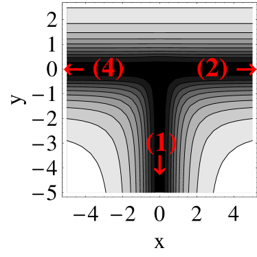
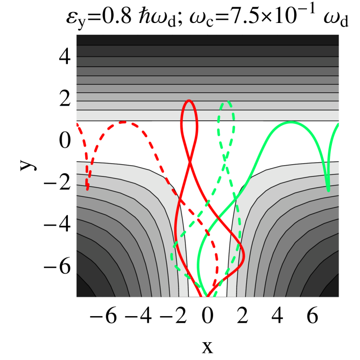
The T junction -In a cross junction sample, the confining electrostatic potential for an electron is not exactly known. However, it is plausible that there has to be a potential minimum at the center of the junction. In this respect, it would be appropriate to qualitatively model the smooth confining potential, displayed in Fig.(1), of a T-stub structure as
| (7) | |||||
where is a regular function which approximates the step function ( with ). Here represents the effective radius of the crossing zone, while can be related to the effective width of the wires , which is known to be smaller than the lithographically defined one and can be further reduced by using etched side gate electrodes. This technique also works on small gap semiconductors such as InGaAscarillo featuring small Schottky barrier with metals. In general, one can relate the frequency to as . This expression can be obtained by comparing the energy levels of a harmonic oscillator to those of a square potential well.
Far from the crossing zone, the confining potential describing the wires reads or . Thus, asymptotically is given by Eq. 4. To have an idea of the strength of this magnetic field, we compare the cyclotron frequency with ,
| (8) |
We report all our results as a function of the ratio . In numerical calculation takes values that are in the range defined by experiments on 2DEGs. We estimate the effective value of in the 2DEG from the measured value of in the literatureshapers ; HgTe and from the calculated band diagram of the same structures. In InGaAs/InP heterostructures takes values between and . For GaAs heterostructures is one order of magnitude less than in InGaAs/InP, whereas for HgTe based heterostructures it can be more than three times larger Schultz ; HgTe . Since the lithographical width of a wire defined in a 2DEG can be as small as 20nm kunze , we assume that runs from to . In any case should be larger than , so that at least one conduction mode is occupied.
Ballistic transport and calculations- Here we report a numerical study, limited to a single channel transport, i.e. we assume that just the lowest subband of the QW is activated. When the characteristic sizes of semiconductor devices are smaller than the elastic mean free path of charge carriers, the carrier transport becomes ballistic. It follows that the transport can be studied starting from the probability of transmission from a probe to another one following the Büttiker-Landauer formalismBL .
The calculation of the transmissions amplitude is based on the simulation of classical trajectories of a large number of electrons with different initial conditions. We want to determine the probability of an electron with spin to be transmitted to lead with spin when it is injected in lead . This coefficient can be determined from classical dynamics of electrons injected at (emitter position) with an injection probability following a spatial distribution as in ref.[gei92, ]. The total energy of a single electron is composed by the free electron energy for motion along and the energy of the transverse mode considered due to the parabolic confinement ( for the lowest channel).
Thus, we have calculated determined by numerical simulations of the classical trajectories injected into the junction potential with boundary conditionsnoiq , each one with a weight . In general these transmission amplitudes can depend on the position of the collectors along the probes. In this paper we take into account classical trajectories for each value of the parameters.
Before the discussion about our results we want to point out that a comparison involving theoretical and experimental results allowed us to test our approach. In fact in ref.[noiq, ] we investigated the effects on the X-junction transport due to a quite small external magnetic field, , by focusing on the so called quenched region. The measured ”quenching of the Hall effect”fordbvh is a suppression of the Hall resistance or ”a negative Hall resistance” for small values of . The results reported in ref.[noiq, ] showed a good agreement with the experimental data thus confirming the reliability of our approach.
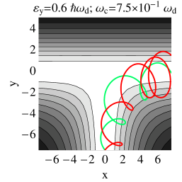
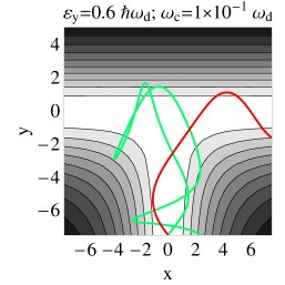
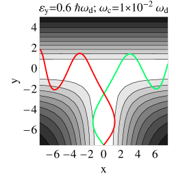
In order to show how the symmetry breaking produces a transverse current , we shortly discuss the case of a T-shaped junction, without SO term, in a uniform external magnetic field directed along : in Fig. 2 we report the corresponding classical electron trajectories. The increase of the magnetic field results in a broken symmetry between leads 2 and 4 and makes the probabilities of transmission in the two leads very different.
The current at lead of a multi-probe device can be expressed in terms of chemical potentials at each lead and of the transmission coefficient as ; normalization requires BL ; gei92 . Thus to an injected current in lead , it corresponds a transverse Hall current
This Hall current is mainly due to the electric field for and to the broken symmetry between leads and due to the magnetic field.
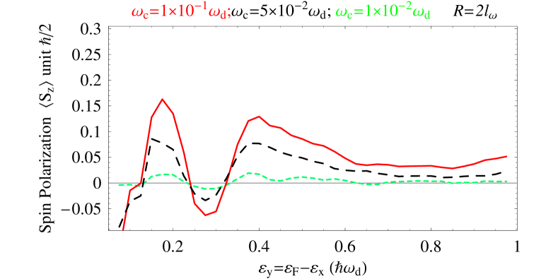
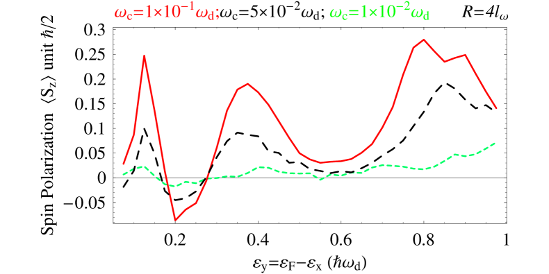
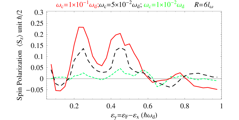
Spin Orbit and Effective Magnetic Field - In Fig. 3 we report the spin polarization of the transverse current, when considering a vanishing external magnetic field and a -coupling SO term. Numerical calculations are performed using the procedure discussed above. Thus, we show the spin polarization of the current flowing along the direction. corresponds to
in this special case where , because of the commutation between and and , since the effective magnetic field depends on the spin orientation of electrons injected in 1.
Starting from the number of trajectories we are able to estimate the statistical fluctuation on the calculated ,
where we take according to the binomial distribution.
Notice that, for between and , there is an inversion of the spin polarization () for each panel of Fig. 3. It is well known that a strong geometry dependence of the transport properties was shown in the presence of a transverse magnetic field by giving negative Hall current, as we discussed above concerning the ”quenching of the Hall effect”. In fact, the resistances measured in narrow-channel geometries are mainly determined by the scattering processes at the junctions with the side probes which depend strongly on the junction shape ref289 . This dependence of the low-field Hall current was demonstrated ref358 and measured fordbvh . In a recent papernoiq was discussed how the effective field generated by the -SOC characterizes a regime of transport that can be assumed as the quenching regime of the SHE. Hence, it follows that the inversion of the spin polarization, shown in Fig. 3, can be explained on the same ground. Moreover, this behaviour has a clear signature around while for other values of the Fermi energy the calculated quenching is comparable with the statistical fluctuation due to the numerical approach.
The geometry dependence of can be clearly inferred by comparing the three panels of Fig. 3, where we show the effects of the width of the crossing region (). We can conclude that a significant spin polarization of the transverse current can be obtained at some fixed values of the Fermi energy, and that a more efficient process is given by the junction with , while can be attenuated in larger or smaller junctions.
By comparing Fig. 2 and Fig. 4, where some trajectories are shown, we can understand the microscopic mechanism which produces the transverse spin current, by focusing on the symmetry breaking between the spin-up and spin-down electrons.
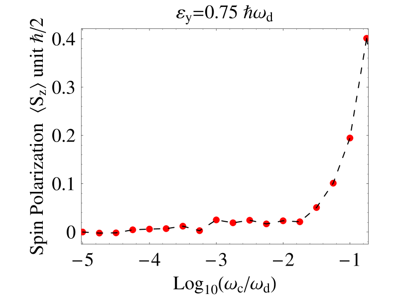
In order to evaluate the order of magnitude corresponding to the spin polarization, we can calculate the dependence of on the strength of the -SOC. In Fig. 5 we show the value of the spin polarization, as it can be measured at lead 2, for different strengths of coupling ranging over 5 orders of magnitude.
We distinguish two cases according to the possibilities that in lead is injected, respectively: (i) a non polarized current or (ii) a polarized charge current. In case (i), there is no charge current between leads and , but a pure spin current, , that is proportional to . This quantity can also be read as the spin polarization of the current in the lead 2, when an unpolarized spin current is injected in the lead 1. Fig. 3 shows that, for some energies, this spin current quenches and eventually reverses its sign. The same is observed for a fixed value of the energy, when changing the parameter (different values of could be experimentally obtained by changing the value of the effective width of the wires defining the T-junction, or by changing the value of the coupling parameter). This phenomenon has been treated in a recent papernoiq studying the transport through micrometric ballistic 4-probe X-junctions, where it was found that this magneto-transport anomaly is closely related to the quenched or negative Hall resistance. In case (ii) a charge current flows between leads 2 and 4, as can be seen considering a completely polarized injected current (e.g. having all electrons with spin up). In that case will be proportional to a charge current flowing between leads 2 and 4. It is easy to see that, even if the current is not completely polarized, there will be a charge current flowing between leads 2 and 4 that is proportional to the polarization degree of the injected current,
where is the charge conductance, and is the spin polarization of the injected current. This scheme would implement the electric detection of a spin polarized current.
Conclusion - We described a system based on the SO -coupling capable of spin filtering and electric based spin polarization measurements. The results we have shown were obtained using values of and well within those given by presently available 2DEGs and nanolithography techniques. The use of a series of T nanojunctions could also give some better results in the spin polarization of the emerging current.
The proposed devices also represent a new test for the effects of the -SO interactions which are at the basis of the quantum spin Hall effects recently discussed in several papersnoish ; qse ; iii ; hatt ; noiq . In these papers the -coupling was always assumed to be negligible, although in general this term is comparable to (or larger than) the -one. However, it can be shown that spin polarization effects of the coupling should be some orders of magnitude larger than the one calculated for the coupling with a comparable strengthnoiq .
References
- (1) D.D. Awschalom, D. Loss and N. Samarth, Semiconductor Spintronics and Quantum Computation (Springer, Berlin, 2002); B. E. Kane et al., Nature 393, 133 (1998).
- (2) M. I. D’yakonov and V. I. Perel’, JETP Lett. 13, 467 (1971).
- (3) J. Sinova, D. Culcer, Q. Niu, N. A. Sinitsyn, T. Jungwirth, and A. H. MacDonald, Phys. Rev. Lett. 92, 126603 (2004).
- (4) J. E. Hirsch, Phys. Rev. Lett. 83, 1834 (1999).
- (5) E. M. Hankiewicz, L. W. Molenkamp, T. Jungwirth, and J. Sinova, Phys. Rev. B 70, 241301 (2004).
- (6) C. L. Kane and E. J. Mele, Phys. Rev. Lett. 95, 226801 (2005).
- (7) L. Sheng, D. N. Sheng, C. S. Ting, and F. D. M. Haldane, Phys. Rev. Lett. 95, 136602 (2005).
- (8) L. D. Landau, E. M. Lifshitz, Quantum Mechanics (Pergamon Press, Oxford, 1991).
- (9) Yu. A. Bychkov, E. I. Rashba, Pis’ma Zh. Eksp. Teor. Fiz. 39, 66 (1984) [JETP Lett. 39, 78 (1984)]).
- (10) M. J. Kelly Low-dimensional semiconductors: material, physics, technology, devices (Oxford University Press, Oxford, 1995).
- (11) S. Bellucci and P. Onorato, Phys. Rev. B 72, 045345 (2005); S. Bellucci and P. Onorato, Phys. Rev. B 68, 245322 (2003).
- (12) G. Engels, J. Lange, Th. Schäpers, and H. Lüth, Phys. Rev. B 55, R1958 (1997).
- (13) M. Schultz, F. Heinrichs, U. Merkt, T. Colin, T. Skauli, and S. Løvold, Semicond. Sci. Technol. 11, 1168 (1996).
- (14) S.-Q. Shen, Phys. Rev. Lett. 95, 187203 (2005).
- (15) B. K. Nikolic, L. P. Zarbo, and S. Welack, Phys. Rev. B 72, 075335 (2005).
- (16) B. Zhou, L. Ren, and S.-Q. Shen, Phys. Rev. B 73, 165303 (2006).
- (17) A. Berard and H. Mohrbach, Phys. Lett. A 352, 190 (2006).
- (18) T. J. Thornton, M. Pepper, H. Ahmed, D. Andrews, G. J. Davies, Phys. Rev. Lett. 56, 1198 (1986).
- (19) A. V. Moroz and C. H. W. Barnes, Phys. Rev. B 61, R2464 (2000).
- (20) S. Bellucci and P. Onorato, Phys. Rev. B 73, 045329 (2006).
- (21) B. A. Bernevig and S.-C. Zhang, Phys. Rev. Lett. 96, 106802 (2006).
- (22) Y. Jiang and L. Hu, cond-mat/0603755.
- (23) Kiminori Hattori and Hiroaki Okamoto, Phys. Rev. B 74, 155321 (2006).
- (24) S. Bellucci and P. Onorato, Phys. Rev. B 74, 245314 (2006).
- (25) A. A. Kiselev and K. W. Kim, Appl. Phys. Lett. 78, 775 (2001).
- (26) S. E. Laux, D. J. Frank, F. Stern, Surf. Sci. 196, 101 (1988); H. Drexler et al., Phys. Rev. B49, 14074 (1994); B. Kardynałet al., Phys. Rev. B55, R1966 (1997).
- (27) F. Carillo, G. Biasiol, D. Frustaglia, F. Giazzotto, L. Sorba, F. Beltram, Phys. E 32, 53 (2006).
- (28) X. C. Zhang, A. Pfeuffer-Jeschke, K. Ortner, V. Hock, H. Buhmann, C. R. Becker, and G. Landwehr, Phys. Rev. B 63, 245305 (2001).
- (29) M. Knop, M. Richter, R. Maßmann, U. Wieser, U. Kunze, D. Reuter, C. Riedesel and A. D. Wieck Semicond. Sci. Technol. 20, 814 (2005).
- (30) M. Büttiker Phys. Rev. Lett. 57, 1761 (1986).
- (31) T. Geisel, R. Ketzmerick and O. Schedletzky, Phys. Rev. Lett. 69, 1680 (1992).
- (32) C. J. B. Ford, S. Washburn, M. Büttiker, C. M. Knoedler, J. M. Hong, Phys. Rev. Lett. 62, 2724 (1989).
- (33) G. Timp, H. U. Baranger, P. deVegvar, J. E. Cunningham, R. E. Howard, R. Behringer, P. M. Mankiewich, Phys. Rev. Lett. 60, 2081 (1988).
- (34) H. U. Baranger, A. D. Stone, Phys. Rev. Lett. 63, 414 (1989).