Engineering Silicon Nanocrystals: Theoretical study of the effect of Codoping with Boron and Phosphorus
Abstract
We show that the optical and electronic properties of nanocrystalline silicon can be efficiently tuned using impurity doping. In particular, we give evidence, by means of ab-initio calculations, that by properly controlling the doping with either one or two atomic species, a significant modification of both the absorption and the emission of light can be achieved. We have considered impurities, either boron or phosphorous (doping) or both (codoping), located at different substitutional sites of silicon nanocrystals with size ranging from 1.1 nm to 1.8 nm in diameter. We have found that the codoped nanocrystals have the lowest impurity formation energies when the two impurities occupy nearest neighbor sites near the surface. In addition, such systems present band-edge states localized on the impurities giving rise to a red-shift of the absorption thresholds with respect to that of undoped nanocrystals. Our detailed theoretical analysis shows that the creation of an electron-hole pair due to light absorption determines a geometry distortion that in turn results in a Stokes shift between adsorption and emission spectra. In order to give a deeper insight in this effect, in one case we have calculated the absorption and emission spectra going beyond the single-particle approach showing the important role played by many-body effects. The entire set of results we have collected in this work give a strong indication that with the doping it is possible to tune the optical properties of silicon nanocrystals.
pacs:
73.22-f, 71.15-m, 78.55.-m; 78.20.-e.I Introduction
Bulk silicon is an indirect band-gap material emitting in the infrared region. Radiative lifetimes of excited carrier are very long, causing a predominant de-excitation via fast non-radiative recombinations. Moreover, silicon has a significant free carrier absorption and Auger recombination rates which makes the use of this material in optoelectronic applications very problematic.
During the last decade, several breakthroughs have increased the hopes of using nanostructured silicon as an optical active material.ossobook ; ossobori The basic idea has been to take advantage of the reduced dimensionality of the nanocrystalline phase (1-5 nm in size) where quantum confinement, band folding and surface effects play a crucial role.ossobook ; bisi Indeed, it has been found that Si nanocrystals band-gap increases with decreasing size with a luminescence external efficiency in excess of 23%.ossobook ; bisi ; gelloz Moreover, optical gain has been already demonstrated in a large variety of experimental conditions.pav1 ; pav2 ; pav3 ; pav4 ; lute Nevertheless, Si nanocrystals (Si-nc) still have a memory of the indirect band gap of the bulk phase and this is evidenced by the clearly observed structures related to momentum-conserving phonons.ossobook ; canh ; del2 This drawback can be circumvented by introducing an isoelectronic impurities. ossobook ; bisi Indeed, in a series of recent very interesting papers, Fujii and collaborators fujii3 ; fujii1 ; fujii2 have proved the possibility of a detailed control of the Si-nc photoluminescence by the simultaneous doping with n- and p- type impurities. In particular, they have showed that a (B and P) codoped Si-nc always has an higher photoluminescence intensity than that of both a single (B or P) doped and of an undoped nanocrystal. Besides, under resonant excitation condition, the codoped samples did not exhibit structures related to momentum-conserving phonons suggesting that, in this case, the quasi-direct optical transitions are predominant.fujii3 ; fujii1 ; fujii2
From a theoretical point of view, investigations of impurities in silicon nanostructures are very few when compared to the large number of papers reporting calculations for pure, undoped systems; moreover, most of them are based on semi-empirical approaches. An handful number of first-principles studies has been devoted to quantum confinement effects in single-doped Si-nc.melnikov ; cantele ; zhou ; ferna These works have basically shown that i) the Si-nc ionization energy is virtually size independent, ii) the impurity formation energy is greater for smaller nanocrystals and iii) impurity segregation strongly affects the conductance properties of nanostructures.melnikov ; cantele ; zhou ; ferna
We have recently started a systematic study of the electronic and optical properties of codoped Si-nc. Our first results feffe show that codoped Si-nc undergo a minor structural distortion around the impurities and that the formation energies are always smaller than those of the corresponding single-doped cases. Moreover, we have found that codoping reduces the band-gap with respect to the undoped nanocrystals, showing the possibility of an impurity based engineering of the Si-nc optical properties.feffe ; ossofeffe
We report here a comprehensive theoretical study of the structural, electronic and optical properties of B and P simultaneously doped Si nanocrystals using ab initio Density Functional Theory. The paper is organized as follows. Section II is focused on the description of the theoretical and computational methods, section III is dedicated to the discussion of our results. The results will be presented and discussed in the following order: i) structural properties (subsection III.1), ii) formation energies (subsection III.2) and iii) electronic (subsection III.3) and iv) optical properties (subsection III.4) for all the considered Si nanocrystals. Concerning the optical properties we discuss both absorption and emission spectra obtained within a single-particle approach (III.4.1) and, in one case, with many-body methods considering self-energy corrections and the Bethe-Salpeter scheme (III.4.2). Finally, in section IV we summarize our results.
II Computational Methods
Our results are obtained within a plane-wave
pseudopotential DFT scheme, using the Quantum-ESPRESSO package
pwscf . The impurity states are calculated in an
approximately spherical Si-nc, built by considering all the bulk
Si atoms contained in a sphere (centered on a Si ion) with a
diameter ranging from 1.1 nm (Si35H36) to 1.79 nm
(Si147H100). The surface dangling bonds are saturated
with hydrogens. Following the work of Fujii et al. fujii3 ,
we have located the B and P impurities in substitutional positions
just below the nanocrystal surface. It is worth mentioning that
this arrangement represents the most stable configuration, as
confirmed by theoretical and experimental
works.feffe ; colombi ; Garrone Full relaxation with respect to
the atomic positions has been allowed for both doped and undoped
systems. All the DFT calculations are performed within the
generalized gradient approximation (GGA) using Vanderbilt
ultrasoft vanderbilt pseudopotentials for the determination
of both the structural and electronic properties (see Sec.
III.1, Sec. III.2 and Sec. III.3) whereas
norm-conserving pseudopotential within the Local Density
Approximation (LDA) at the relaxed geometry have been used to
evaluate the optical properties (see Sec. III.4). This choice
is due to the fact that although Vanderbilt ultrasoft
pseudopotentials allow the treatment of several hundreds of atoms
per unit cell in the atomic relaxation process, the removal of the
norm-conservation condition is a well known problem for the
calculation of the optical transition matrix elements
check . Each nanocrystal has been placed in a large
supercell in order to prevent interactions between the periodic
replicas (about 6 Å of vacuum separates neighbor
nanocrystals). Structural, electronic and optical properties, as
well as the impurity formation energies, are investigated as a
function of the size and for several impurity positions within the
Si-nc. Starting from the SinHm nanocrystal,degoli the
formation energy of the neutral B or/and P impurities can be
defined as the energy needed to insert one B or/and one P atom
within the nanocrystal after removing one/two Si atoms
(transferred to the chemical reservoir, assumed to be bulk Si)Zhang
| (1) |
where E is the total energy of the system, the total energy per atom of bulk Si and the total energy per atom of the impurity (we consider the total energy per atom in the tetragonal B50 crystal for B, as in Ref. muB, and the orthorhombic black phosphorus for P, as in Ref. muP, ). The integers and can be set to either or . In particular, is the choice when a B impurity is present in the nanocrystal ( otherwise) and for a P impurity ( otherwise). With this prescription, Eq.1 can be used for both the single doping and the codoping case.
The calculations of the optical properties have been done both in the ground and in the first excited states, where the excited state corresponds to the electronic configuration in which the highest occupied single-particle state (HOMO) contains a hole, while the lowest unoccupied single-particle state (LUMO) contains the corresponding electron.franceschetti ; puzder ; onida ; leo It is worth pointing out that an undoped and relaxed Si-nc have Td symmetry; in the presence of doping, this high symmetry is generally lost due to the presence of the impurity atoms. Moreover, because of the significant differences in the charge density of the ground and excited states, the actual atomic relaxations in the two cases are different.
The nanocrystal optical response is evaluated for both the ground and the excited state relaxed geometries computing the imaginary part of the dielectric function () through the Fermi golden rule. The emission spectra have been calculated using the excited state atomic positions and the ground state electronic configuration (more details can be found in section III.4.2). It should be noted that although should only be used for calculating the nanocrystal absorption coefficient, it can also be used for getting a first approximation to the emission spectra simply because the emission can be viewed as the time reversal of the absorption.bassani In other words, once the relaxed atomic positions corresponding to to an hole in the HOMO and an electron in the LUMO have been found, these atomic positions are used for the calculation of whose main features are also those of the emission spectra. It is worth mentioning that the photoluminescence spectra can be derived using the well known Van Roosbroeck and Shockley shockley relation which, again, involves . However, such a calculation requires the knowledge of the electron and hole populations, at the working temperature, in the LUMO and HOMO states respectively. The populations, in turn, depends on the actual dynamics in the excitation and emission processes, including the non radiative electron hole recombinations. In this work we have not considered any particular dynamics so that our emission spectra contains only the informations related to both the transition energies and the oscillator strengths.
| Si87H76 | Si86BH76 | Si86PH76 | Si85BPH76 | ||
|---|---|---|---|---|---|
| Bond | Å | Bond | Å | Å | Å |
| Si-Sis | 2.355 | B-Sis | 2.036 | 2.021 | |
| Si-Sis | 2.355 | B-Sis | 2.036 | 2.021 | |
| Si-Sii | 2.363 | B-Sii | 2.014 | 2.034 | |
| Si-Sii | 2.363 | B-Sii | 2.014 | 2.034 | |
| Si-Sis | 2.355 | P-Sis | 2.294 | 2.295 | |
| Si-Sis | 2.355 | P-Sis | 2.294 | 2.295 | |
| Si-Sii | 2.363 | P-Sii | 2.380 | 2.331 | |
| Si-Sii | 2.363 | P-Sii | 2.380 | 2.331 |
In the case of the Si33BPH36 codoped Si-nc, going beyond the single-particle approach, we have included the self-energy corrections by means of the GW approximation.hedin In a successive step, excitonic effects are include solving the Bethe-Salpeter equation.onida A further advantage of this procedure is that the inhomogeneity of the system is taken into account by properly including local fields effects.tra1 This approach, in which many-body effects are combined with a study of the structural distortion due to the impurity atoms in the excited state, allows a precise determination of the Stokes shift between absorption and emission spectra.leo
III Results
This section collects all the results we have obtained in the study of the structural, electronic and optical properties of boron and phosphorus codoped silicon nanocrystals. When possible our outcomes are compared with available experimental results.
III.1 Structural Properties
First of all, it is interesting to look at the change in the nanocrystal structure induced by the presence of the impurities. As outlined above, the B or/and P impurity atoms have always been located in substitutional sites in the Si shell just below the surface, these positions having previously been shown to be the most stable ones.cantele Initially, we have considered impurities located on opposite sides of the nanocrystals, thus at the largest possible distance.
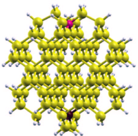
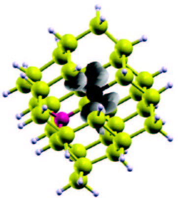
Table I gives the relaxed bond lengths around the impurities for Si87H76 whose structure is shown in Fig.1.
Comparing these bond lengths with those of the corresponding Si atoms in the undoped Si-nc it is clear that some significant relaxation occurs around the impurities. In all the cases the local structure has a symmetry, with two shorter and two longer Si-impurity bonds with respect to the two surface and the two inner Si atoms. An interesting point is that the amount of relaxation around the impurity is directly related to the impurity valence. The most significant relaxation is found for the trivalent atom (B, 2.036 and 2.014 Å with respect to 2.355 and 2.363 Å) to be compared with that of the pentavalent one (P, 2.294 and 2.380 Å with respect to 2.355 and 2.363 Å). Besides, it is interesting to note that in the codoped case the differences among the four impurity-Si bond lengths are always smaller than the single-doped case (the Si-B bonds differ of about 1.08% in the single-doped case and only 0.64% in the codoped case, whereas this variation in the case of P reduces from 3.61% to 1.54%). Thus, if carriers in the Si-nc are perfectly compensated by simultaneous n- and p-type doping, an almost configuration is recovered.
| Si35H36 | Si34BH36 | Si34PH36 | Si33BPH36 | ||
|---|---|---|---|---|---|
| Bond | Å | Bond | Å | Å | Å |
| Si-Sis | 2.300 | B-Sis | 2.093 | 2.035 | |
| Si-Sis | 2.300 | B-Sis | 2.022 | 2.026 | |
| Si-Sis | 2.300 | B-Sis | 2.022 | 2.026 | |
| Si-Sii | 2.361 | B-Sii | 2.008 | 2.007 | |
| Si-Sis | 2.300 | P-Sis | 2.366 | 2.303 | |
| Si-Sis | 2.300 | P-Sis | 2.365 | 2.302 | |
| Si-Sis | 2.300 | P-Sis | 2.364 | 2.297 | |
| Si-Sii | 2.361 | P-Sii | 2.310 | 2.334 |
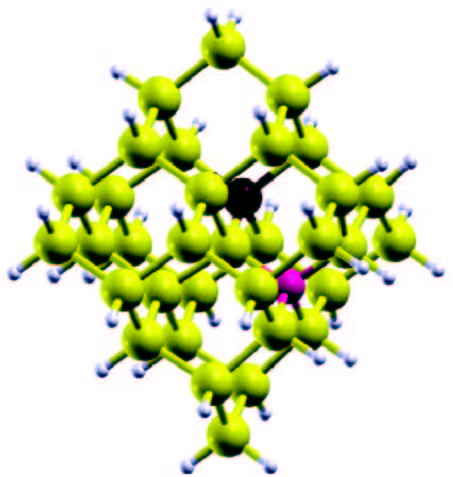
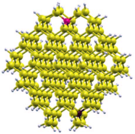
This tendency towards a symmetry of codoped Si-nc is also obtained for smaller and larger nanocrystals, showing that these outcomes are independent of the Si-nc size. Anyway, a symmetry lowering with respect to Si87H76 is present due to the different neighborhood experienced by the impurities. It should, in fact, be noted that in the case of Si35H36 and Si147H100 the atoms in the first subsurface shell are bonded to three surface Si atoms and to one inner Si atom, while for Si87H76 they are bonded to two surface and to two inner Si atoms. The impurity positions for the considered nanocrystals are showed in Fig. 1, Fig. 2 and Fig. 3.
| Si147H100 | Si146BH100 | Si146PH100 | Si145BPH100 | ||
|---|---|---|---|---|---|
| Bond | Å | Bond | Å | Å | Å |
| Si-Sis | 2.356 | B-Sis | 2.029 | 2.016 | |
| Si-Sis | 2.356 | B-Sis | 2.029 | 2.016 | |
| Si-Sis | 2.356 | B-Sis | 2.063 | 2.018 | |
| Si-Sii | 2.369 | B-Sii | 2.009 | 2.022 | |
| Si-Sis | 2.356 | P-Sis | 2.310 | 2.306 | |
| Si-Sis | 2.356 | P-Sis | 2.310 | 2.306 | |
| Si-Sis | 2.356 | P-Sis | 2.372 | 2.338 | |
| Si-Sii | 2.369 | P-Sii | 2.321 | 2.321 |
Table II and III give the structural modifications that occur around the impurities for Si35H36 and Si147H100, respectively. Even in these cases the differences between the four Si-impurity bond lengths on going from the undoped to the single-doped to the codoped case first increase and then decrease.
Once stated that the amount of structural deformation remains unvaried as the nanocrystal size changes and having shown that this behavior is simply related to the codoping, we have devoted our attention on how the presence of both the impurities acts. We have looked, in particular, at what happens to the impurity-impurity distance when compared to the corresponding Si-Si distance in the undoped nanocrystal.
We have calculated these distances for Si145BPH100 keeping the B atom fixed in a subsurface position and moving the P atom through different substitutional sites along the first subsurface shell, as schematically shown in Fig. 4.
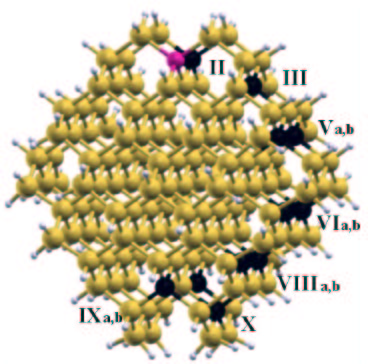
We have moved the P atom from the position labeled II to the positions III, V-a, V-b, VI-a, VI-b, VIII-a, VIII-b, IX-a, IX-b and X. Here roman number refers simply to the positions evidenced in Fig. 4. For each configuration, we have calculated the B-P distance after a geometry relaxation and repeated the calculation for the corresponding Si-Si distance. The results are shown in Fig. 5 where, as a reference, we also show the corresponding distances in bulk silicon.
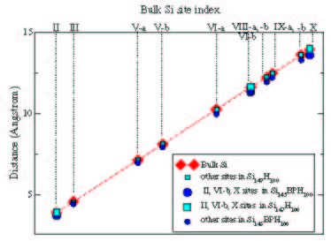
Taking bulk silicon as a reference, values above the dashed line reflect an increase whereas values below correspond to a reduction of the distances. It is seen that in all the cases considered the distances are only weakly modified. Indeed, on going from the undoped nanocrystals (where the distances are almost the same as in bulk silicon) to the codoped ones we note a very small shrinkage of the impurity-impurity distances. This shows, once again, that if carriers are perfectly compensated by simultaneous doping, the Si-nc does not really undergoes a significant structural distortion, and this fact does not depend on the distance between the impurities.
III.2 Formation energy
The different structural deformations occurring in the single-doped and codoped nanocrystals around the impurity (see Tables I, II and III) have a deep influence on the stability of the analyzed systems. As stated in Sect. II, starting from SinHm,degoli the formation energy of the neutral B or/and P impurities can be defined as the energy needed to insert one B or/and one P atom within the nanocrystal after removing one/two Si atoms.
In order to clarify which are the parameters that play an important role in the determination of the formation energy, we have performed a series of total energy calculations considering: i) single-doped and codoped nanocrystals, ii) nanocrystals of different sizes, iii) impurities located in different sites and iv) variable impurity-impurity distance within a nanocrystal.
In Fig. 6 we report the calculated formation energies of Si35H36 (diameter d= 1.10 nm), Si87H76 (d= 1.50 nm) and Si147H100 (d = 1.79 nm).
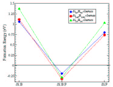
In the same figure, as a reference, we report also the single-doping formation energies. For the codoped case, B and P impurities have been placed as second neighbors. This choice corresponds to the nearest possible distance between two subsurface sites for both Si33BPH36 (see Fig. 2) and Si145BPH100 (see the position labeled II in Fig. 4)). After a geometry relaxation, the distances between B and P impurities are D = 3.56 Å, D = 3.64 Å and D = 3.68 Å for Si33BPH36, Si85BPH76 and Si145BPH100 respectively.
From Fig. 6 it is clear that the simultaneous B and P doping strongly reduces (of about 1 eV) the formation energy with respect to both B and P single-doped cases and that this reduction is similar for Si-nc of different sizes. Thus, while B or P single doping is very costly (in particular, the formation energy increases with decreasing the nanocrystals size, in agreement with previous calculations melnikov ; cantele ), the codoping is much easier and, as a good approximation, independent of the nanocrystal size. The important point here is that Si-nc can be more easily simultaneously doped than single-doped; this is due to both the charge compensation and to the minor structural deformation.
It is interesting to look at the detailed dependence of the formation energy on the distance between the two impurities. In Fig. 7 we present the comparison between the formation energies of Si85H76 and Si145H100 with impurities placed at two different distances : 1) the previous considered second neighbors ones and 2) the largest possible impurities distance (D = 10.60 Å and D = 13.29 Å for the Si85BPH76 and Si145BPH100 respectively, see Fig. 1 and Fig. 3).
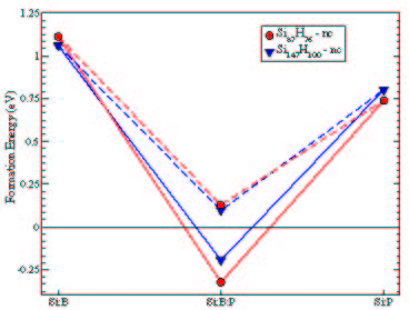
We note that when the impurity-impurity distance is reduced, the formation energy decreases of 0.2-0.3 eV taking negative values. This fact demonstrates that a stronger interaction between impurities leads to a reduction in the formation energy, so that codoping result to be easier and more likely when the dopants are closer to each other. In the latter case, the reduction of the formation energy is almost independent of the nanocrystal size, as shown in Fig. 6.
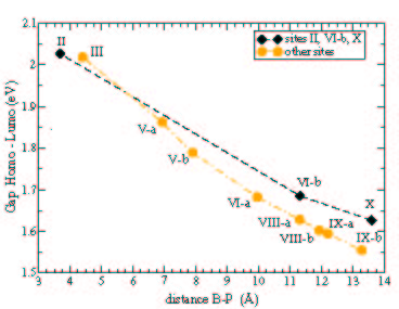
In order to investigate in more detail the dependence of the formation energy on the impurity-impurity distance, we focus our attention on the codoped Si145BPH100, trying to trace a “formation energy path” by progressively increasing the B-P distance. In this calculation we have kept the B atom frozen in a subsurface position while moving the P atom through different substitutional sites along the first subsurface shell, as schematically sketched in Fig. 4. The results of these calculations are shown in Fig. 8.
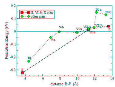
Two interesting effects are evidenced in this figure. The first one is that the formation energy assumes a negative value when the impurities are placed at distances smaller than 10 Å, evolving towards positive values for larger distances. This change of sign can lead to the definition of a “critical impurity distance”. Below such a threshold the interaction between boron and phosphorus is strong and gives rise to a reduction of the formation energy. On the contrary, above this value, the interaction tends to be quenched reducing the stability of the impurity complex.
These considerations are also supported by Fig. 9 where we report the values of the formation energy for three different nanocrystals in which the impurities are always located in the subsurface shells at different distances.
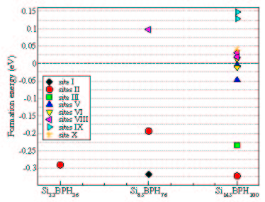
As before, it is evident from this figure that the distance between impurities plays a fundamental role on the decrease of the formation energy. For each nanocrystal, the formation energy takes on negative values below a given distance. Moreover, the formation energy have a minimum value when the impurities are located at the minimum possible distance. Indeed, the impurity-impurity distance seems to play a major role with respect to the nanocrystals size, since the formation energy for similar impurity configurations are quite independent of the nanocrystal dimension. The small difference between the Si85BPH76 and the Si33BPH36 and Si145BPH100 is due to the different neighborhood experienced by the impurities in the three cases (see Tables I, II and III).
Another relevant point is the possibility to identify two distinct trends for the formation energy (see Fig. 8) that can be related to the type of silicon cage surrounding the P dopant site. One can group (dotted line) together the cases in which the P impurity is located in the positions labeled II, VI-b and X with respect to the B impurity (see Fig. 4). In these positions two of the surface Si atoms bounded to the P impurity present two passivating H atoms instead of one, a situation that dominates in all the other configurations. A different number of capping H atoms influences the formation energy.
III.3 Electronic Properties
In this section we will investigate the role of codoping on the electronic properties of Si-nc. As in the corresponding bulk system, the insertion of impurities tends to modify the electronic structure. We shall show that, by properly controlling the doping and the size, it is possible to modulate both the electronic structure and some optical features. In particular, we shall show how the electronic properties of the codoped nanocrystals depend on both the nanocrystal size and on the distance between the impurities. Some of the results will be discussed in terms of wave function localization around the impurity complex.
In the single-doped cases we have already shown that the presence of either donor or acceptor states can considerably lower the energy gap (EG, the HOMO-LUMO energy difference) of the undoped Si-nc,cantele ; feffe defining in this case the energy gap as the gap between the impurity level (partially filled considered as the HOMO) and the LUMO (which is empty). In these cases the partially filled HOMO level is strongly localized either on the B or on the P impurity. For example, in the case of Si86BH76 the defect level is located just 0.28 eV above the valence band reducing the above defined energy gap from 2.59 eV (the value for the undoped Si-nc) to 2.31 eV. In Si86PH76 the defect level is located just 0.28 eV below the conduction band so that the energy gap is only 0.28 eV.feffe It is interesting to note that the experimental substitutional donor binding energy for P in bulk Si is about 33 meV, while the experimental acceptor energy for B in Si is 45 meV,cardona showing how, in the case of nanocrystals, the combined effects of both quantum confinement and weak screening tend to “transform” shallow impurities in “deep” centers.melnikov ; cantele ; ninno ; tra2
The electronic properties of B- and P- codoped Si-nc are qualitatively and quantitatively different from those of either B- or P- single-doped Si-nc. Now the system is a semiconductor and the presence of both the impurities leads to a HOMO level that contains two electrons and to a HOMO-LUMO energy gap strongly lowered with respect to that of the corresponding undoped nanocrystals. Fig. 10 shows the energy levels of Si147H100 and Si145BPH100 with the impurities located at two different distances.
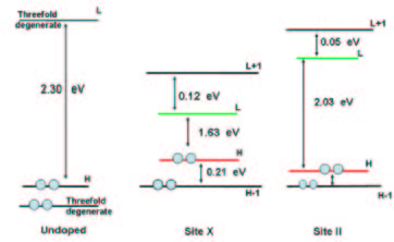
In one case, the impurities are placed at the largest possible distance (D = 13.29 Å) and in the other one at the already discussed minimum distance (D = 3.68 Å) for this particular nanocrystal. From the figure it is evident that when impurities are at the larger distance, EG is strongly reduced with respect to the corresponding undoped value (EG is lowered from 2.30 eV to 1.63 eV). On the contrary, when the impurities are close to each other, EG enlarges (EG = 2.03 eV) although it still remains below the undoped case. We can think that when impurities are brought closer, the Coulomb interaction becomes stronger so that the energy gap becomes larger. Boron and phosphorus feel each other like a B-P complexes with a gap opening recalling the DFT-LDA calculated gaps of the boron phosphide bulk system: direct gap 3.3 eV, indirect gaps ( ) 2.2 eV, and ( ) 1.2 eV, as described in Ref. bp, .
These behaviors are corroborated by the calculated HOMO and LUMO wave functions. Fig. 11 shows the square modulus contour plots of the HOMO and LUMO states of the two considered Si145BPH100 nanocrystals.
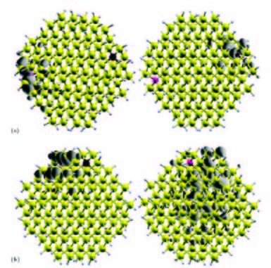
The top panel shows the contour when the impurities are at a large distance while the bottom panel is that with the impurities at short distance. It clearly appears from these contours that on going from the case with well separated impurities to the that with close impurities, the overlap between the HOMO, strongly centered on the boron atom, and the LUMO, mainly localized on the phosphorus atom, strongly increases.
Next we investigate how the electronic structure changes as a function of the impurity distance within the Si145BPH100 nanocrystal. In Fig. 12 we report the trend of the HOMO-LUMO energy gap with respect to the distance between impurities.
It is seen that the mutual impurity distance affects not only the formation energy (see Sec. III.2), but also the electronic structure. We observe that EG decreases almost linearly with the increase of the impurity distance; moreover, also in this case we can figure out the presence of two different trends related to the different surface region experienced by the P atom in the sites II, VI-b and X, with respect to the other ones (see also Fig. 8 and related discussion). Fig. 12 points out how, at least in principle, it is possible to tune EG as a function of the impurity-impurity distance. It is easy to predict that for Si-nc larger than those considered here it would be possible by codoping to obtain a energy gap even smaller than that of bulk Si.
The possibility of modulating the electronic properties of the codoped Si-nc is also evident if we keep the distance between the impurities constant and look at the dependence of the energy gap on the Si-nc size. Fig. 13 shows, for three different nanocrystals where the impurities are placed as second neighbors, how the undoped nanocrystal energy gap is reduced in the presence of codoping (see also Table IV).
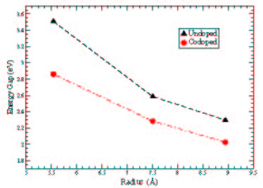
The same quantum confinement effect trend (i.e. larger gap for smaller nanocrystals) is observed for both the undoped and the codoped cases. Moreover, the energy gap of the codoped Si-nc is shifted towards lower energies with respect to that of the undoped EG; this shift is stronger for smaller nanocrystals. Playing with both the nanocrystal size and the distance between the impurities new interesting routes may be opened for optoelectronic applications.
| starting nc | d (nm) | EG undoped (eV) | EG codoped (eV) |
|---|---|---|---|
| Si35H36 | 1.10 | 3.51 | 2.86 |
| Si87H76 | 1.50 | 2.59 | 2.29 |
| Si147H100 | 1.79 | 2.30 | 2.03 |
Looking at the energy gap trends in Fig. 12 and Fig. 13 and considering that in the codoped case Fujii et al. fujii1 found photoluminescence peaks centered in the 0.9-1.3 eV energy region, we may conclude that Si-nc playing a role in the experiment have dimensions of the order of few nanometers. This conclusion is consistent with the experimental outcomes fujii1 that indicates an average nanocrystal diameter of about 5 nm.
III.4 Optical Properties
The aim of this section is to investigate the mechanisms involved in the modification of the optical properties of codoped Si nanocrystals. We present absorption and emission spectra with a comparison between the IP-RPA (independent particle-random phase approximation) spectra and the many-body ones. These last ones are obtained within a GW-BSE approach that takes into account not only the self-energy correction and the local field effects but also the electron-hole interaction. All the calculations performed are not spin-polarized. However it should be noted that single-particle calculations for undoped Si-nc have been done by Franceschetti and Pantelides franceschetti within the local spin-density approximation, showing that the singlet-triplet splitting is significantly smaller than the Stokes shift. To understand the role of dimensionality and impurity distance and to show the importance of including many-body effects in the optical spectra, we are going to present first the result of a RPA independent particle optical response for various codoped nanocrystals different in dimensions and in impurity location (see Sect. III.4.1), and next, we will present a complete study of a codoped Si-nc where we go beyond the single-particle approach within the GW-BSE framework (see Sect. III.4.2).
III.4.1 Absorption and emission spectra: single-particle results
We first discuss the results related to the absorption spectra. Fig.14 shows a comparison between the undoped Si87H76 and the codoped Si85BPH76 IP-RPA absorption spectra.
In this case the impurities are located at a distance of 10.60 Å. The optical response is evaluated for the ground state relaxed geometry computing the imaginary part of the dielectric function . It can be seen from Fig.14 that new transitions arise below the absorption onset of the undoped Si-nc. In particular, we have found a shift of the absorption gap to lower energies with respect to the undoped case toghether with an enhancement of the intensities around 2.0 eV. These new transitions are due to the presence of new HOMO and LUMO states localized on the impurities, as described in Sec. III.3 (see for example Fig. 11). The inset of Fig. 14 clarifies how the peak located in the 2.0-2.2 eV energy region is related to contributions that involve the HOMO-1, HOMO to LUMO, LUMO + 1 transitions; it should be noted that for all these levels the wavefunctions are predominantly localized on the impurities. If we compare these results with those of a single-doped Si-nc,feffelumin we note that the simultaneous presence of both impurities naturally suppresses all the absorption energy structures present in the infrared region (below 1 eV) of the single-doped spectra.
It is clear that, like the electronic properties, also the optical ones present a marked dependence on the nanocrystal dimension. To elucidate this point we plot in Fig. 15 the single-particle absorption spectra of three different Si-nc, the Si33BPH36, Si85BPH76, Si145BPH100, whose diameters are 1.10 nm, 1.50 nm and 1.79 nm, respectively. In all the three nanocrystals the impurities are second neighbors.
Two facts emerge from this figure. First of all, on increasing the nanocrystal size the absorption gap is strongly reduced (see arrows in Fig. 15). Second, an increase of the Si-nc diameter (i.e. a decrease of the impurity weight with respect to the total number of atoms) results in a lowering of the intensity for the transitions that involve the impurities.
The role of the impurity distance on the optical response has been investigated following the same approach adopted for the electronic properties in Sec. III.3. In Fig.16 the single-particle absorption spectra of Si145BPH100 are reported with P impurity placed on sites II, III, IX, and X respectively (see for comparison Fig. 4).
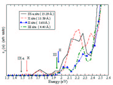
Here we observe a shift of the absorption gap to lower energy on increasing the distance between the impurities (see arrows in Fig. 16). Moreover, also the intensity is affected by the impurity distance. Stronger transitions arise when the impurities are closer whereas the intensity gets lower when the impurities are at a larger distances; the optical transitions near the band edge (indicated by arrows in Fig. 16) exhibit weaker oscillator strengths.
Now we discuss the results for the emission spectra and for the Stokes shift between absorption and emission. The nanoscrystal excitation has been studied considering the excited state as the electronic configuration in which the highest occupied single-particle state (HOMO) contains a hole (), while the lowest unoccupied single-particle state (LUMO) contains the corresponding electron (), thus simulating the creation of a electron-hole pair.godby ; frang ; weisskerprl90 ; puzder Initially the system is in its ground state and the electronic excitation occurs with the atomic positions fixed in this configuration. After the excitation, due to the change in the charge density, relaxation occurs until the atoms reach a new minimum energy due to the presence of the electron-hole pair. The new atomic positions modify the electronic spectrum, implying that the levels involved in the emission process change. This model assumes that the relaxation under excitation is faster than the electron-hole recombination. The difference between the absorption and emission energies due to the different atomic positions represents the nanocrystal Stokes shift.franceschetti ; leo ; comp
The calculations have been performed for two Si-nc of different sizes taking, in the larger Si-nc, the impurities located at different distances. As shown in Table V, both the absorption and emission HOMO-LUMO energies are affected by these two parameters.
| Si33BPH36 | Si85BPH76 | ||
|---|---|---|---|
| d (nm) | 1.10 | 1.50 | 1.50 |
| D (Å) | 3.56 | 2.00 | 10.60 |
| Abs. (eV) | 2.77 | 2.32 | 1.75 |
| Ems. (eV) | 1.78 | 2.20 | 1.36 |
| (eV) | 0.99 | 0.12 | 0.39 |
With regard to the first parameter, we note that the Stokes shift strongly depends on the size showing a strong decrease on increasing the diameter of the Si-nc. This is due to the fact that for larger nanocrystals the excitation determines a minor distortion of the geometry. Concerning the second parameter, we see that the Stokes shift tends to slightly increase with B-P distance although this effect is small if compared with the lowering due to the increase of the Si-nc dimensions. The comparison between these results and the ones previously obtained for undoped clusters (0.92 eV for the Si35H36-ncdegoli and 0.22 eV for the Si87H76-ncpuzder ) confirm that the Stokes shifts is mainly determined by the nanocrystals size, but that nevertheless it depend slightly on the presence of the impurities and also on their mutual distance.
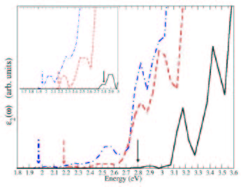
Looking at the single-particle optical spectra in Fig. 17 we note that the HOMO-LUMO transition in Si85BPH76 (1.75 eV, bottom panel) is almost dark when the two impurities are far apart and becomes instead allowed (2.32 eV, top panel) when their distance decreases. As discussed before, this oscillator strength enhancement is a consequence of the character of the HOMO and LUMO states in the two cases.
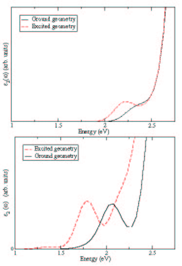
The emission (red-dashed lines in Fig. 17) spectra is red shifted with respect to the absorption (black-solid lines in Fig. 17). This red shift is a consequence of the geometry relaxation in the excited state due to the excess energy necessary for promoting of an electron in the LUMO level. The dependence of the emission spectra both on the nanocrystals size (see Table V and Fig. 15) and on the impurities positions (see Figs. 16 and 17) reveals once more the possibility of tuning the optical response of silicon nanocrystals.
III.4.2 Absorption and Emission Spectra: Many-body effects
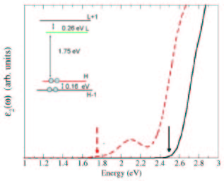
In order to give a complete description, within the many-body framework, of the codoped Si-nc response to an optical excitation, we consider both the self-energy corrections by means of the GW method GWdetails to obtain the quasiparticle energies and the excitonic effects through the solution of the Bethe-Salpeter equation. The effect of local fields is also included, to take into account the inhomogeneity of the systems.
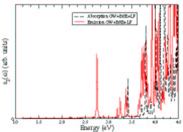
Since the GW-BSE calculation exccode are very computing demanding, we have only considered the smaller codoped nanocrystal Si33BPH36 (see Fig. 2). In this particular cluster, we found that Local fields effects are, although not negligible, of minor importance with respect to GW and excitonic effects. It is anyway essential to include all of them (LF and many-body) in order to get the final converged spectrum shown in Fig. 18.
In order to carry out emission spectra calculations, we use the excited state geometry and the ground state electronic configuration. As already noted before, in this case corresponds to an absorption spectrum in a new structural geometry. In other words, we consider the emission as the time reversal of the absorption.bassani ; leo Thus, the electron-hole interaction is here considered also in the emission geometry. The heavy GW-BSE calculation is made considering a large FCC supercell with a 50 a.u. lattice parameter. The correlation part of the self-energy has been calculated using 10081 plane waves, while 49805 plane waves have been used for the exchange part . Then, the full excitonic Hamiltonian is diagonalized considering more than 8000 transitions.
Fig. 18 shows the calculated absorption and emission spectra fully including the many-body effects. The electron-hole interaction yields significant variations with respect to the single-particle spectra (see for a comparison Fig. 17), with an important transfer of the oscillator strength to the low energy side. Moreover, in the emission spectrum the rich structure of states characterized, in the low energy side, by the presence of excitons with largely different oscillator strengths, determines excitonic gaps well below the optical absorption onset. Thus the calculated emission spectrum results to be red shifted to lower energy with respect to the absorption one. This energy difference between emission and absorption, the Stokes shift, can be lead back to the relaxation of the Si-nc after the excitation process.
The new important features that appear in the emission many-body spectra are related to the presence of both B and P impurities as showed by Fig. 19, which gives the real-space probability distribution for the bound exciton as a function of the electron position when the hole is fixed in a given position. In this case the hole is fixed on the boron atom and we see that the bound exciton is mainly localized around the phosphorus atom.
From Table VI, it can be seen that the single-particle DFT results strongly underestimate the absorption and emission edge with respect to the GW+BSE calculation, in which the excitonic effect are taken exactly into account. This means that, in this case, the cancellation between GW gap opening (which gives the electronic gap) and BSE gap shrinking (which originates the excitonic gap) is only partial.del
The difference between the GW electronic gap and the GW+BSE optical excitonic gap gives the exciton binding energy Eb. We note the presence of exciton binding energies as big as 2.2 eV, which are very large if compared with bulk Si ( 15 meV) or with carbon nanotubesspataru ; chang where E 1 eV, but similar to those calculated for undoped Si-nc leo of similar size and for Si and Ge small nanowires.bruno1 ; bruno2
| Si33BPH36 | DFT | GW | GW+BSE |
|---|---|---|---|
| Abs. (eV) | 2.80 | 5.52 | 3.35 |
| Ems. (eV) | 1.79 | 4.37 | 2.20 |
| (eV) | 1.01 | 1.15 | 1.15 |
The differences between full many-body calculations and single-particle results are of 0.55 eV and 0.41 eV for absorption and emission energy gaps respectively, and of 0.14 eV between the two Stokes shifts. It is interesting to note that the HOMO-LUMO transition in the emission spectrum at 2.20 eV is almost dark while an important excitonic peak is evident at about 2.75 eV (see Fig. 18), again red-shifted with respect to the first absorption peak. As expected, what comes out is the importance of fully taking into account the many-body aspect of the problem in order to overcome the limits of the single-particle approach.
IV Conclusions
The structural, electronic and optical properties of Si nanocrystals codoped with B and P impurities have been studied also going beyond the single-particle approach. We have considered Si-nc of different size and with the impurities located at different distances. We show that codoping is always energetically favored with respect to simple B- or P-doping and that the two impurities tend to occupy nearest neighbor sites near the surface rather than other positions inside the nanocrystal itself. Our results demonstrate that the codoped nanocrystals present valence and conduction band-edge states which are localized on the two impurities respectively and band-gaps always lower in energy with respect to that of undoped Si nanocrystals. Besides, the electronic properties show a dependence on both nanocrystal size and impurity-impurity distance. The impurity located band-edge states originate absorption thresholds in the visible region which are shifted lower in energy with respect to the undoped case. Moreover, the emission spectra show a Stokes shift with respect to the absorption which is due to the structural relaxation after the creation of the electron-hole pair. Our results make evident the presence of electronic quasi-direct optical transitions between donor and acceptor states that can help to understand the experimental outcomes and makes it possible to engineer the absorption and emission properties of Si nanocrystals.
Acknowledgments
We acknowledge the support of the MIUR PRIN (2005) Italy, of the CNR-CNISM ”Progetto Innesco” of the CRUI Vigoni Project (2005-2006) Italy-Germany and of EU Nanoquanta Network of Excellence (NMP4-CT-2004-500198). All the calculations were performed at CINECA-Bologna (”Iniziativa Calcolo Parallelo del CNR-INFM”), CICAIA-Modena and “Campus Computational Grid”-Università di Napoli “Federico II”.
References
- (1) S. Ossicini, L. Pavesi, and F. Priolo, Light Emitting Silicon for Microphotonics, Springer-Berlin (2003).
- (2) V. N. Borisenko and S. Ossicini, What is What in the Nanoworld, Wiley-VCH, Weinheim (2004).
- (3) O. Bisi, S. Ossicini, and L. Pavesi, Surf. Sci. Reports 38, 5 (2000).
- (4) B. Gelloz, A. Kojima, and N. Koshida, Appl. Phys. Lett. 87, 031107 (2005).
- (5) L. Pavesi, L. Dal Negro, C. Mazzoleni, G. Franzó, and F. Priolo, Nature 408, 440 (2000).
- (6) L. Dal Negro, M. Cazzanelli, L. Pavesi, S. Ossicini, D. Pacifici, G. Franzó, and F. Priolo, Appl. Phys. Lett. 82, 4636 (2003).
- (7) J. Ruan, P. M. Fauchet, L. Dal Negro, M. Cazzanelli, and L. Pavesi, Appl. Phys. Lett. 83, 5479 (2003).
- (8) M. Cazzanelli, D. Kovalev, L. Dal Negro, Z. Gaburro, and L. Pavesi, Phys. Rev. Lett. 93, 207042 (2004).
- (9) K. Luterová, K. Dohnalová, V. Šervček, I. Pelant, J.-P. Likforman, O. Crégut, P. Gilliot, and B. Hönerlage, Appl. Phys. Lett. 84, 3280 (2004).
- (10) Properties of Porous Silicon, ed. by L. T. Canham (IEE INSPEC, London 1997).
- (11) C. Delerue, G. Allan, and M. Lannoo, Phys. Rev. B 64, 193402 (2001).
- (12) M. Fujii, Y. Yamaguchi, Y. Takase, K. Ninomiya, and S. Hayashi, Appl. Phys. Lett. 87, 211919 (2005).
- (13) M. Fujii, K. Toshikiyo, Y. Takase, Y. Yamaguchi, and S. Hayashi, J. Appl. Phys. 94, 1990 (2003).
- (14) M. Fujii, Y. Yamaguchi, Y. Takase, K. Ninomiya, and S. Hayashi, Appl. Phys. Lett. 85, 1158 (2004).
- (15) D. V. Melnikov and J. R. Chelikowsky, Phys. Rev. Lett. 92, 046802 (2004).
- (16) G. Cantele, E. Degoli, E. Luppi, R. Magri, D. Ninno, G. Iadonisi, and S. Ossicini, Phys. Rev. B72, 113303 (2005).
- (17) Z. Zhou, M. L. Steigerwald, R. A. Friesner, L. Brus, and M. S. Hybertsen, Phys. Rev. B71, 245308 (2005).
- (18) M. V. Fernández-Serra, Ch. Adessi, and X. Balse, Phys. Rev. Lett. 96, 166805 (2006).
- (19) S. Ossicini, E. Degoli, F. Iori, E. Luppi, R. Magri, G. Cantele, F. Trani, and D. Ninno, Appl. Phys. Lett. 87, 173120 (2005).
- (20) S. Ossicini, F. Iori, E. Degoli, E. Luppi, R. Magri, R. Poli, G. Cantele, F. Trani, and D. Ninno, J. Select. Topics in Quantum Electr. 12, 1585 (2006).
- (21) S. Baroni, A. Dal Corso, S. de Gironcoli, P. Giannozzi, C. Cavazzoni, G. Ballabio, S. Scandolo, G. Chiarotti, P. Focher, A. Pasquarello, K. Laasonen, A. Trave, R. Car, N. Marzari, and A. Kokalj, http://www.pwscf.org/.
- (22) L. Colombi Ciacchi and M. C. Payne, Phys. Rev. Lett. 95, 196101 (2005).
- (23) E. Garrone, F. Geobaldo, P. Rivolo, G. Amato, L. Boarino, M. Chiesa, E. Giamello, R. Gobetto, P. Ugliengo, and A. Vitale, Adv. Mat. 17, 528 (2005).
- (24) D. Vanderbilt, Phys. Rev. B 41 R7892 (1990).
- (25) We have checked that the use of Vanderbilt or norm-conserving pseudopotentials does not affect the calculated structural properties of the Si-nc.
- (26) E. Degoli, G. Cantele, E. Luppi, R. Magri, D. Ninno, O. Bisi, and S. Ossicini, Phys. Rev. B 69, 155411 (2004).
- (27) S. B. Zhang and J. E. Northrup, Phys. Rev. Lett. 67, 2339 (1991).
- (28) X. Luo, S. B. Zhang, and S.-H. Wei, Phys. Rev. Lett. 90, 026103 (2003).
- (29) L. G. Wang and A. Zunger, Phys. Rev. B 66, 161202(R) (2002).
- (30) A. Franceschetti and S.T. Pantelides, Phys. Rev. B 68, 033313 (2003).
- (31) A. Puzder, A.J. Williamson, J.C. Grossman, and G. Galli, J. Am. Chem. Soc. 125, 2786 (2003).
- (32) G. Onida, L. Reining, and A. Rubio, Rev. of Mod. Phys. 74, 601 (2002), and references therein.
- (33) E. Luppi, F. Iori, R. Magri, O. Pulci, E. Degoli, S. Ossicini, and V. Olevano, Phys. Rev. B 75, 033303 (2007).
- (34) F. Bassani and G. Pastori Parravicini, Electronic States and Optical Transitions in Solids, Pergamon Press, New York 1975.
- (35) W. Van Roosbroeck, W. Shockley, Phys. Rev. 94, 1558 (1954).
- (36) L. Hedin, Phys. Rev. 139, A796 (1965).
- (37) F. Trani, D. Ninno, and G. Iadonisi, Phys. Rev. B 75, 033312 (2007).
- (38) P. Y. Yu and M. Cardona, Fundamentals of Semiconductors, Springer-Berlin (2001).
- (39) D. Ninno, F. Trani, G. Cantele, K. Hameeuw, G. Iadonisi, E. Degoli, and S. Ossicini, Europhys. Lett. 74, 519 (2006).
- (40) F. Trani, D. Ninno, G. Cantele, G. Iadonisi, K. Hameeuw, E. Degoli, and S. Ossicini, Phys. Rev. B 73, 245430 (2006).
- (41) R. M. Wentzcovitch, K. J. Chang, and M. L. Cohen, Phys. Rev. B 34, 1071 (1986).
- (42) F. Iori, E. Degoli, E. Luppi, R. Magri, I. Marri, G. Cantele, D. Ninno, F. Trani, and S. Ossicini, J. Lumin. 121, 335 (2006).
- (43) R. W. Godby and I. D. White Phys. Rev. Lett. 80, 3161 (1998).
- (44) A. Franceschetti, L.W. Wang, and A. Zunger, Phys. Rev. Lett. 83, 1269 (1999).
- (45) H.-C. Weissker, J. Furthmüller, and F. Bechstedt, Phys. Rev. Lett. 90, 085501 (2003).
- (46) We note that the difference that arises in calculating the energy gap using the HOMO-LUMO gap or the -SCF method strongly shrinks as the dimension of the nanocrystal increases degoli ; puzder .
- (47) We have used the non selfconsistent G0W0 approach within the RPA plasmon pole approximation. We use a planewave-frequency space code.
- (48) EXC Code, V. Olevano, http://www.bethe-salpeter.org.
- (49) C. Delerue, M. Lannoo, and G. Allan, Phys. Rev. Lett. 84, 2457 (2000).
- (50) C. D. Spataru, S. Ismail-Beigi, L. X. Benedict, and S. G. Louie. Phys. Rev. Lett. 92, 077402 (2004).
- (51) E. Chang, G. Bussi, A. Ruini, and E. Molinari, Phys. Rev. Lett. 92, 196401 (2004).
- (52) M. Bruno, M. Palummo, A. Marini, R. Del Sole, V. Olevano, A. N. Kholod, and S. Ossicini, Phys. Rev. B 72, 153310 (2005).
- (53) M. Bruno, M. Palummo, A. Marini, R. Del Sole, and S. Ossicini, Phys. Rev. Lett. 98, 036807 (2007).