Electron magnetotransport in GaAs/AlGaAs superlattices with weak and strong inter-well coupling
Abstract
We report on magnetotransport measurements in two MBE-grown GaAs/AlGaAs superlattices formed by wide and narrow quantum wells and thin Si-doped barriers subject to tilted magnetic fields. It has been shown that illumination of the strongly coupled superlattice with narrow wells leads to reduction of its dimensionality from the 3D to 2D. The illumination-induced transition is revealed by remarkable change of magnetoresistance curves as compared to those measured before illumination. The experimental data along with tight-binding model calculations indicate that the illumination not only enhances the electron concentration but also suppresses the electron tunneling through the barriers.
keywords:
superlattice , Fermi surface , magnetoresistance , Hall effect , Shubnikov-de Haas oscillationsPACS:
73.43.Qt , 03.65.Sq, , , , and ††thanks: Corresponding author. E-mail address: gonchar@fzu.cz
1 Introduction
A semiconductor superlattice (SL) is a periodic heterostructure made of repeated layers of two host materials which are structurally similar but possess different electrical properties [1]. The periodicity of the one–dimensional SL potential along the layer growth direction with the period [composed of the quantum well (QW) width and the barrier thickness ] gives rise to the energy miniband structure within the conduction band of the host material. The SL thus provides a unique artificial system where the electron transport through the minibands can be controlled by selecting the parameters , and the effective barrier height.
Wider QWs and/or thicker barriers characterize a weakly coupled SL with small or even negligible overlap of electron wave functions from adjacent wells. The corresponding electron system tends to be two-dimensional (2D) with an open anisotropic Fermi surface (FS) of cylindrical shape and SL minibands reduced to discrete energy levels. The wave function overlap grows upon decreasing the thickness of the layers that form the SL. It introduces a broadening of SL minibands and the electron system becomes effectively three-dimensional (3D). In the limiting case of strong inter-well coupling the FS transforms to a set of closed spheroids.
We use magnetotransport measurements in strong magnetic fields tilted with respect to the QW planes to detect the SL dimensionality by reconstructing the FS in -space [2]. It has been experimentally proved [3] and theoretically supported (see e.g. Ref. [4]) that a large in-plane magnetic field component suppresses the inter-well coupling and makes thus a 3D2D transition possible. In this paper we demonstrate another experimental possibility how to induce the 3D2D transition by illuminating a strongly coupled SL.
2 Experiments
Two different MBE-grown SL structures have been employed in this study. Both comprised 30 periods with nm (sample A) or nm (sample B), each of them therefore consisted of 29 GaAs QWs separated by Si-doped barriers. The parameters of the weakly coupled structure A were nm and nm, those of the strongly coupled structure B were nm and nm. All the barriers were composed of central Si-doped parts of thickness 3.7 nm and 2.7 nm for structures A and B, respectively, surrounded by undoped spacer layers 0.65 nm thick.
Several samples in the Hall bar geometry have been patterned by means of the optical lithography, equipped with evaporated AuGeNi contacts and adjusted to ceramic chip carriers. The chip carrier has been attached to a rotatable plate in a 3He insert. The plate allowed to rotate samples to any angle between the perpendicular (, ) and in-plane (, ) magnetic field orientations. Both the longitudinal () and Hall () resistances were measured at = 0.4 K in magnetic fields up to 28 T (sample A) and = 0.3 K, up to 13 T (sample B). The standard low-frequency ( = 13 Hz) lock-in technique has been employed for the measurement.
A red LED was installed close to the sample B to facilitate its ”in situ” illumination in liquid 3He. Short current pulses ( msec) were successively applied to the LED while monitoring the decrease of the zero field resistance of the sample. A few such pulses were sufficient to reach the saturation of the resistance. All the curves reported below for the illuminated sample B refer to this saturated state.
3 Results and discussion
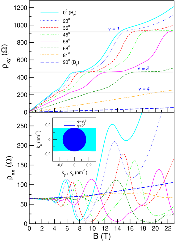
Experimental curves for a set of tilt angles collected on the sample A are displayed in Fig. 1.
 |
|
From the occurence of the quantum Hall effect we may conclude that the SL A represents a nearly perfect 2D system with negligible coupling of the 2D electron layers confined in the QWs. From the positions of the quantum Hall electron plateaux (, where are integer numbers and is the amount of QWs in the SL) we estimated that 28 QWs are occupied by electrons, which is very close to the nominal value 29. The electron concentration per layer cm-2 extracted from the linear part of the Hall magnetoresistance is in a good agreement with the value cm-2 obtained from the period of SdH oscillations at . Corresponding electron mobility per layer is cm2/Vsec. Oscillations of are shifted to higher fields with tilting the angle, satisfying the cosine law.
The FS of the sample A has a form of a smoothly corrugated (almost flat) cylinder (see the inset in Fig. 1) that was expected for the slightly coupled SL. It is difficult to detect the positions of “belly” (at the center of the Brillouin zone, ) and “neck” (at the Brillouin zone boundry, ) extremal cross-sections of the FS, as their areas are nearly the same.
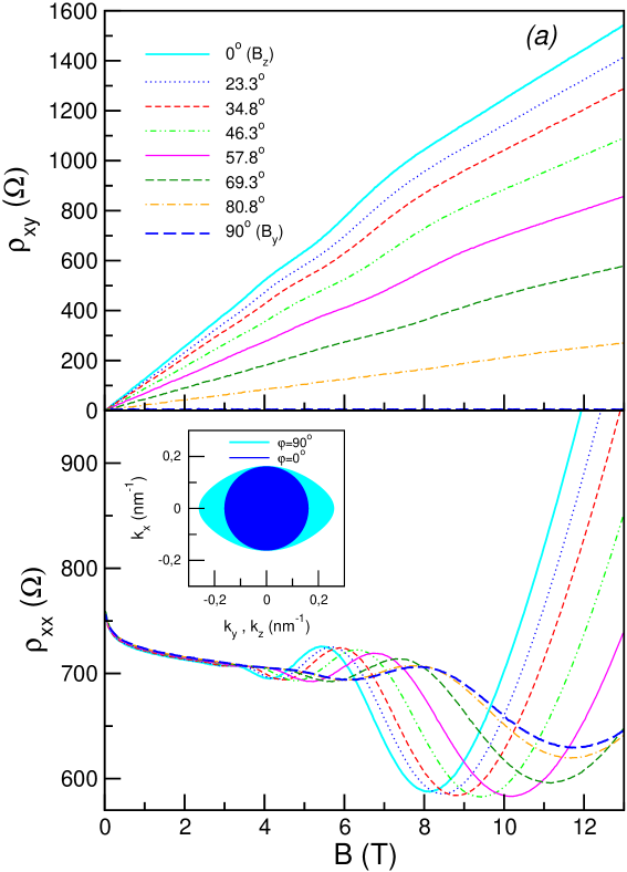
Magnetotransport data measured on the sample B before and after illumination are presented in Fig. 2. Magnetoresistance curves of the SL “in dark” exhibit strong deviations from the 2D behavior seen in the sample A. The Hall resistance grows almost linearly with increasing field. SdH oscillations can be seen for all slopes of the magnetic field even in the strictly in-plane orientation. These oscillations are found to be periodic in 1/B with a single period. Thus, the FS of the SL B “in dark” is formed by an ellipsoid [see the inset in Fig. 2 (a)] that confirms the 3D nature of the strongly coupled SL sample.
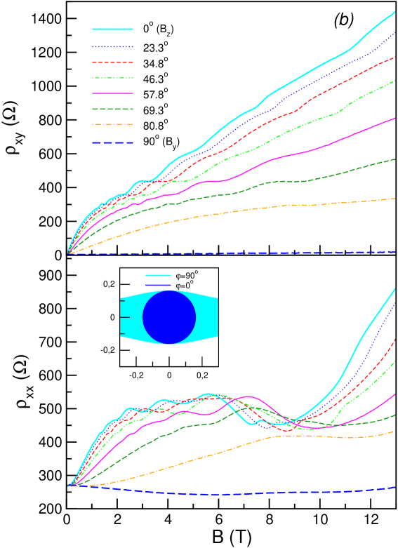
Illumination of the sample B dramatically changed the magnetoresistance curves. Hall plateaux appeared on curves. Oscillations of acquired more complicated forms and exhibit two distinct periods originated from “belly” and “neck” orbits. Oscillations weaken with increasing and disappear completely at . It means that the SL dimensionality has been reduced after illumination. The FS constructed from experimental periods of “belly” and “neck” SdH oscillations is another evidence. After illumination the FS of the SL B has changed its shape to a corrugated cylinder [see the inset in Fig. 2 (b)] characteristic for a system composed of weakly-coupled 2D electron layers.
As expected, the carrier concentration per layer was enhanced after illumination from the value cm-2 to cm-2. The electron mobility per layer increased significantly from cm2/Vsec to cm2/Vsec. Interpretation of the data in terms of the theory [4] simultaneously leads to a conclusion, that the ground SL miniband shrinks after illumination and therefore the inter-well coupling becomes weaker. Such a surprising behavior may be due to the presence of the metastable ionized deep donors within the barriers, which effectively increases their heights.
Acknowledgements
This work has been supported by the European Commission contract No. RITA-CT-2003-505474, Ministry of Education of the Czech Republic Center for Fundamental Research LC510 and Academy of Sciences of the Czech Republic project KAN400100652.
References
- [1] L. Esaki, R. Tsu, IBM J. Res. Develop. 14, 61 (1970).
- [2] L. Onsager, Phil. Mag. 43, 1006 (1952).
- [3] O. Jaschinski et al., Physica B 249-251, 873 (1998).
- [4] N. A. Goncharuk et al., Phys. Rev. B 71, 195318 (2005).