sss
Intrinsic spin-Hall accumulation in honeycomb lattices: Band structure effect
Abstract
Local spin and charge densities on a two-dimensional honeycomb lattice are calculated by the Landauer-Keldysh formalism (LKF). Through the empirical tight-binding method, we show how the realistic band structure can be brought into the LKF. Taking the Bi(111) surface, on which strong surface states and Rashba spin-orbit coupling are present [Phys. Rev. Lett. 93, 046403 (2004)], as a numeric example, we show typical intrinsic spin-Hall accumulation (ISHA) patterns thereon. The Fermi-energy-dependence of the spin and charge transport in two-terminal nanostructure samples is subsequently analyzed. By changing , we show that the ISHA pattern is nearly isotropic (free-electron-like) only when is close to the band bottom, and is sensitive/insensitive to for the low/high bias regime with such . With far from the band bottom, band structure effects thus enter the ISHA patterns and the transport direction becomes significant.
pacs:
73.23.-b, 72.25.-b, 71.70.EjIn electron systems, the extrinsic spin-Hall effect (SHE), theoretically proposed long time ago,DPspinHall ; Hirsch has been experimentally proven optically in semiconductor bulk structuresAwschalom science and two-dimensional electron systems (2DESs),Awschalom 2DEG and even electrically in diffusive metallic conductors.ElectricSpinHallExp Recent achievement on observing the SHE in 2DESs at room temperaturesRTspinHall has further enlightened the possibility to manipulate spins via the SHE based on such a simple mechanism: transverse spin separation by passing through longitudinal electric currents.
As for the intrinsic SHE, theoretically proposed much later than the extrinsic one,Sinova experimental evidence for its existence has been achieved only in two-dimensional hole systemsWunderlich but not in 2DESs. In particular, the local spin scanning in real-space for intrinsic SHE systems is difficult to carry out due to its limited size, and hence the required extra high resolution. Contrary to the extrinsic type, the intrinsic spin-Hall accumulation (SHA) pattern shows not only the out-of-plane component of spin accumulating antisymmetrically at the two lateral sides near the sample edges, but also oscillations due to the wave function modulation. Moreover, the SHA pattern may vary with, e.g., bias strength, spin-orbit coupling (SOC) strength, sample size and shape.Nikolic ; Shenger
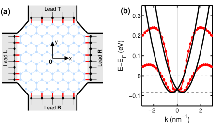
In this paper we further investigate the crystal-structure-dependence, and hence the band structure effect, of the intrinsic SHA (ISHA) pattern in 2DESs. The honeycomb lattice structure is particularly suitable for such investigation due to its nontrivial band structure and interesting geometry. In addition, recent confirmation of the strong Rashba SOCRashba on Bi surfaces,Hofmann review in particular the (111) case,Koroteev 2004 in which the projected bilayer structure exactly forms the honeycomb lattice, provides a good numerical example to demonstrate these effects. Based on the Landauer-Keldysh formalism (LKF),Nikolic the local spin densities (LSD) on four-terminal nanostructure samples made of the honeycomb lattice [see Fig. 1(a)], are calculated. We will show that the ISHA pattern (i) exhibits isotropic/anisotropic spin transport behaviors when the Fermi level is near/away from the band bottom, (ii) shows dramatic difference between the left-right (zigzag) and the bottom-top (armchair) transport modes when the Fermi level lies in the band gap, and (iii) is extremely sensitive to the Fermi level in the low-bias regime.
To apply the LKF, the first step is to construct the real space tight-binding-like Hamiltonian, which builds the underlying band structure and therefore is decisive for the transport properties. For the honeycomb lattice and considering both kinetic and Rashba hoppings up to the nearest neighbor only, the model Hamiltonian can be written asKane-Mele
| (1) |
with () being the creation (annihilation) operator of the electron on site . Here the first term is the on-site energy with parameter which may also describe the local potential and the disorder. In our potential-free case here, simply corresponds to the band energy offset in the language of tight-binding model (TBM). The second term in Eq. (1) contains the kinetic and Rashba hoppings with strengths and , respectively. In the Rashba hopping term, is the unit vector pointing from site to site , and is the Pauli matrix vector.
To obtain realistic values for the above parameters and we next perform the empirical TBMGrossoBook of the Slater-Koster type,Slater-Koster based on Eq. (1). Considering the two triangular sublattices forming the honeycomb lattice and taking only single orbital on each site into account, it can be shown that the Hamiltonian matrix equivalent to Eq. (1) reads
| (2) |
with the diagonal element given by where and are the -orbital energy and the identity matrix, respectively, and the off-diagonal element given by
| (3) |
where is the two-center interaction integral involving atomic orbitals, and the compact functions are given by and Note that for an ideal (flat) two-dimensional honeycomb lattice such as graphene, only the bands contribute to due to the vanishing direction cosine . However, later we will choose the Bi(111) bilayer structure as a numerical example, in which both and bands contribute due to the nonvanishing . Still, here in both cases only the composite parameter is to be extracted, instead of the individual and . Except the Rashba hopping strength which we denoted consistently in both Eq. (1) and the empirical TBM Eqs. (2) and (3), the other two parameters are related by and Diagonalizing the matrix of Eq. (2) gives the two pairs of the four energy dispersion curves.
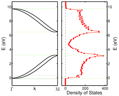
To extract reasonable parameters for Eq. (1), we consider the Bi(111) bilayer structure, for its strong surface states,Hofmann review making the electron transport 2DES-like, and its strong Rashba SOC,Koroteev 2004 making the ISHE thereon promising. Considering nearest-neighbor hopping only (and hence neglecting the interbilayer hopping), the projected two-dimensional lattice structure is exactly of honeycomb type. We therefore fit the energy dispersion curves obtained from diagonalizing Eq. (2) with the surface band structure from the first principle calculation,Koroteev 2004 as shown in Fig. 1(b). Both directions in this plot are along . Due to the simple model we have taken, the fitting gives good agreement only near the point. Correspondingly, the band parameters extracted from such fitting are and
The lead-sample setup is sketched in Fig. 1(a), where the sample made of the honeycomb lattice is of nearly square shape with four terminals (left, right, bottom, and top), each of which can be contacted by a semi-infinite normal metal lead. Throughout the rest of the calculations, we will set the and axes along the zigzag and armchair directions, respectively, and fix the origin of at the center of the sample, as indicated in Fig. 1(a).
The LKF, namely, the nonequilibrium Keldysh Green’s function formalismKeldysh applied on the Landauer multiterminal setups, has been summarized in some detail in Ref. Nikolic, . Its central spirit is to solve the kinetic equation for the Keldysh Green’s function matrix , written in the real-space representation at energy . Physical quantities such as local charge density (LCD), LSD, or even the charge and spin current densities, can then be extracted from . In systems free of phase-breaking interactions (such as electron-electron or electron-phonon interactions), the self-energy modifying the carrier life time inside the sample is contributed only from the contact leads through the nearest neighbor hopping with strength set equal to [see the bold (red) connection lines in Fig. 1(a)], and the Keldysh Green’s function can be solved exactly.DattaBook Explicitly, the self-energy can be expressed as the product of and the retarded surface Green’s function of the attached semi-infinite leads.Shenger ; DattaBook In our analysis, we will concentrate on -component of the LSD given byNikolic
| (4) |
where is the component spin operator with and is the position vector of the th lattice site. In the right-hand side, the matrix is the th diagonal submatrix element of the whole , is the Fermi energy to be tuned in the later analyses, is the electron charge, and is the applied potential difference between the negatively and positively biased leads. The LCD, which will be shown to modulate the LSD in the later analysis, is given by
| (5) |
where is the electron number operator. Note that here the band bottom , which is set to the lowest energy of the full band structure calculated from the previously introduced TBM, does not explicitly enter the expressions (4) and (5) but will play a decisive role in dealing with the self-energy due to the lead coupling. It may become even more crucial when calculating physical quantities to which equilibrium states also contribute, such as the bond spin current density.Nikolic
Before performing the LSD and LCD calculations, one last step is to report the convincing correspondence between the band structure of the infinitely extending honeycomb lattice, calculated by the empirical TBM, and the total density of states (DOS) of the finite-size sample, calculated by the LKF. The latter is given by summing the spectral function for each site where is the spin-resolved th diagonal submatrix element of the retarded Green’s function matrix. As shown in Fig. 2, the main features, including the band top, band gap, and band bottom, are nicely correspondent with each other. Note that the drop of the total DOS at the band gap region cannot be perfectly step-function-like since the sample considered in the LKF is not infinitely large.
Having constructed the correspondence between the empirical TBM and the LKF, and extracted reasonable parameters by fitting to the first principles calculation for the Bi(111) surface, we are now ready to present the local spin, and later also charge, densities on the conducting sample in the honeycomb lattice. Two bias regimes will be distinguished: low and high, standing for bias voltages of and , respectively, in the rest of the paper. Although there are totally four terminals free to contact the electrodes, we will consider only two-lead cases with head-to-tail orientation, either parallel to the or axes.
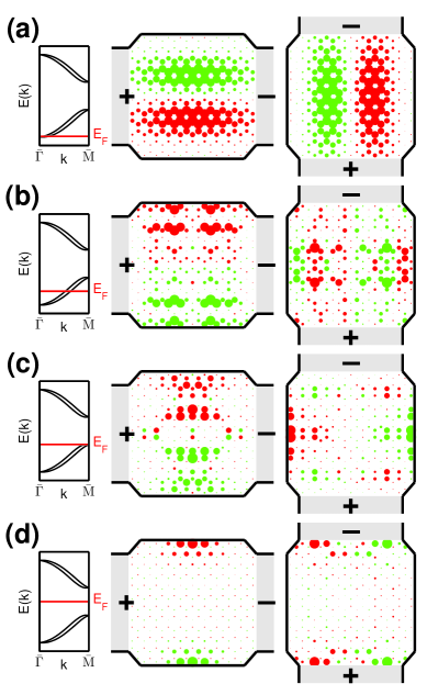
We first present the LSD for a sample of totally lattice sites (sample area about ) in the low bias regime. To examine the direction dependence of the spin transport, we set at some representative positions. As shown in Fig. 3, we gradually raise from the band bottom (, i.e., about above the bottom of the band, consistent with the first principle calculation) to the middle of the band gap (about ). In each panel of Fig. 3, the distribution is antisymmetric about the bias axis, and therefore exhibits the main feature of the intrinsic SHE. Furthermore, as can be clearly seen that, only when is set at the band bottom [Fig. 3(a)], the pattern becomes nearly isotropic, i.e., the spin transport does not show direction dependence and thus behaves as free electrons. With the increase of , Figs. 3(b) and 3(c) show distinct LSD distributions for the two different transport modes. Interestingly, when is set in the middle of the gap [Fig. 3(d)], a dramatic difference between the two transport modes emerges. In the left-to-right case spin accumulation occurs at the lateral edges, while in the bottom-to-top case there is almost nothing at the lateral edges but some spots induced near the leads. This can be understood by observing that at this Fermi energy the transport inside the sample is supported by the edge states, which are contributed mostly from the zigzag edges. Thus in the bottom-to-top geometry the whole sample behaves nearly insulating: neither charge nor spin can pass through the sample.
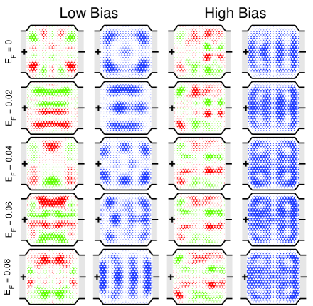
Next we take further looks at the spin and charge transport near . We consider a sample with 802 sites (about ) with two leads in the left-to-right orientation, and finely raise the Fermi level from to . Both the low and high bias regimes will be analyzed. As shown in the first column of Fig. 4, the ISHA pattern in the low-bias regime is extremely sensitive to the Fermi level. Compared to the LCD in the second column of Fig. 4, one can see that such sensitivity stems from the wave function modulation. Whereas the nonequilibrium transport is contributed from the states between and , the low bias regime with small voltages is mainly described by the Fermi energy state, and the electron transport thus behaves quantum mechanically. It turns out that the Fermi level, determining the length of the wave vector , influences the formation of the electron wave, and hence in turn the ISHA pattern. It is interesting to note that a strong accumulation of electrons does not necessarily lead to a prominent accumulation of spins. Conversely, where there are no electrons, there must be no spins. Put in another way, the local spin and charge density patterns must be, to some extent, consistent with each other.
For the high bias case, both the local spin and charge densities change moderately with the increase of (the two right columns in Fig. 4). Contrary to the low bias regime, the involved states participating electron transport cover a much wider range of energy. Summation of these states with different wave lengths eventually gives a waveless charge distribution, as compared to the low-biased patterns. The electron transport behavior is therefore far from the standard quantum-mechanical description. In this case the nonequilibrium spin accumulation is no longer affected by the wave function modulation, and the ISHA pattern is robust against the change of .
Before closing, it is worthy to remark here that in the pioneering formulation of Ref. Nikolic, , and also the recent application of Ref. Shenger, on the triangular lattices, the crystal structure information is lost since the Fermi energy is chosen close to the band bottom: . Consequently, the spin accumulation property remains free-electron-like and exhibits rotational invariance (except for a coexistence of the Dresselhaus term, giving rise to anisotropic dispersion). It is only when the Fermi level is far from the band bottom, where the corresponding wave vectors are short, that the band structure (or the crystal structure) effect emerges.
In conclusion, taking the honeycomb lattice as a particular case, we have pointed out the crucial role plays in the ISHE due to band structure effects. Recent observation of the strong surface state and giant Rashba SOC on Bi(111) surfaceKoroteev 2004 has attracted much attention and is especially suitable as a numeric example in our investigation. The possibility of observing the quantum SHE on the Bi(111) surface and its multilayer thin filmMurakamiBi has made Bi(111) even more promising. Here we have reported another positive viewpoint of its potential of observing the ISHE thereon, provided that and the transport direction are important. Moreover, we have combined the LKF with the first principle band calculation through the empirical TBM, allowing one to extract realistic band parameters for the LSD calculation.
One of us (M.H.L.) appreciates the hospitality in Forschungszentrum Jülich, where most of this work was performed. Financial support of the Republic of China National Science Council Grant No. 95-2112-M-002-044-MY3 is gratefully acknowledged.
References
- (1) M. I. Dyakonov and V. I. Perel, JETP Lett. 13. 467 (1971); M. I. Dyakonov and V. I. Perel, Phys. Lett. A 35, 459 (1971).
- (2) J. E. Hirsch, Phys. Rev. Lett. 83, 1834 (1999).
- (3) Y. K. Kato, R. C. Myers, A. C. Gossard, and D. D. Awschalom, Science 306, 1910 (2004).
- (4) V. Sih, R. C. Myers, Y. K. Kato, W. H. Lau, A. C. Gossard, and D. D. Awschalom, Nat. Phys. 1, 31 (2005).
- (5) S. O. Valenzuela and M. Tinkham, Nature (London) 442, 176 (2006).
- (6) N. P. Stern, S. Ghosh, G. Xiang, M. Zhu, N. Samarth, and D. D. Awschalom, Phys. Rev. Lett. 97, 126603 (2006).
- (7) Jairo Sinova, Dimitrie Culcer, Q. Niu, N. A. Sinitsyn, T. Jungwirth, and A. H. MacDonald, Phys. Rev. Lett. 92, 126603 (2004).
- (8) J. Wunderlich, B. Kaestner, J. Sinova, and T. Jungwirth, Phys. Rev. Lett. 94, 047204 (2005).
- (9) Branislav K. Nikolić, Satofumi Souma, Liviu P. Zârbo, and Jairo Sinova, Phys. Rev. Lett. 95, 046601 (2005); Branislav K. Nikolić, Liviu P. Zârbo, and Satofumi Souma, Phys. Rev. B 73, 075303 (2006).
- (10) Son-Hsien Chen, Ming-Hao Liu, and Ching-Ray Chang, Phys. Rev. B 76, 075322 (2007).
- (11) Y. A. Bychkov and E. I. Rashba, J. Phys. C 17, 6039 (1984).
- (12) Ph. Hofmann, Prog. Surf. Sci. 81, 191 (2006), and references therein.
- (13) Yu.M. Koroteev, G. Bihlmayer, J. E. Gayone, E.V. Chulkov, S. Blügel, P.M. Echenique, and Ph. Hofmann, Phys. Rev. Lett. 93, 046403 (2004).
- (14) C. L. Kane and E. J. Mele, Phys. Rev. Lett. 95, 146802 (2005).
- (15) Giuseppe Grosso and Giuseppe Pastori Parravicini, Solid State Physics (Academic Press, New York, 2000).
- (16) J. C. Slater and G. F. Koster, Phys. Rev. 94, 1498 (1954).
- (17) L. V. Keldysh, Sov. Phys. JETP 20, 1018 (1965).
- (18) Supriyo Datta, Electronic Transport in Mesoscopic Systems (Cambridge University Press, Cambridge, 1995).
- (19) S. Murakami, Phys. Rev. Lett. 97, 236805 (2006).