Screening effects on field emission from arrays of (5,5) carbon nanotubes: Quantum-mechanical simulation
Abstract
The simulation of field electron emission from arrays of micrometer-long open-ended (5, 5) carbon nanotubes is performed in the framework of quantum theory of many electrons. It is found that the applied external field is strongly screened when the spacing distance is shorter than the length of the carbon nanotubes. The optimal spacing distance is two to three times of the nanotube length, slightly depending on the applied external fields. The electric screening can be described by a factor that is a exponential function of the ratio of the spacing distance to the length of the carbon nanotubes. For a given length, the field enhancement factor decreases sharply as the screening factor larger than 0.05. The simulation implies that the thickness of the array should be larger than a value but it does not help the emission much by increasing the thickness a great deal.
pacs:
73.22.-f 73.21.-b 79.70.+qI Introduction
For the application of carbon nanotubes (CNTs) as the cold cathodes of field electron emission (FE), the ideal structure is to arrange the CNTs into an aligned array. It has been observed that the spacing distance of CNTs affects FE properties remarkably.a1 ; a2 ; a3 ; a4 ; a5 ; a6 ; a7 ; a8 ; a9 It is clear that denser and longer CNT bundle has stronger screening effect that would reduce the field electron emission of each CNT. On the other hand, larger spacing distance decreases the number of CNTs in a unit area, which leads to weaker mean emission current density. It is important to describe the screening quantitatively and to find out its effect on the FE ability. The calculation of Nilsson et al.a1 suggested that the optimum spacing distance would be twice the length of the CNTs. However, Jung Sang Suh et al.a2 showed that the emission current density is optimized when the length of the CNTs is equal to the spacing distance. By solving Laplace’s equation, Bocharov and Eletskiia9 found that the emission current density has the maximum value when the spacing distance is half of the length of the CNTs. More careful studies on this topic would obviously be useful. In this paper, we will simulate the FE of the array of single-walled carbon nanotubes (SWCNTs) with a quantum/molecular hybrid method.
Under the applied external field (denoted by ), it has been known that the SWCNT is charged.a10 Therefore, the SWCNTs of the array are coupled to each other through the Coulomb interaction. The excess charges are also the origin of the screening. The competition between the screening effect and the density of CNTs would be complicated by the field enhancement factor that is length-dependent. The field enhancement factor was presumably proportional to the aspect ratio of the SWCNT. However, recent quantum simulations revealed that the field penetration at the apex of the SWCNT is significant.a10 ; a11 The field penetration depends on the value of the applied external field, thereby it is also related to the screening effect. The enhancement factor of the array has been calculated by the classical method.a9 When the charge redistribution and the screening effect are taken into account, as will be shown in the present paper, the field enhancement factor of the array is different from the classical one obviously.
To estimate the excess charge distribution and the field penetration at the apexes of SWCNT arrays, it requires a large-scale simulation that should reflect both the quantum electron structure at the apex and the Coulomb interaction over the tubes. In experiments, the length of CNTs is usually in micrometers, while the radius is in nanometers. A huge number of freedoms are involved. For instance, the (5, 5) type SWCNT of 1 m length consists of about carbon atoms. Limited by the computational efficiency and resources, all ab initio studies so far can only simulate the local properties involving hundreds of carbon atoms. As the electronic properties are sensitive to both the detailed atomic arrangement (i.e., the location of defects, adsorbates, and the chirality) and the distribution of excess charges over the whole tube, it is a big challenge to simulate a SWCNT array that consists of SWCNTs with length in the order of micrometer. Only recently has it been possible to tackle an individual SWCNT of realistic size in the FE conditions by a multiscale method involving quantum mechanics and molecular mechanics.a10 ; a11 In the present paper, we adopted this method to simulate the FE of the SWCNT array, of which the length is in the micrometer scale. The structure of the SWCNTs is specified to the (5, 5) armchair type. The dangling bonds in the open mouths of the SWCNTs are saturated by hydrogen atoms. We further assume that the SWCNTs are vertically mounted on a metal surfaced uniformly. Therefore only one SWCNT is required to be dealt with in the environment of other SWCNTs. Each SWCNT of the array is treated as a replica of the SWCNT under simulation.
In Section II, the simulation method is reviewed briefly. The simulation results are presented and discussed in Section III. The dependence of the screening on the spacing distance, the length, and the applied external fields are discussed in Section IV, where a factor is introduced to describe the screening, and the correlation between this factor and the field enhancement factor is presented. The last section gives the conclusions.
II Simulation Method
The CNT array for FE is a typical multiscale system. In our model, the CNT array is under the uniform applied external field, whose direction is parallel to the axes of the CNTs, and the SWCNTs are mounted vertically and formed a regular square lattice on the cathode surface. The distance of two nearest neighbored SWCNTs (to be referred to as ”spacing distance”) and the length of SWCNTs in the array are denoted by d and L, respectively. When a field is applied to the SWCNT array, the electrons have opportunity to emit into vacuum through the apexes of the SWCNTs by quantum tunneling.
Since electrons are emitted from the apex of each SWCNT by quantum tunneling, the apex part must be treated by quantum mechanics. The part on the substrate side mainly affects the field emission through Coulomb potential of the excess charges, so it can be treated by a semiclassical method.a10 ; a11 Therefore we should divide each SWCNT into a quantum region and a semiclassical region. The quantum region is dealt with on atomic scale where the density matrix of the electrons is obtained quantum mechanically. The quantum region should be large enough to ensure that the artificial division does not affect the physical results seriously. By our experience, the proper size of the quantum region is much bigger than that the standard ab initio methods could deal with. We have to further divide the quantum region into sub-regions. Each sub-region together with its adjacent sub-regions forms a subsystem that is dealt with by the modified neglect of diatomic overlap (MNDO)Dewar semiempirical quantum mechanical method (here the MOPAC software has been used). The excess charges outside the subsystem being dealt with are treated as point charges. Their contribution to the subsystem being dealt with is through the Coulomb interaction. To accelerate the simulation, we first simulate an isolated subsystem under various external fields. Assuming all subsystems except that contains the apex are resemble to the isolated subsystem, their electron density can be read out from the database, which has been constructed by simulating the isolated subsystem, with the entry of electric field that is the superposition of the applied external field and the fields contributed by the excess charges in other parts of the array as well as by the image charges. With this acceleration algorithm, we are able to deal with a quantum region of length over 900 nm.
Although in principle we can deal with an entire isolated SWCNT quantum mechanically, the connection of the SWCNT and the cathode is too complicate for a full quantum treatment. It is convenient to treat the part of SWCNT connecting the cathode as the semiclassical region. In the semiclassical region, the Coulomb potential is governed by Poisson’s equation. The boundary condition of the metal surface is guaranteed by the image charges of the excess charges of the SWCNTs. It should be noted that even in the semiclassical region the electron energy band structure originating from the quantum mechanics should be taken into account. For the (5, 5) SWCNT, there are both experimental and theoretical evidences for the constant density of state (DOS) in the vicinity of the neutrality level.a12 ; a13 ; a14 ; a15 It turns out that the excess charge density can be approximated by a linear function of the longitudinal coordinate of the SWCNT.a16
The coupling of quantum region and semiclassical region is through the quasithermodynamic equilibrium condition which assumes that the chemical potential (Fermi level) is a constant over the entire array. To avoid the complexity arose from the Schottky junction that would emerge at the back contact in principle, we simply assume the Fermi level of the SWCNTs is 5.0 eV below the vacuum potential in the absence of applied external field. The density of the excess charge (”excess density” for simplicity) calculated separately in quantum and semiclassical regions should coincide at an overlap place of two regions. The self-consistent excess density of the entire SWCNT array is achieved through iterations that contain a small loop and a big loop. In the small loop, the subregions of the quantum region are dealt with one by one, and repeated until that a converged electron density in the quantum region is obtained. In the big loop, the quantum region and the semiclassical region are dealt with alternatively until the self-consistent charge distribution is achieved.
III Simulation Results
It has been shown that the vacuum potential barrier in the circumambience of the SWCNT is high and thicka10 , therefore the electrons would most probably emit forward from the first layer of the tip. The transmission coefficient (D) can be estimated by the WKB approximation
| (1) |
where U(z) is the electron energy potential, is the Fermi energy, and the integral is over the classical forbidden region where . We have assumed that the electrons possess the Fermi energy.
With D in hand, the emission current of each SWCNT is estimated by
| (2) |
where are the extra electrons of the first layer atoms, and is the collision frequency (the number of electrons hitting the barrier per unit time) that can be estimated from the average kinetic energy of electrons as , which is approximately equal to Hz.
We should focus at the electrostatic potential U(z) in the vicinity of the apex of the SWCNT, which determines the major feature of the FE of the array.
III.1 Varying spacing distance
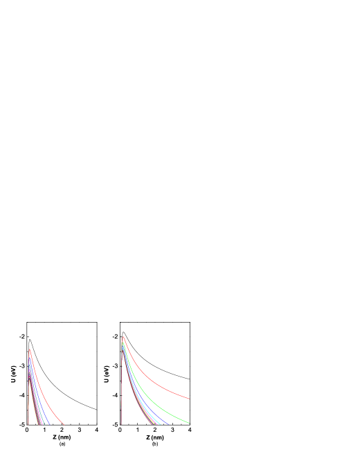
In Fig. 1(a)/(b), we plot U(z) of different spacing distances under the applied external field, =12.0 V/m. The length of the tubes, i.e., the thickness of the array, is 1.00 m in Fig. 1(a) and 0.75 m in Fig. 1(b). The Z axis has its origin at the last atom of the SWCNT and is parallel to the direction of the tube axis. The Fermi level of the electrons in the nanotubes is assumed to be -5.0 eV in our simulation. Therefore the potential profiles shown in Fig. 1 are in fact the apex-vacuum potential barriers that control the probability of electron tunneling. The observation of the barrier height lowering as d increasing is consistent with the FE mechanism of field-reduced barriera10 since larger d should lead to smaller field screening and increase the effective field applying to the SWCNTs. The sharper shape of Fig. 1(a) comparing with Fig. 1(b) is a consequence of the field enhancement. The curves almost coincide with each other for d1.5 m in Fig. 1(a)/(b), implying that the screening effect is negligible when d1.5 m.
The mean current density from the array (”current density” for simplicity and denoted by J) against d are presented in Fig. 2 for three sets of parameters. The lengths of SWCNTs are 0.75 m, 1.00 m, and 1.00 m; the external fields are 12.0 V/m, 12.0 V/m, and 10.0 V/m for the Figs. 2(a), (b), and (c), respectively. The current density is very sensitive to both L and (the J axes for Figs. 2(a), (b), and (c) are multiplied by the factors , , and , respectively). It is notable that the emission is turned-on at certain spacing distance, which is about 1.0 m here, roughly equal to the length of the tube. Comparing Figs. 2(a) , (b), and (c), one may see that both the turn-on spacing distance and the maximum of J would depend on .


The parabolic decrease of the current density as the spacing distance getting large can be easily understood by the fact that the current density is proportional to the number of SWCNTs in a unit of area when the screening effect is negligible.
III.2 Varying length
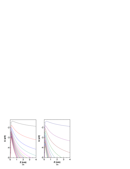
We plot the U(z) for different L under the applied external field =10.0 V/m, with d=0.75 in Fig. 3(a) and 1.00 m in Fig. 3(b). The lowering of apex-vacuum barrier is associated with the excess charge accumulation at the apex. For the same L, the barrier of larger d is lower than that of shorter d. It implies that the array of larger d can accommodate more excess charges at each apex.
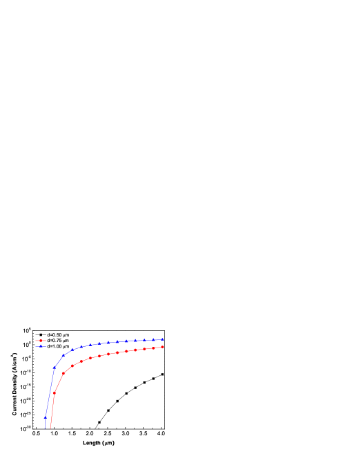
The current density as a function of L is shown in Fig. 4. The squares, circles, and triangles in this figure are corresponding to the data of d=0.50 m, d=0.75 m, and d=1.00 m, respectively. From this figure, one sees that the emission current densities of the array of short SWCNTs are negligible. The minimum length for a significant current density (say A/) is enlarged as the spacing distance decreases. The rapid increase of the current densities is the consequence of the field enhancement. However, when L is large, the screening has significant effects and the current densities only increase moderately. The array with L=0.5 m can hardly emit electrons.
III.3 Varying applied external field
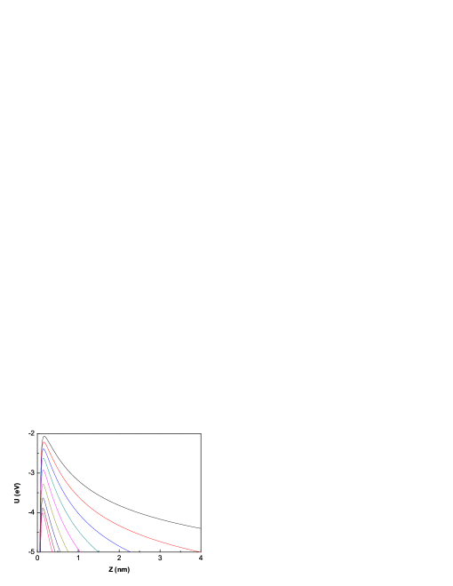
We have considered the array with d=2.00 m and L=1.00 m for various applied external fields. The electron potential U(z) is presented in Fig. 5 for ranged from 7 to 15 V/m.
The J- characteristic is given in Fig. 6. The inset of Fig. 6 is the Fowler-Nordheim plot. The nonlinear Fowler-Nordheim plot implies that the mechanism for the FE of the SWCNT array could be different from that of the metal plane emitters.

IV Screening Factor
In order to describe the screening effect quantitatively, we define a screening factor as
| (3) |
where V is the voltage drop (related to the substrate) at the middle point of the line connecting two neighborhood apexes. It should be zero if there is no screening and equal to 1 if the array, as an ideal metal layer of thickness L, screens the field completely. The screening factor versus d/L is shown in Fig. 7(a) for four sets of parameters: (1) d=0.75 m, =12.0 V/m; (2) d=1.00 m, =12.0 V/m; (3) L=0.75 m, =10.0 V/m; (4) L=1.00 m, =10.0 V/m. The upper (lower) triangles are corresponding to various d with fixed L=0.75 (1.00) m. The squares (circles) are corresponding to various L with fixed d=0.75 (1.00) m. Notably, all points fall into a curve, implying that the screening factor is a function of d/L. The best fitting to the simulation (solid curve) is
| (4) |
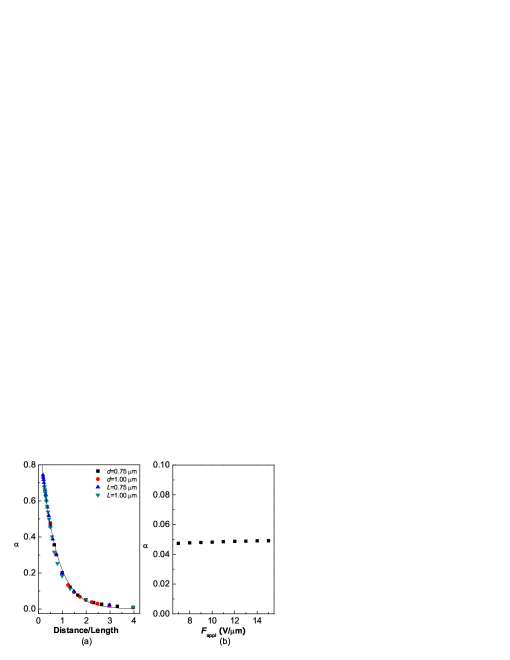
For the array of d=2.00 m and L=1.00 m, the screening factor is calculated with different . As shown in Fig. 7(b), we find that it is almost independent of the applied external field. It implies that the screening factor fixed by the ratio d/L is an intrinsic feature of the array.
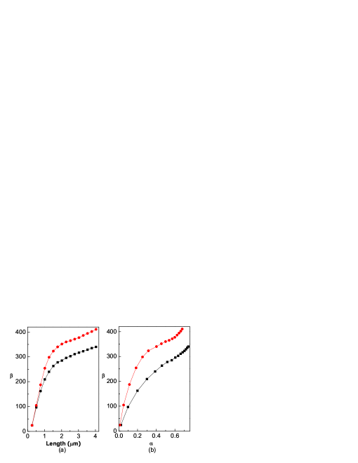
From the data of U(z), we can estimated the local field strength () as the value of the slope of the barrier potential U(z) at the point of steepest decrease. An effective field enhancement factor can then be defined as /. Figure 8 shows the correlation between and the tube length (a), and the correlation between and the screening factor (b), for fixed and d . The field enhancement factor of the array is not proportional to the tube length, which is completely different from an individual nanotube (or a metal tip). The increase of tube length strengthens and the screening tends to reduce . But the increase L will lead to increase of screening. Therefore, the dependence of on L and is complicate. If there were no screening, in Fig. 8(b) should increase faster.
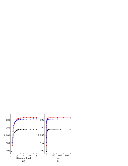
The reduction of field enhancement by screening can be seen more clearly in Fig. 9 for a few sets of applied external fields and tube lengths. Figure 9(a) shows that for large spacing distance, where the screening is week, the field enhancement factor tends to a constant. For a given L, the classical field enhancement factor should be a constant. However, as one seen in 9(b), that would be true only if the screening could be ignored. For the instances of the 9(b), the field enhancement factor decreases sharply as increase when .
V Conclusions
We have studied the field electron emission properties of arrays of
single-walled carbon nanotubes in the quantum level. As the spacing distance of
the SWCNTs exceeds a certain value (about the length of the tube), the emission
current density increases rapidly. When the spacing distance is large enough,
the current density decreases with the spacing distance as a parabolic
function. An optimal spacing distance that corresponds to the maximum current
density could be two to three times of the nanotube length. The exact value of
the ratio corresponding to the peak current density would depend on the applied
external field and the tube structure. That would be one of the reasons for the
discrepancy of experimental results of different groups. The screening effect
can be described by the factor () defined in Eq. 3, which is
found to be an exponential decreasing function of the ratio of the spacing
distance to the length of the SWCNTs, and is almost independent of the applied
external field. Therefore, the screening factor introduced here reflects an
intrinsic character of the array. When , the screening effect can
be ignored and each SWCNT of the array behaves as an individual emitter. For
large , on the other hand, the emission property of a SWCNT in the
array is obviously different from the individual SWCNT. The field enhancement
factor of the SWCNT array is not a linear function of the tube lengths as the
metal rod model predicted. And it depends on the applied external fields and
the spacing distances. For a given tube length, it is a monotonically
decreasing function of the screening factor. Although the field enhancement
factors depends on the spacing distance (Fig. 4(a)) in the same trend
as the classical calculationa9 , the quantitative discrepancy between
quantum simulation and classical calculation is large. To increase the emission
current density, one can either adjust the spacing distance or increase the
lengths of the tubes. For the (5,5) SWCNT array considered in the present
paper, we find that the current density is very small for the spacing distance
0.5 m. For larger spacing distance (0.75 and 1.0m, for instances),
the current density increases rapidly as the length increases until the length
is as large as 1.5 times of the spacing distance. For longer length, the
current density only increases slowly. It implies that lengths of SWCNTs of the
arrays need not be too long.
Acknowledgement. The project is supported by the National Natural Science Foundation of China (Grant No. 10674182, 90103028, 90306016) and National Basic Research Program of China (973 program 2007CB935500).
References
- (1) L. Nilsson, O. Groening, C. Emmenegger, O. Kuettel, E. Schaller, L. Schlapbach, H. Kind, J-M. Bonard, and K. Kern, Appl. Phys. Lett. 76, 2071 (2000).
- (2) J. S. Suh, K. S. Jeong, J. S. Lee, and I. Han, Appl. Phys. Lett. 80, 2392 (2002).
- (3) S. H. Jo, Y. Tu, Z. P. Huang, D. L. Carnahan, D. Z. Wang, and Z. F. Ren, Appl. Phys. Lett. 82, 3520 (2003).
- (4) Y. M. Wong, W. P. Kang, J. L. Davidson, B. K. Choi, W. Hofmeister, and J.H. Huang, Diamond & Related Materials 14, 2078 (2005).
- (5) K. B. K. Teo, E. Minoux, L. Hudanski, F. Peauger, J-P. Schnell, L. Gangloff, P. Legagneux, D. Dieumegard, G. A. J. Amaratunga, and W. I. Milne, Nature 437, 968 (2005).
- (6) X. Q. Wang, M. Wang, H. L. Ge, Q. Chena, and Y. B. Xu, Physica E 30, 101 (2005).
- (7) X. Q. Wang, M. Wang, Z. H. Li, Y. B. Xu, and P. M. He, Ultramicroscopy 102, 181 (2005).
- (8) D. Nicolaescu, V. Filip, G. H. Takaoka, Y. Gotoh, and J. Ishikawa, J. Vac. Sci. Technol. B 25, 472 (2007).
- (9) G. S. Bocharov and A.V. Eletskii, Technical Physics 50, 944 (2005).
- (10) X. Zheng, G. H. Chen, Z. Li, S. Deng, and N. Xu, Phys. Rev. Lett. 92, 106803 (2004).
- (11) J. Peng, Z. Li, C. He, S. Deng, N. Xu, X. Zheng, and G. H. Chen, Phys. Rev. B 72, 235106 (2005).
- (12) M. J. S. Dewar and W. Thiel, J. Am. Chem. Soc, 99, 4899 (1977).
- (13) Rakwoo Chang, Gary S. Ayton, and Gregory A. Voth, J. Chem. Phys. 122, 244716 (2005).
- (14) A. M. Rao, E. Richter, S. Bandow, B. Chase, P. C. Eklund, K. A. Williams, S. Fang, K. R. Subbaswamy, M. Menon, A. Thess, R. E. Smalley, G. Dresselhaus, and M. S. Dresselhaus, Science 275, 187 (1997).
- (15) X. Blas, L. X. Benedict, E. L. Shirley, and S. G. Louie, Phys. Rev. Lett. 72, 1878 (1994).
- (16) R. A. Jishi, J. L. Bragin, and L. Lou, Phys. Rev. B 59, 9862 (1999).
- (17) Z. Li and W. Wang, Chin. Phys. Lett. 23, 1618 (2006).