Transport properties of chemically synthesized polypyrrole thin films
Abstract
The electronic transport in polypyrrole thin films synthesized chemically from the vapor phase is studied as a function of temperature as well as of electric and magnetic fields. We find distinct differences in comparison to the behavior of both polypyrrole films prepared by electrochemical growth as well as of the bulk films obtained from conventional chemical synthesis. For small electric fields , a transition from Efros-Shklovskii variable range hopping to Arrhenius activated transport is observed at . High electric fields induce short range hopping. The characteristic hopping distance is found to be proportional to . The magnetoresistance is independent of below a critical magnetic field, above which counteracts the magnetic field induced localization.
pacs:
71.23.Cq, 72.20.Ee, 73.20.HtI INTRODUCTION
Polypyrrole (PPy) is a semiconducting polymer with some unusual properties compared to other organic semiconductors Skotheim et al. (1998). The material can be synthesized both chemically and electrochemically; the electrosynthesis Yoon et al. (1994) can be performed at low polymerization potentials, allowing the use of water as solvent Asavapiriyanont et al. (1984); Rodriguez et al. (1997); Simonet and Berthelot (1991). Typically, such films have a rather large thickness above 1 micron, and they are highly disordered as well as crosslinked; maximum conductivities of 1600 S/cm have been reported for stretched films Yamamura et al. (1988). In addition, PPy can be doped electrochemically to a high level, which stabilizes the material properties under ambient conditions Kanazawa et al. (1980); Diaz et al. (1981); et al. (2005). A wide range of applications has been demonstrated, such as gas sensors Marcos and Wolfbeis (1997); Bidan (1992); Malinauskas (2001); Geng et al. (2006), biosensors Cosnier (2000), or transistors Chung et al. (2005); Lee et al. (2005); and Heinzel (2006).
The transport properties of electrochemically synthesized PPy films have been studied extensively Yoon et al. (1994); Skotheim et al. (1998). In the insulating state that is usually present, the samples typically follow the Efros-Shklovskii (ES) variable range hopping model Shklovskii and Efros (1988); Efros and Shklovskii (1975). Such a system is assumed to be formed by metallic sites separated by tunnel barriers Menon et al. (1998); Kohlman and Epstein (1998), which are
generated by spatial variations in the charge density. The electric field dependence of the conductivity was investigated by Ribo et al. Ribo et al. (1998). More recently, Gomis and co-workers Gomis et al. (2003) reported
an electric field - induced transition from an insulating to a metallic state which is reached when the electric field is strong enough to delocalize a small fraction () of the charges.
Chemical synthesis Joo et al. (2000), on the other hand, allows film preparation on conductive as well as on insulating substrates, thereby complementing the range of applications. Chemically grown films have a pronounced egg-like morphology
Zhang et al. (2006), markedly different than the characteristic fibers obtained by electrochemical synthesis. These films are, however, of notoriously poor quality in terms of roughness and conductivity. For example, their reported maximum room temperature conductivities are Chakrabarti et al. (2002); Winther-Jensen
et al. (2004). This may be the reason why only a very limited number of works have addressed the transport properties of this kind of PPy films. The existing studies have demonstrated that in films with thicknesses larger than , the temperature dependence of the conductance is consistent with three-dimensional Mott variable range hopping, i.e. Joo et al. (2000); Chakrabarti et al. (2002). Up to now, chemical synthesis of PPy at reduced temperatures has not been reported, which is somewhat surprising considering the profound influence the growth temperature has on the conductivity of electrochemically synthesized films Yoon et al. (1994).
Here, we present an investigation of the transport properties of PPy thin films and low roughness, prepared by a recently established scheme that allows the formation of thin films by chemical polymerization from the vapor phase and Heinzel (2006). The differential conductance is studied as a function of electric and magnetic fields as well as of temperature. With small electric fields applied, we find that for low temperatures, the electronic transport can be described within the ES-variable range hopping model. Above a temperature of , Arrhenius-type activated transport is found. As the electric field is increased, a transition to short-range hopping is observed around a characteristic electric field of . This electric field - induced reduction of the localization is also visible in magnetotransport measurements.
II SAMPLE PREPARATION AND CHARACTERIZATION
PPy films were synthesized via chemical polymerization from pyrrole vapor in solutions of . The preparation scheme follows that one described in detail in a previous publication and Heinzel (2006), except that our solvent was cooled, with a minimum growth temperature of . At lower temperatures, the polymerization kinetics became unacceptably slow. A thin PPy film was formed on a doped and oxidized Si substrate containing four Pt electrodes. The film thickness is proportional to the exposure time to the vapor and can be tuned between a few nanometers and . In the present study, we focus on films of thickness . We observe that besides growth at , also water created by decomposition of , an aging process in the solution, increases the contact resistance. Therefore, fresh solution has been used for each sample.
Films have been grown at temperatures between and in solutions with volume fractions varying between and . Cyclic voltammetry measurements et al. (2005) allow us to estimate the doping density of all samples to . This and the fact that the doping density depends neither on the growth temperature nor on the volume fraction of the solution indicates that the films are in the fully charged state, corresponding to 0.25 and 0.33 holes per pyrrole ring Bredas et al. (1983, 1984). The electronic transport has been studied in eleven samples, all showing qualitatively identical behavior. Typical room temperature conductivities of are found, with no apparent systematic dependence on or on the volume fraction of the solution. At temperatures below , however, samples grown at show substantially lower conductivities than samples grown below this temperature. In the following, we focus on three samples, the parameters of which are summarized in Table 1.
| Sample | volume | |||||
|---|---|---|---|---|---|---|
| [K] | fraction | [S/cm] | [nm] | [nm] | [nm] | |
| A | 282.0 | 1:1000 | 10 | 1.5 | 30 | 8 |
| B | 277.5 | 1:1000 | 12 | 3.4 | 44 | 12 |
| C | 277.5 | 4:1000 | 20 | 8.8 | 72 | 19 |
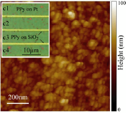
Figure 1 shows an atomic force microscope image of the surface of sample A and the corresponding
four-electrode device as seen in an optical microscope (inset), where the gap between the electrodes
is . The PPy film covers the 4 Pt electrodes (c1 to c4). The roughness (single standard deviation)
decreases with decreasing growth temperature, varying from 25% of the film thickness for the samples grown at to
6% for the samples grown at . The film morphology shows egg-like structures well known for chemically
synthesized PPy Zhang et al. (2006), with an average diameter of .
Transport measurements have been carried out in a gas flow cryostat with a temperature range between and . The cryostat is equipped with a superconducting magnet (maximum magnetic field ). Our setup has a DC current resolution of . By comparing two-probe with four probe measurements, we found negligible contact resistances for all experimental conditions investigated. Samples that were measured at temperatures above with applied electric fields got permanently damaged, while below , up to could be applied.
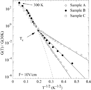
In Fig. 2, the temperature dependence of the conductance for the three samples under small electric fields () is shown. Below , behaves in accordance with the standard ES - variable range hopping relation Efros and Shklovskii (1975); Shklovskii and Efros (1988), given by
| (1) |
with
| (2) |
Here, denotes the localization length, and is the dielectric constant of PPy Van and Potje-Kamloth (2000); Koezuka and Etoh (1983). Below , the current vanishes in our noise floor. We have fitted to eq. 1 for temperatures below . For sample A, is obtained, corresponding to (see Table 1 for the corresponding results obtained for samples B and C). The characteristic hopping distance within the ES-variable range hopping model is given by
| (3) |
The values of at and are displayed in Table 1. At the critical temperature , shows a crossover from ES-variable range hopping to Arrhenius behavior, which is characterized by
| (4) |
Such a crossover is expected at a temperature where nearest neighbor hopping begins to dominate over variable range hopping Mott (1974). It has been observed in several other systems, for example in gold nanoparticle multilayers Tran et al. (2005), or in nanocrystal assemblies Roest et al. (2003).
For nearest neighbor hopping, the activation energy is given by Yu et al. (2004)
| (5) |
where denotes the nearest neighbor distance. From fits of eq.(4) to the data, the activation energy is found to be
for all samples. Via eq. 5,
this corresponds to .
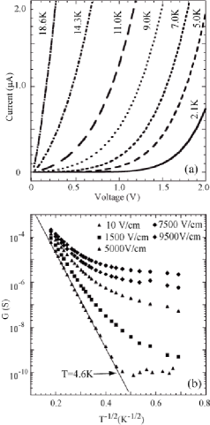
We proceed by discussing the effect of high electric fields. Fig. 3 (a) shows the IV traces as a function of the temperature for sample A. All samples exhibit a non-linear IV characteristics below . In Fig. 3 (b), the differential conductance is shown for sample A for various electric fields . Clearly, the electric field has a profund effect on the conductance; it can induce changes of over more than four orders of magnitude at low temperatures over the accessible electric filed range, and strong deviations from eq. (1) occur: the shape of becomes strongly dependent on , while the temperature dependence of decreases with increasing electric field. Our data can be interpreted within the extension of the ES - variable range hopping model to significant electric fields: it has been argued that for samples in the ES-variable range hopping regime, the electric field reduces the Coulomb energy over a characteristic hopping distance by Dvurechenskii et al. (1988), which for intermediate electric fields results in a modified conductivity given by
| (6) |
This intermediate regime is defined by , where and denote a lower and upper critical electric field, respectively. is a length parameter of the order of the maximum hopping length, the exact numerical value of which is under controversial discussion Hill (1971); Pollak and Riess (1976); Shklovskii (1976). In this intermediate regime, one should expect that depends on both temperature and electric field, and various models for this relation have been discussed Hill (1971); Pollak and Riess (1976); Shklovskii (1976). However, we find that for and for temperatures below , shows a dependence to high accuracy, see Fig. 4(a). According to eq. (6), this would be expected for a temperature independent hopping distance. This observation implies that in this regime, is mostly determined by the electric field in our samples () and depends only weakly on temperature. We have therefore fitted for different electric fields in this regime under the assumption of a temperature-independent hopping distance, using as a fit parameter.
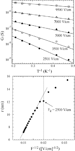
In Fig. 4(b), these values are shown as a function of . It is observed that for electric fields above , becomes proportional to , with a slope of . For lower fields, deviates from this relation and the fits become worse, probably because in this range, develops a significant temperature dependence. This observation is in qualitative agreement with the model of Dvurechenskii et al. Dvurechenskii et al. (1988), where it has been argued that in high electric fields, i.e. for , the energy gained by the electric field overcomes the activation energy such that the transport becomes activationless, which means that the last two terms in the exponent of eq. (6) cancel each other, and a temperature-independent conductivity evolves with an electric field dependence given by
| (7) |
with
| (8) |
This model predicts a slope of , in rough agreement with (i.e. 70% larger than) our value determined from the experiment. We speculate that either the dielectric constant increases in high electric fields, or the electric fields accessible in our experiment are not high enough for eq. (7) to hold, even though the same functional dependence is found. We note that similar discrepancies have been reported in the literature for other systems Yu et al. (2004).
The behavior of in large electric fields could be also attributed to Joule heating, which would be most prominent at low temperatures under high electric fields and cause a saturation of as the temperature decreases. From the heat generated at and the thermal conductivity of the oxide layer underneath the PPy film, we estimate the maximum increase of the sample temperature by Joule heating to . Therefore, the Joule heating effect can be neglected in our experiments.
Fig. 5 shows the differential conductance at as a function of for various magnetic fields, taking sample A as an example. For all electric fields, the magnetic field tends to localize the charges, thus counteracting the electric-field induced delocalization. In the inset of Fig. 5, the magnetoconductance is shown for different electric fields. For , is independent of within experimental accuracy. At , the curvature of switches from positive to negative while for larger magnetic fields, the normalized resistance change induced by becomes weaker as increases.
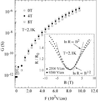
To the best of our knowledge, the magnetoresistance of a disordered medium in the variable range hopping regime under high electric fields has not been studied up to now. The theory of magnetotransport in such systems under negligible electric fields, however, is well established Shklovskii and Efros (1988); Shklovskii (1972), and in the following we use it to interpret our measurements. This seems well justified for the low magnetic field regime where only a very small influence of the electric field on is observed. According to Shklovskii and Efros Shklovskii and Efros (1988), the magnetic confinement reduces the wave function overlap between sites. Within a percolation model, this causes the resistance to increase exponentially as increases according to
| (9) |
where
| (10) |
Below , eq. 9 fits our data well, with the fit parameters and for the measurements at and , respectively. From eq. (10), we expect for sample A in good agreement with the fit parameters. For , deviations from eq. (9) are observed. Theory Shklovskii and Efros (1988); Shklovskii (1972) predicts that for negligible electric fields and ( denotes the density of impurities), the magnetoresistance has the form
| (11) |
which has been observed in several experiments Yoon et al. (1994); Kahlert et al. (1976). Our data are fitted well by eq. (11) for . The measurements indicate a value of . This would correspond to an impurity density of , i.e. an average distance between impurity sites of , much larger than the characteristic hopping distance, a result which cannot be interpreted in a straightforward way. We note that even though our data can be described qualitatively by eq. (11), its application is questionable considering the significant effect has on in this regime and the fact that is not large compared to . Also, a behavior according to eq. (11) for , i.e., outside the range of validity of eq. (11), has been observed in other experiments, see, e.g. Kahlert et al. (1976). Additional theoretical studies are required to understand this regime in more detail.
III SUMMARY AND CONCLUSIONS
The electronic transport properties of thin, chemically grown polypyrrole films have been investigated. In contrast to previous experiments performed on much thicker films, we find that Efros-Shklovskii variable range hopping dominates at temperatures below , and Arrhenius activated transport is observed at higher temperatures. Nonlinearities in the current-voltage characteristics are found, which can be interpreted within an extension of the Efros-Shklovskii model to high electric fields. In agreement with this model, we observe that the hopping distance is proportional to above a characteristic field of in our system, which marks a transition to short range hopping. Moreover, for small magnetic fields, the measured magnetoresistance is in quantitative agreement with the Shklovskii-Efros description of magnetic field induced localization in disordered media. At large magnetic fields, we observe an electric field induced reduction of the localization which requires further theoretical study.
Financial support by the Heinrich-Heine-Universität Düsseldorf is gratefully acknowledged. The authors acknowledge fruitful discussions with D. Basko.
References
- Skotheim et al. (1998) T. A. Skotheim, R. L. Elsenbaumer, and J. R. Reynolds, eds., Handbook of Conducting Polymers (Marcel Dekker, New York, 1998), 2nd ed.
- Yoon et al. (1994) C. O. Yoon, R. M., D. Moses, and A. J. Heeger, Phys. Rev. B 49, 10851 (1994).
- Asavapiriyanont et al. (1984) S. Asavapiriyanont, G. Chandler, G. Gunawardena, and D. Pletcher, J. Electroanal. Chem. 177, 229 (1984).
- Rodriguez et al. (1997) J. Rodriguez, H. J. Grande, and T. F. Cooper, Handbook of Organic Conductive Molecules and Polymers (John Wiley Sons, New York, 1997).
- Simonet and Berthelot (1991) J. Simonet and J. R. Berthelot, Prog. Solid State Chem. 21, 1 (1991).
- Yamamura et al. (1988) M. Yamamura, T. Hagiwara, and K. Iwata, Synth. Met. 26, 209 (1988).
- Kanazawa et al. (1980) K. Kanazawa, A. F. Diaz, W. D. Gill, P. M. Grant, G. B. Street, G. P. Gardini, and J. F. Kwak, Synth, Met. 1, 329 (1980).
- Diaz et al. (1981) A. Diaz, J. M. V. Vallejo, and A. M. Duran, IBM J. Res. Dev. 25, 42 (1981).
- et al. (2005) C. C. , J. Vollmer, T. Heinzel, P. Espindola, H. John, and J. Heinze, J. Phys. Chem. B 109, 19191 (2005).
- Marcos and Wolfbeis (1997) S. D. Marcos and O. S. Wolfbeis, Sens. Mater. 9, 253 (1997).
- Bidan (1992) G. Bidan, Sens. Act. B 6, 45 (1992).
- Malinauskas (2001) A. Malinauskas, Polymer 42, 3957 (2001).
- Geng et al. (2006) L. Geng, X. Huanga, Y. Zhaoa, P. Lia, S. Wanga, S. Zhanga, and S. Wu, Sol. State Elec. 50, 723 (2006).
- Cosnier (2000) S. Cosnier, Appl. Biochem. Biotechnol. 89, 127 (2000).
- Chung et al. (2005) H.-J. Chung, H. Jung, Y.-S. Cho, S. Lee, J.-H. Ha, J. Choi, and Y. Kuk, Appl. Phys. Lett. 86, 213113 (2005).
- Lee et al. (2005) M. Lee, H. Kang, H. Kang, J. Joo, A. Epstein, and J. Lee, Thin Solid Film 477, 169 (2005).
- and Heinzel (2006) C. C. and T. Heinzel, Appl. Phys. Lett. 89, 012104 (2006).
- Shklovskii and Efros (1988) B. I. Shklovskii and A. L. Efros, Electronic Properties of Doped Semiconductors (Springer-Verlag, 1988).
- Efros and Shklovskii (1975) A. L. Efros and B. I. Shklovskii, J. Phys. C 8, L49 (1975).
- Menon et al. (1998) R. Menon, C. O. Yoo, D. Moses, and A. J. Heeger, Handbook of Conducting Polymers (Marcel Dekker, New York, 1998), 2nd ed.
- Kohlman and Epstein (1998) R. S. Kohlman and A. J. Epstein, Handbook of Conducting Polymers (Marcel Dekker, New York, 1998), 2nd ed.
- Ribo et al. (1998) J. M. Ribo, M. C. Anglada, J. M. Hernandez, X. Zhang, N. Ferrer-Anglada, A. Chaibi, and B. Movaghar, Synth. Met. 97, 229 (1998).
- Gomis et al. (2003) V. Gomis, N. Ferrer-Anglada, B. Movaghar, J. M. Ribo, Z. El-Hachemi, and S. H. Jhang, Phys. Rev. B 68, 115208 (2003).
- Joo et al. (2000) J. Joo, J. K. Lee, S. Y. Lee, K. S. Jang, E. J. Oh, and A. J. Epstein, Macromolecules 33, 5131 (2000).
- Zhang et al. (2006) X. Zhang, J. Zhang, W. Song, and Z. Liu, J. Phys. Chem. B 110, 1158 (2006).
- Chakrabarti et al. (2002) S. Chakrabarti, D. Banerjee, and R. Bhattacharyya, J. Phys. Chem. 106, 3061 (2002).
- Winther-Jensen et al. (2004) B. Winther-Jensen, J. Chen, K. West, and G. Wallace, Macromolecules 37, 5930 (2004).
- Bredas et al. (1983) J. L. Bredas, B. Themans, and J. M. Andre, Phys. Rev. B 27, 7827 (1983).
- Bredas et al. (1984) J. L. Bredas, J. C. Scott, K. Yakushi, and G. B. Street, Phys. Rev. B 30, 1023 (1984).
- Van and Potje-Kamloth (2000) C. N. Van and K. Potje-Kamloth, J. Phys. D: Appl. Phys. 33, 2230 (2000).
- Koezuka and Etoh (1983) H. Koezuka and S. Etoh, J. Appl. Phys. 54, 2511 (1983).
- Mott (1974) N. F. Mott, Metal Insulator Transitions (Tayler and Francis, London, 1974).
- Tran et al. (2005) T. B. Tran, I. S. Beloborodov, X. M. Lin, T. P. Bigioni, V. M. Vinokur, and H. M. Jaeger, Phys. Rev. Lett. 95, 076806 (2005).
- Roest et al. (2003) A. Roest, J. Kelly, and D. Vanmaekelbergh, Appl. Phys. Lett. 83, 5530 (2003).
- Yu et al. (2004) D. Yu, C. Wang, B. L. Wehrenberg, and P. Guyot-Sionnest, Phys. Rev. Lett. 92, 216802 (2004).
- Dvurechenskii et al. (1988) A. V. Dvurechenskii, V. A. Dravin, and A. I. Yakimov, JETP Lett. 48, 155 (1988).
- Hill (1971) R. M. Hill, Philos. Mag. 24, 1307 (1971).
- Pollak and Riess (1976) R. M. Pollak and I. Riess, J. Phys. C 9, 2339 (1976).
- Shklovskii (1976) B. I. Shklovskii, Sov. Phys. Semicond. 10, 855 (1976).
- Shklovskii (1972) B. I. Shklovskii, Sov. Phys. Semicond. 6, 1053 (1972).
- Kahlert et al. (1976) H. Kahlert, G. Landwehr, A. Schlachetzki, and H. Salow, Z. Phys. B 276, 1 (1976).