Two path transport measurements on a triple quantum dot
Abstract
We present an advanced lateral triple quantum dot made by local anodic oxidation. Three dots are coupled in a starlike geometry with one lead attached to each dot thus allowing for multiple path transport measurements with two dots per path. In addition charge detection is implemented using a quantum point contact. Both in charge measurements as well as in transport we observe clear signatures of states from each dot. Resonances of two dots can be established allowing for serial transport via the corresponding path. Quadruple points with all three dots in resonance are prepared for different electron numbers and analyzed concerning the interplay of the simultaneously measured transport along both paths.
pacs:
73.21.La, 73.23.Hk, 73.63.KvSince observation and manipulation on the submicron scale were made possible some decades ago, a huge variety of lateral nanostructures on semiconductors has been developed and investigated to gain access to quantummechanical quantities. By now even zerodimensional quantum dots Kouwenhoven et al. (1997), so called artificial atoms, have been investigated intensively as they were proposed as crucial elements for quantum computing Loss and DiVincenzo (1998). Next to transport measurements the combination with quantum point contacts (QPC) has allowed for charge detection gaining access to new quantities like electron number or coupling symmetries e.g. Field et al. (1993); Nemutudi et al. (2004); Schleser et al. (2005); Rogge et al. (2005). For several years now double quantum dots with two dots combined to artificial molecules are subject to extensive research van der Wiel et al. (2003). Coupling phenomena and the roll of electronic spins have been studied in parallel configurations with each dot connected to both leads Holleitner et al. (2001); Rogge et al. (2003) as well as in serial systems e.g. Pioro-Ladriere et al. (2003); Elzerman et al. (2003); Petta et al. (2004); Hüttel et al. (2005).
Despite these successes and although there are interesting theoretical predictions Saraga et al. (2003); Michaelis et al. (2006); Groth et al. (2006); Emary (2006), lateral triple quantum dots have almost not been investigated so far. Some experiments were done in the early nineties Haug (2004); Waugh et al. (1995). Three experiments have been published recently with geometries based on electron beam lithography. Vidan et al. Vidan et al. (2004) investigated a serial double quantum dot with a side coupled third dot as a quantum box. Gaudreau et al. Gaudreau et al. (2006) observed charge rearrangements on a ringlike triple quantum dot in a system originally designed for double quantum dots. Schröer et al. Schröer et al. (2007) created a system with three dots in a row.
In this letter we present a different geometry for a lateral triple quantum dot. We created a starlike system with each dot placed next to the other two. In contrast to the formerly published works we have three leads connected to our system, one for each quantum dot. Thus we can simultaneously measure transport via different paths with only two dots per path.
To enable charge detection we extend our device by a QPC making the setup more flexible. With this variety of features we decided to use an atomic force microscope (AFM) to built this unique setup as this technique provides the same functionality with less gates involved compared to devices made by split gate technique with ebeam lithography. Therefore as far as we know this is the only lateral triple quantum dot made with local anodic oxidation (LAO) Ishii and Matsumoto (1995); Keyser et al. (2000).
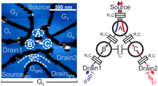
Using LAO on a GaAs/AlGaAs heterostructure oxide lines are created shown in black in the AFM-image of the device in Fig.1, left. Three dots A, B, C (see dashed circles) are defined in a starlike setup with tunnelling barriers in between. Each dot is connected to a ”personal” lead used as the source or drain contacts. Four gates G1 to G4 are used to tune the coupling to the leads and the interdot coupling. Due to the small dimensions the gates do not work independently and thus a fine balance of all four gate voltages is necessary to operate the system. For charge detection a QPC (dashed lines) is placed below dots B and C with its own source and drain leads (SourceQPC, DrainQPC) and an additional gate GQPC to tune the conductance of the QPC. The complete QPC can be used as another gate G5 for the triple dot with the charge detection still working.
The measurements were performed in a He3/He4-dilution refrigerator at a base temperature of 15 mK. AC and DC voltages were applied to one lead of the triple dot called Source while the differential conductance G through the device was measured on the other two leads called Drain1 and Drain2 individually using two lock-in setups. The QPC was operated with a DC voltage applied to SourceQPC and the DC current measured at DrainQPC. In the following the device is connected as shown in Fig. 1: the source contact is connected to dot A, Drain1 is placed at dot B and Drain2 at dot C. Thus transport can be measured in two parallel paths as shown in the schematic on the right of Fig. 1 with dots A and B in series along path 1 and dots A and C in series along path 2.
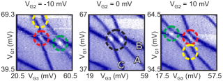
First the device is studied in the closed regime where no current is detectable along both paths. Still the charging of the device is detectable using the QPC. This is shown in Fig. 2. The derivative of the QPC current is plotted as a function of gates G3 and G1 for three different voltages at gate G2. In each measurement dark lines are visible denoting charging events in the system. As influences from the gate voltages are different for each dot the charging events show three different slopes, one for each dot. The lines with the lowest slope belong to dot B, those with the largest slope belong to dot C. The lines with intermediate slopes denote charging on dot A (see Fig. 2, V mV). Where the lines meet anticrossings are found with two dots in resonance. In Fig. 2 at V mV those anticrossings are visible for resonance between dot A and dot B (green circle, the chemical potentials for dot A and dot B are equal, with NA and NB the electron numbers on both dots), dot A and dot C (yellow circle, ) and dot B and dot C (red circle, ). Although no tunnel coupling is possible between B and C bc there is still a huge capacitive coupling demonstrating the close vicinity of the two dots. At these anticrossings bright features are visible due to charge transitions from one dot to another without changing the total charge of the system. For V mV in Fig. 2 all three anticrossings are separated by a few mV. For V mV these anticrossings coincide (black circle) thus showing the resonance condition for all three dots (). With increasing VG2 the resonances are shifted further and the three dot resonance condition is lifted again (V mV). Thus the existence of three coupled quantum dots with tunable resonance conditions is demonstrated. Furthermore, dot C can be emptied to zero electrons as the line visible for dot C is the last line detected. No further line corresponding to C appears when decreasing the gate voltages. The line visible denotes charging with the first electron ().
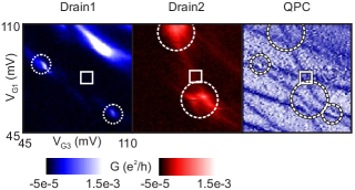
Adjusting the gate voltages and opening the barriers finite transport through the dots becomes measurable. This is shown in Fig. 3. Charge diagrams are recorded sweeping gates G3 and G1 as in Fig. 2. Next to the charge detection the differential conductance G is measured along paths 1 and 2. The measurement along path 1 is plotted in blue, the one along path 2 in red. Along both paths spot like features are visible, some of them marked with circles. Comparing these features with the QPC measurement one finds that they correspond to anticrossings of quantum dot states. The spots measured at Drain1 (small circles) correspond to resonances between dots A and B. The features measured at Drain2 (big circles) appear due to resonances between dots A and C. The latter ones are slightly split due to the strong interdot coupling of A and C. In both paths at least two spots are visible meaning that these are resonances for different electron numbers. The two marked blue spots appear for the same state on dot A but for two consecutive states on dot B. Thus at one spot dot B is charged with an even number of electrons and at the other resonance with an odd number. Similar properties account for the red features. Both spots appear for the same state on dot C, which is charging with the second electron here (transport for the first electron can be measured for different gate voltages). Two consecutive states on dot A are involved one of them with even, the other with odd electron numbers. The charge signal at the QPC shows a third group of anticrossings exemplarily marked with a square. Those correspond to resonances between dots B and C. Comparing these features with the measurements along both paths it becomes obvious that there are no corresponding features in transport. This remarkably shows the functionality of the two path setup with a common source contact and two drain contacts. In each path the two dots placed there must be in resonance to allow for serial transport. Resonances of two dots in different paths are not sufficient to generate finite differential conductance.
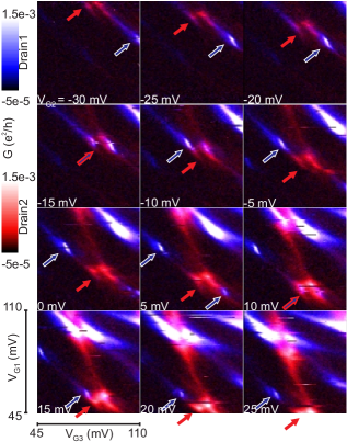
With the ability of measuring conductance along two paths simultaneously but separately our device enables a novel way of data analysis by plotting the data in advanced color scale plots. This is demonstrated in 12 consequent plots in Fig. 4, that show both signals simultaneously in one plot but separated by different colors (red for path 1, blue for path 2). Thus this way of plotting suits perfectly the original data recording. Features in both paths can be compared immediately and assigned to the appropriate path. For example the strong blue to white features in the upper part of the last three plots are split into two. One can directly see that this comes from a red feature that splits the blue features due to interdot coupling.
The main aspect of the 12 consequent plots in Fig. 4 is to study the way triple resonances appear in transport. Similar as in Fig. 2 the resonances visible in transport can be shifted to establish resonances of all three quantum dots. For each measurement shown in Fig. 4 VG2 is set to a fixed voltage starting from -30 mV at the upper left and increased to 25 mV at the lower right. Both paths show spot like features due to resonance of two dots (color encoded as in Fig. 3) some of them marked with blue and red arrows. While the red spots move downwards with increasing VG2 the blue spots move to the left. Thus using gate G2 resonance conditions of all three dots can be created. The two spots marked with a red and a blue arrow for V mV (chemical potentials and ) for example approach each other with increasing VG2. At V mV both spots have merged, simultaneous transport via path 1 and path 2 is detected, the three dots are in resonance (). Thereby the blue resonance is split into two resonances due to the strong anticrossing for the red spot (a similar splitting of the red spot is almost not observable due to the much weaker anticrossing for the blue spot). A further increase of VG2 moves the blue and red spots apart again. The same happens with the red spot and another blue spot coming into resonance at V mV (). The two triple resonances differ by one electron on dot B. As mentioned before further resonances are visible at higher VG1 ( at V mV). Here the electron number on dot A has changed as well. Similar results were gained stepping VG4 instead of VG2.
Thus not only with charge detection, even in transport we can detect clear resonances of two quantum dots in two different paths in combined color plots. Shifting these resonances quadruple points can be formed with all three dots in resonance. These quadruple points can be prepared for different electron numbers creating odd or even configurations on each dot and thus on the whole triple dot as well. Therefore this device is promising to verify theoretical predictions published recently for two path triple quantum dots. A two path triple dot can be used as a spin entangler Saraga et al. (2003) with a spin singlet formed in dot A for an even number of electrons. As mentioned before we can prepare an even number of electrons for each dot. The entangled spins are then separated and transferred to the two drain leads with one electron per path thus creating spin entangled currents. Refs. Michaelis et al. (2006); Groth et al. (2006); Emary (2006) predict the formation of a trapped state for electrons entering the triple dot via dots B and C. A coherent superposition of charge in the two dots can be created with destructive interference at dot A blocking transport. Depending on the needed direction of the current flow through the two paths one could use different setups of source and drain contacts on our device to establish the appropriate conditions for both experiments.
In conclusion we have investigated resonances of two and three quantum dots in transport and with charge detection in a lateral triple dot device made with local anodic oxidation. The three dots are arranged in a starlike geometry with each of them coupled to the other two. Three leads, one for each dot, allow for simultaneous transport measurements via different paths. States from all three dots were detected in charge measurements showing anticrossings when two dots come into resonance. Adjusting the four gate voltages it was possible to establish resonances for all three dots. This tunability was confirmed in transport measurements at different gate voltages. Via two paths transport was measured simultaneously with each path showing resonances of two dots. Resonance conditions were established with simultaneous transport via both paths with all three dots in resonance. The formation of these quadruple points was analyzed for both paths simultaneously in combined color scale plots for different electron numbers.
This work has been supported by BMBF via nanoQUIT.
References
- Kouwenhoven et al. (1997) L. P. Kouwenhoven, C. M. Marcus, P. L. McEuen, S. Tarucha, R. M. Westervelt, and N. S. Wingreen, in Mesoscopic Electron Transport, edited by L. L. Sohn, L. P. Kouwenhoven, and G. Schön (Kluwer, Dordrecht, 1997), vol. 345 of Series E, pp. 105–214.
- Loss and DiVincenzo (1998) D. Loss and D. P. DiVincenzo, Phys. Rev. A 57, 120 (1998).
- Field et al. (1993) M. Field, C. G. Smith, M. Pepper, D. A. Ritchie, J. E. F. Frost, G. A. C. Jones, and D. G. Hasko, Phys. Rev. Lett. 70, 1311 (1993).
- Nemutudi et al. (2004) R. Nemutudi, M. Kataoka, C. J. B. Ford, N. J. Appleyard, M. Pepper, D. A. Ritchie, and G. A. C. Jones, J. Appl. Phys. 95, 2557 (2004).
- Schleser et al. (2005) R. Schleser, E. Ruh, T. Ihn, K. Ensslin, D. C. Driscoll, and A. C. Gossard, Phys. Rev. B 72, 035312 (2005).
- Rogge et al. (2005) M. C. Rogge, B. Harke, C. Fricke, F. Hohls, M. Reinwald, W. Wegscheider, and R. J. Haug, Phys. Rev. B 72, 233402 (2005).
- van der Wiel et al. (2003) W. G. van der Wiel, S. D. Franceschi, J. M. Elzerman, T. Fujisawa, S. Tarucha, and L. P. Kouwenhoven, Rev. Mod. Phys. 75, 1 (2003).
- Holleitner et al. (2001) A. W. Holleitner, C. R. Decker, H. Qin, K. Eberl, and R. H. Blick, Phys. Rev. Lett. 87, 256802 (2001).
- Rogge et al. (2003) M. C. Rogge, C. Fühner, U. F. Keyser, R. J. Haug, M. Bichler, G. Abstreiter, and W. Wegscheider, Appl. Phys. Lett. 83, 1163 (2003).
- Pioro-Ladriere et al. (2003) M. Pioro-Ladriere, M. Ciorga, J. Lapointe, P. Zawadzki, M. Korkusinski, P. Hawrylak, and A. S. Sachrajda, Phys. Rev. Lett. 91, 026803 (2003).
- Elzerman et al. (2003) J. M. Elzerman, R. Hanson, J. S. Greidanus, L. H. Willems van Beveren, S. De Franceschi, L. M. K. Vandersypen, S. Tarucha, and L. P. Kouwenhoven, Phys. Rev. B 67, 161308(R) (2003).
- Petta et al. (2004) J. R. Petta, A. C. Johnson, C. M. Marcus, M. P. Hanson, and A. C. Gossard, Phys. Rev. Lett. 93, 186802 (2004).
- Hüttel et al. (2005) A. K. Hüttel, S. Ludwig, H. Lorenz, K. Eberl, and J. P. Kotthaus, Phys. Rev. B 72, 081310(R) (2005).
- Saraga et al. (2003) D. S. Saraga, and D. Loss, Phys. Rev. Lett. 90, 166803 (2003).
- Michaelis et al. (2006) B. Michaelis, C. Emary, and C. W. J. Beenakker, Europhys. Lett. 73, 677 (2006).
- Groth et al. (2006) C. W. Groth, B. Michaelis, and C. W. J. Beenakker, Phys. Rev. B 74, 125315 (2006).
- Emary (2006) C. Emary, cond-mat/07052934.
- Haug (2004) R. J. Haug, Electrochimica Acta 40, 1283 (1995).
- Waugh et al. (1995) F. R. Waugh, M. J. Berry, D. J. Mar, R. M. Westervelt, K. L. Campman, and A. C. Gossard, Phys. Rev. Lett. 75, 705 (1995).
- Vidan et al. (2004) A. Vidan, R. M. Westervelt, M. Stopa, M. Hanson, and A. C. Gossard, Appl. Phys. Lett. 85, 3602 (2004).
- Gaudreau et al. (2006) L. Gaudreau, S. A. Studenikin, A. S. Sachrajda, P. Zawadzki, A. Kam, J. Lapointe, M. Korkusinski, and P. Hawrylak, Phys. Rev. Lett. 97, 036807 (2006).
- Schröer et al. (2007) D. Schröer, A. D. Greentree, L. Gaudreau, K. Eberl, L. C. L. Hollenberg, J. P. Kotthaus, and S. Ludwig, cond-mat/0703450.
- (23) With Source at dot B and Drain at A and C we found, that the barrier connecting dots B and C cannot be opened while keeping the dots working even with 210 mV applied to gate G5. The low tunability originates from the fact that there is only one large gate (G5) on that side of the device.
- Ishii and Matsumoto (1995) M. Ishii and K. Matsumoto, Jpn. J. Appl. Phys. 34, 1329 (1995).
- Keyser et al. (2000) U. F. Keyser, H. W. Schumacher, U. Zeitler, R. J. Haug, and K. Eberl, Appl. Phys. Lett. 76, 457 (2000).