Ultrathin oxides: bulk-oxide-like model surfaces or unique films?
Abstract
To better understand the electronic and chemical properties of wide-gap oxide surfaces at the atomic scale, experimental work has focused on epitaxial films on metal substrates. Recent findings show that these films are considerably thinner than previously thought. This raises doubts about the transferability of the results to surface properties of thicker films and bulk crystals. By means of density-functional theory and approximate corrections for the electronic spectra we demonstrate for three characteristic wide-gap oxides (silica, alumina, and hafnia) the influence of the substrate and highlight critical differences between the ultrathin films and surfaces of bulk materials. Our results imply that monolayer-thin oxide films have rather unique properties.
pacs:
68.47.Gh; 73.20.-r; 71.20.Ps;On the nanoscale materials often reveal new and unexpected features. In particular ultrathin oxide films have recently generated increasing interest. First, thin oxide films themselves play an important role in technological applications such as electronic devices, fuel cells, gas sensors, corrosion and scratch protection, or heterogeneous catalysts. Second, they are increasingly used as model oxides in the surface science approach to thicker or bulk-like oxides: Many experimental techniques such as scanning tunneling microscopy or photoemission spectroscopy cannot be directly applied to insulating materials, but require electrically conducting samples. Ultrathin epitaxial oxide films on metal substrates overcome this limitation Goodman (2003); Freund (2002); Schroeder et al. (2000, 2002); Chen et al. (2004); Weissenrieder et al. (2005); Giordano et al. (2005); Chen and Goodman (2006); Wendt et al. (2005); Jaeger et al. (1991); Kresse et al. (2005); Kulawik et al. (2006). However, the direct transfer of experimental conclusions from these films to bulk oxide surfaces relies on the two critical assumptions that a) the thickness dependence of the film and b) substrate-film interactions are negligible for the surface properties (cf. Fig. 1). In the present letter we argue that the finite thickness and the presence of the substrate modify the film’s geometry and/or stoichiometry in a way that is unknown and maybe even impossible for surfaces of thicker films and bulk crystals. In addition, the coupling of the film to the metal’s Fermi level may induce charge transfer Giordano et al. (2003). The resulting mechanical, electronic, and chemical properties may then differ considerably from the systems that were the original goal of the study. Instead, these ultrathin films should be considered as new materials with interesting and novel properties of their own.
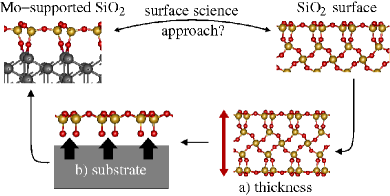
For a meaningful comparison between thin films and bulk oxides one has to first identify the oxide surfaces with the closest resemblance to the ultrathin film. Then, one would like to isolate the influence of the substrate from that of the finite thickness or the thickness dependence in the surface science approach, to analyze each contribution separately. While the latter is not possible with the experimental tools available to date, it is easily achieved in theory by the hypothetical two-step pathway shown in Fig. 1: a) reduce the thickness of free-standing films and study the effect of the thickness variation b) place an ultrathin film on a substrate analyzing the substrate dependence. In this Letter, we employ density-functional theory (DFT) in the local-density approximation (LDA) rem (a) to address these questions for three representative thin-film oxide systems: 1) silica on Mo(112), a recent prototypical surface science model for ceramic support materials of heterogeneous catalysts, 2) alumina, which in various modifications is also frequently applied as model substrate for catalytic reactions, and 3) hafnia, the material of choice in the most advanced microprocessor technology ITR .
For silica, flat and well-ordered films have successfully been grown on Mo(112) by Freund et al. and by Goodman et al. Schroeder et al. (2000, 2002); Chen et al. (2004). Recent ab initio simulations Weissenrieder et al. (2005); Giordano et al. (2005) suggest a two-dimensional network structure (isostructural, as we will show below, to the -quartz (0001) surface Rignanese et al. (2000)), whereas Goodman et al. favor an isolated [SiO4] cluster model Chen and Goodman (2006). Indications for thickness effects were given by Wendt et al., who have demonstrated in a comparative study including thicker (but amorphous) films that the electronic structure varies with the film thickness Wendt et al. (2005). Alumina films have been grown on a wide variety of substrates, e.g., Re, Mo, Ni3Al, NiAl, or Fe3Al. A typical, intensively studied example is NiAl(110), where a well-ordered alumina film of defined thickness is obtained by a direct oxidation of the alloy’s surface Jaeger et al. (1991). Its complex structure is governed by the interplay between the local, preferentially hexagonal ordering of the oxide and its linkage to the Al atoms at the interface to the metal alloy Kresse et al. (2005). Recent STM experiments for the adsorption of small gold cluster on this film have shown that surface properties are modified by the film’s substrate Kulawik et al. (2006). Ultrathin hafnia films on metallic substrates have not been investigated so far.
To investigate how far ultrathin films could reflect the surface properties of macroscopic samples in principle we first exclude the substrate influence by studying free-standing silica, alumina, and hafnia films. For all three oxides we find substantial differences between monolayer (ML)-thin and thicker films. We concentrate on the atomic structure and the electronic density of states (DOS). Many other properties are correlated to these two key aspects, e.g., the atomic configuration and the local electronic structure determine the chemical activity. The films are fully relaxed within the surface unit cell of the most stable bulk surface, i.e., the (0001) surfaces of -quartz (silica) Rignanese et al. (2000) and -alumina Wang et al. (2000), and the (111) surface of cubic hafnia rem (b). This ensures that, upon increasing the thickness, the films systematically develop towards the bulk limit.
For silica, we have compared a variety of surface terminations and reconstructions. We find that the most stable films are stoichiometric and have fully saturated bonds. The structures represent perfect networks of [SiO4] units, in agreement with the trends in bulk silicates Liebau (1985). This similarity in the local geometry is contrasted by the flexibility of the bonding network that easily adjusts to the constraints imposed by the finite thickness and leads to quite different structures for each thickness. Films with more than 4 formula units are best described as -quartz-like layers sandwiched between two reconstructed surfaces with three-membered silica rings at the interface Rignanese et al. (2000) (Si5O10 being highly distorted). In the Si4O8 film, which has no intermediate layers, the reconstructed surfaces are directly linked together. Si2O4 consists of a single-layer network with two-membered silica rings, a motif known from other silica surfaces Giordano et al. (2005); Ceresoli et al. (2000).
The structural variations in the alumina and hafnia films are less drastic, but significant for ultrathin films, too. For example, the outermost Al atom of the alumina surface is known to strongly relax inward Wang et al. (2000). This relaxation shows a pronounced thickness dependence. The interlayer spacing is reduced by 62% for the Al4O6 film, by 96% for Al6O9, and 87% for Al8O12 and thicker films. The relaxations at the hafnia surface are smaller (4% of the interlayer spacing), but the thinnest films again deviate from their thicker counterparts. The trend towards smaller structural changes reflects the higher coordination in alumina (6/4 for Al/O, respectively) and hafnia (8/4 for Hf/O) compared to silica (4/2 for Si/O) which limits the geometrical flexibility.
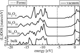
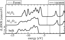
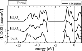
The effect of the finite thickness on the electronic and chemical properties can be analyzed in terms of the DOS, displayed for selected films in Fig. 2. While the wide-gap insulating character of the perfect films is not affected by the thickness, the peak structure of the DOS differs significantly for ultrathin films. Since defect levels are most likely subject to the same shifts as the bands from which they derive, this implies that ML-thin films may show critical deviations in their defect properties. Fig. 2 highlights the differences in the local DOS at the surface (the detailed evolution of the electronic structure will be discussed elsewhere) comparing the surface DOS of one or two ultrathin films to a thick film, more representative for macroscopic samples, and the total DOS of the bulk. In all three cases, the ultrathin films have a unique peak structure that differs from that of thicker films. These varying peaks are not associated with particular local orbitals but must be considered properties of the overall electronic structure. In addition, the Al4O6 film shows a remarkable reduction of the band gap, while the valence band width is comparable to that of thicker films and also the bulk. This indicates an overall weakening of the Madelung potential when a substantial amount of the ions is undercoordinated Giordano et al. (2003). In all other cases, the band widths and gaps are close to their bulk values. In general, we find that the changes in the electronic structure follow those in the local atomic structure, which underlines the crucial importance of the latter.
Of course, supported films are additionally influenced by the interface to their substrate. Yet, our results for free-standing films clearly demonstrate that the ML-thin films cannot be considered representative for the structural, electronic, defect, or surface properties of the respective bulk materials in contrast to earlier statements Goodman (2003); Freund (2002); Schroeder et al. (2000); Jaeger et al. (1991). Only when the films are thicker than 3-4 layers, the surface properties of defect-free surfaces are approaching those of bulk-like systems. This is a noticeable smaller film thickness than known for metal surfaces, where for closed packed surfaces typically around 8 in some cases even up to 20 layers Chis and Hellsing (2004) are needed, but in line with other ionic materials such as NaCl Li et al. (2006). We attribute this trend to the degree of localization of the valence electrons in these materials, which is larger in the insulators (considered here) than in metals with typical semiconductors in between. The deviating behavior of ML-thin films offers the prospect that experimentally accessible ultrathin oxide films such as silica on Mo(112) may be understood as new and unique materials in their own right, opening possible new routes to devise insulator surfaces with novel properties.
We will now in more detail discuss the role of the substrate for the example of silica on Mo(112), assuming the recently suggested structure model Weissenrieder et al. (2005); Giordano et al. (2005) (denoted as “siloxane surface”): Corner-sharing [SiO4] tetrahedrons form a two-dimensional, perfectly bonded hexagonal network, that is linked to the Mo surface via oxygen (cf. Fig. 1). The film has a Si2O5 stoichiometry that does not naturally occur in bulk silica. A comparison to other known thin film and surface structures reveals that it is identical to the “dense reconstruction” of the -quartz (0001) surface Rignanese et al. (2000), the “silicate adlayer” on 4H and 6H SiC Bernhardt et al. (1999), and the “siloxane surface” of clay minerals Sposito (1984). The correspondence to the -quartz surface (which apparently has not been recognized previously) makes the silica film on Mo(112) an ideal candidate for studying the role of the metal substrate. For this, we regard the -quartz layers below the siloxane surface as an alternative, insulating substrate in place of Mo(112).
Focusing on the structural aspects first, we find that the siloxane surface adapts to the substrate by reorienting the [SiO4] tetrahedrons as rigid units, a behavior well-known for silicates Liebau (1985). A substrate-independent, “ideal” siloxane surface structure was determined from a free-standing siloxane double layer (Si4O8). Its optimized lattice constant (5.24 Å) is very close to the quasihexagonal c() Mo(112) superlattice (a=5.21 Å and =63∘) and also to the ()R30∘ pattern (5.25 Å) observed for SiC Bernhardt et al. (1999), whereas the lattice mismatch to -quartz (4.85 Å) amounts to 8%. This provides a simple explanation why the siloxane surface forms readily on the lattice-matched substrates Mo(112) and 4H/6H-SiC (0001), while it has not been possible to prepare it experimentally on -quartz. A further important factor is the linkage of the silica film to the Mo rows on Mo(112). The threefold symmetry axis of the [SiO4] tetrahedrons is tilted by 14∘ against the surface normal (cf. Fig. 1). This introduces a height difference (buckling) for the surface atoms of 0.4 Å. The siloxane surface on quartz, however, tilts only by 4∘ and buckles by 0.2 Å. We conclude that the siloxane surface on Mo(112), used in the surface science experiments, exhibits new features and deviates noticeable from the ideal -quartz surface despite the identical chemical connectivity.
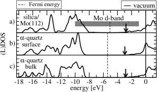
To visualize the substrate’s influence on the electronic structure, the local DOS for the siloxane surface on Mo(112) and -quartz are presented in Fig. 3 along with the total DOS of bulk -quartz as a reference. The band edges at the surface agree with those of -quartz to within 0.5 eV for both substrates. There are no surface states in the large band gap. The Mo metal states, which energetically lie within the surface band gap, play no important role at the surface. However, the peak structure in the valence region of the surface DOS differs for the two substrates and deviates also from the DOS of bulk -quartz. We have analyzed the origin of these changes by placing the silica/Mo surface structure on quartz and find that mainly the structural variations are responsible for the changes observed, whereas the chemically different interface plays a minor role.
| UPSa | –11.5 | –10.6 | – | –7.6 | – | –6.3 | –5.6c |
|---|---|---|---|---|---|---|---|
| MIESa | –11.6c | –10.4 | – | –7.6 | –6.7 | – | – |
| DFT-LDAb | –9.5 | –8.3 | –7.3 | –5.6 | –4.9 | –4.3 | –3.8c |
a From Fig. 4c) in Wendt et al. Wendt et al. (2005); b this work; c shoulder
That the surface electronic structure of the well-ordered silica film on Mo(112) possesses a unique peak structure has been observed in ultraviolet photoelectron spectroscopy (UPS) and metastable impact electron spectroscopy (MIES) Schroeder et al. (2002); Wendt et al. (2005). For comparing the DFT-LDA DOS to experimental spectra, we focus on the peak positions since the spectral intensities depend on the spectroscopic method and even make some peaks disappear in the experimental MIE and UP spectra Wendt et al. (2005). To overcome limitations of DFT-KS in describing the quasiparticle spectrum probed in experiment, we employ many-body perturbation theory in the approximation Aul ; Rinke et al. (2005). In , the electronic self-energy (which connects the non-interacting electrons of DFT-KS to the truly interacting ones) is given by the product of the Green function and the screened interaction . is typically applied as a correction scheme to the DFT-LDA energies which corrects deficiencies of the LDA and includes quasiparticle effects Aul ; Rinke et al. (2005). We have performed calculations for bulk -quartz. Transferring in a first crude approximation the bulk corrections to the silica film, we estimate that the silica features in the valence region are shifted downward by 2 eV. Taking this correction into account, the agreement with experiment (cf. Tab. 1) becomes very good. This agreement not only supports the siloxane surface as structural model for the silica film on Mo(112), but also shows that the peaks observed in experiment are not generic silica features, but specific to the actual film.
In light of these results we argue that the silica film on Mo(112) must in fact be considered a novel oxidic surface, as envisioned from free-standing films, and is not simply another incarnation of a siloxane surface on bulk -quartz. The lattice mismatch of 8% to -quartz (which may prevent the formation of large ordered domains in real samples) induces important changes in the structure compared to Mo(112), which subsequently modifies the electronic structure.
In summary we find that ultrathin films of wide-gap oxides require two or three bulk-like layers to develop the characteristic properties of the bulk materials and their surfaces. This implies that ML-films are no simple analog of thicker films or realistic oxide surfaces. In addition, we demonstrated significant substrate-induced changes in the surface structure and electronic properties for the experimentally accessible silica film on Mo(112). We expect that similar conclusions hold for other metal-supported oxide films. Thus, ML-epitaxial thin films should not be seen merely as models for thick oxides in heterogeneous catalysis or other applications. Instead they may offer a unique way to devise entirely “new” insulator surfaces in surface science or catalysis.
References
- Goodman (2003) D. Goodman, J. Catal. 216, 213 (2003).
- Freund (2002) H.-J. Freund, Surf. Sci. 500, 271 (2002).
- Schroeder et al. (2000) T. Schroeder, M. Adelt, B. Richter, M. Naschitzki, M. Bäumer, and H.-J. Freund, Surf. Rev. Lett. 7, 7 (2000).
- Schroeder et al. (2002) T. Schroeder, J. B. Giorgi, M. Bäumer, and H.-J. Freund, Phys. Rev. B 66, 165422 (2002).
- Chen et al. (2004) M. S. Chen, A. K. Santra, and D. W. Goodman, Phys. Rev. B 69, 155404 (2004).
- Weissenrieder et al. (2005) J. Weissenrieder, S. Kaya, J.-L. Lu, H.-J. Gao, S. Shaikhutdinov, H.-J. Freund, M. Sierka, T. K. Todorova, and J. Sauer, Phys. Rev. Lett. 95, 076103 (2005).
- Giordano et al. (2005) L. Giordano, D. Ricci, G. Pacchioni, and P. Ugliengo, Surf. Sci. 584, 225 (2005).
- Chen and Goodman (2006) M. Chen and D. W. Goodman, Surf. Sci. Lett. 600, L255 (2006).
- Wendt et al. (2005) S. Wendt, E. Ozensoy, T. Wei, M. Frerichs, Y. Cai, M. S. Chen, and D. W. Goodman, Phys. Rev. B 72, 115409 (2005).
- Jaeger et al. (1991) R. M. Jaeger, H. Kuhlenbeck, H.-J. Freund, M. Wuttig, W. Hoffmann, R. Franchy, and H. Ibach, Surf. Sci. 259, 235 (1991).
- Kresse et al. (2005) G. Kresse, M. Schmid, E. Napetschnig, M. Shishkin, L. Köhler, and P. Varga, Science 308, 1440 (2005).
- Kulawik et al. (2006) M. Kulawik, N. Nilius, and H.-J. Freund, Phys. Rev. Lett. 96, 036103 (2006).
- Giordano et al. (2003) L. Giordano, J. Goniakowski, and G. Pacchioni, Phys. Rev. B 67, 045410 (2003).
- rem (a) We employ a plane-wave basis and norm-conserving pseudopotentials. The surfaces and thin films are modeled in the repeated-slab approach.
- (15) The latest International Technology Roadmap for Semiconductors is available online at http://www.itrs.net/.
- Rignanese et al. (2000) G.-M. Rignanese, A. De Vita, J.-C. Charlier, X. Gonze, and R. Car, Phys. Rev. B 61, 13250 (2000).
- Wang et al. (2000) X.-G. Wang, A. Chaka, and M. Scheffler, Phys. Rev. Lett. 84, 3650 (2000).
- rem (b) We have chosen the cubic modification rather than the thermodynamically stable monoclinic one, because it appears to play an important role in hafnia thin films Aarik et al. (2001); Van Elshocht et al. (2004).
- Liebau (1985) F. Liebau, Structural Chemistry of Silicates (Springer, Berlin Heidelberg, 1985).
- Ceresoli et al. (2000) D. Ceresoli, M. Bernasconi, S. Iarlori, M. Parrinello, and E. Tosatti, Phys. Rev. Lett. 84, 3887 (2000).
- Chis and Hellsing (2004) V. Chis and B. Hellsing, Phys. Rev. Lett. 93, 226103 (2004).
- Li et al. (2006) B. Li, A. Michaelides, and M. Scheffler, Phys. Rev. Lett. 97, 046802 (2006).
- Bernhardt et al. (1999) J. Bernhardt, J. Schardt, U. Starke, and K. Heinz, Appl. Phys. Lett. 74, 1084 (1999).
- Sposito (1984) G. Sposito, The surface chemistry of soils (Oxford Univ. Press, 1984).
- (25) W. G. Aulbur, L. Jönsson, and J. W. Wilkins in Solid State Physics, edited by H. Ehrenreich and F. Spaepen (Academic, New York, 2000), vol. 54, p 1.
- Rinke et al. (2005) P. Rinke, A. Qteish, J. Neugebauer, C. Freysoldt, and M. Scheffler, New J. Phys. 7, 126 (2005).
- Aarik et al. (2001) J. Aarik, A. Aidla, H. Mändar, T. Uustare, K. Kukli, and M. Schuisky, Appl. Surf. Sci 173, 15 (2001).
- Van Elshocht et al. (2004) S. Van Elshocht et al., J. Electrochem. Soc. 151, F228 (2004).