Light quasiparticles dominate electronic transport in molecular crystal field-effect transistors
Abstract
We report on an infrared spectroscopy study of mobile holes in the accumulation layer of organic field-effect transistors based on rubrene single crystals. Our data indicate that both transport and infrared properties of these transistors at room temperature are governed by light quasiparticles in molecular orbital bands with the effective masses m⋆ comparable to free electron mass. Furthermore, the m⋆ values inferred from our experiments are in agreement with those determined from band structure calculations. These findings reveal no evidence for prominent polaronic effects, which is at variance with the common beliefs of polaron formation in molecular solids.
A comprehensive understanding of charge transport in organic semiconductors poses a significant intellectual challenge and, at the same time, is crucial for further advances in the field of “plastic electronics”Malliaras ; Forrest . One longstanding problem pertains to the nature of the electronic excitations responsible for charge transport in these systemsCapek ; GershRMP . A commonly used descriptionCapek is that the electrical current in these easily polarizable materials is carried by polarons: electrons or holes strongly coupled to local lattice deformations. A hallmark of the polaronic transport is a strong enhancement of the effective mass compared to the band valuesCapek . Therefore, the hypothesis of polaron formation in molecular crystals is verifiable since the effective masses of mobile charges can be directly probed in infrared (IR) spectroscopic measurements.
Here we report on IR spectroscopy studies of charge carriers in the conducting channel of organic field-effect transistors (OFET) based on single crystals of rubrene (C42H28, Fig.1b inset), a small-molecule organic semiconductorGershRMP ; GerRev04 ; VPprl04 ; VPprl05 . These studies show that charge transport in rubrene based OFETs at room temperature is dominated by light quasiparticles in the highest occupied molecular orbital(HOMO) band. New spectroscopy data along with band structure calculations help to elucidate recent observations of non-activated, diffusive charge transport at the surface of high-quality molecular crystals in studies of single-crystal OFETsGershRMP ; GerRev04 ; VPprl04 ; VPprl05 .

A schematic of the rubrene OFETs studied here is displayed in the inset of Fig. 1a. In these devices, source and drain graphite or silver paint contacts were prepared on the surface of a rubrene single crystal followed by the deposition of approximately 1 of parylene that serves as the gate insulatorGerRev04 . The gate-channel capacitance per unit area in this type of devices is 2.1 nF/cm2. For gate electrode, we used a 24-nm-thick layer of InSnOx (ITO) with the electron density cm-3 and the sheet resistance 300 /square, deposited by dc-magnetron sputtering in pure argon. The gate electrode covers the entire device area (up to ). We studied the IR response of numerous OFETs with typical DC transport mobility 5 cm2V-1s-1 at room temperature. The use of the semitransparent electrode ITO enabled spectroscopic studies of the field-induced accumulation layer (AL) in rubrene from far-IR up to 2.2 eV, the band gap of rubrene. In our IR measurements, free-standing rubrene OFETs were illuminated with linearly polarized light over the frequency range 30 - 18000 cm-1 (4 meV-2.2 eV) with a spectral resolution of 4 cm-1 using a home-built set-up for broad band micro-spectroscopy. We investigated the IR transmission of the OFETs, T(,VGS), as a function of frequency and the voltage applied between the gate and source electrodes, VGSDressel . The source and drain electrodes were held at the same potential in most measurements.
We first examine the transmission spectra T() of a bare rubrene single crystal (Fig.1b), which are instructive for the understanding of the response of rubrene OFETs. The sharp absorption lines below 5000 cm-1 originate from phonons. The abrupt suppression of T() at about 18000 cm-1 is due to the lowest interband transition between HOMO and LUMO (lowest unoccupied molecular orbital) bands. The interband transitions, the phonon frequencies and the overall transmission level are all anisotropic within the -plane.
Fig.1a depicts the T(,VGS)/T(,VGS=0V) spectra for a representative OFET at 300K, obtained with the E vector along the axis and axis. Similar results were found in all devices we investigated. Under an applied gate voltage, a pronounced suppression of the transmission of the transistor is observed, which is stronger for the polarization of the E vector along the -axis of the rubrene crystal. The effect is most prominent at far-IR frequencies and peaked near 400 cm-1. The form of T(VGS)/T(0V) traces does not change appreciably with the applied voltage, whereas the magnitude varies nearly linearly with VGS. These observations suggest that the changes of IR properties of our devices are intimately related to the formation of ALs both in the channel of the OFET and in the ITO gate electrode. Using IR microscopyLiNanoLett we have verified that the density of induced carriers is uniform along the channel of the OFETs. Therefore, the two dimensional (2D) carrier density in our OFETs can be estimated as follows:
| (1) |
where is the elementary charge.
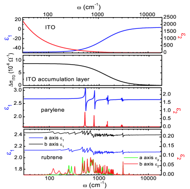
In order to characterize the dynamical properties of the charges in the field-induced AL at the rubrene-parylene interface, it is imperative to extract the optical constants of this layer. We employed an analysis protocol that takes into account all the layers in our devices: 1) ITO, 2) AL at the ITO-parylene interface characterized by the 2D conductivity , 3) parylene, 4) AL at the rubrene-parylene interface with the 2D conductivity and 5) bulk rubrene crystal. The response of layers 1, 3 and 5 was assumed to be voltage independent, whereas layers 2 and 4 reveal voltage-dependent properties. We first evaluated the complex dielectric function ()=()+i()=1+4i()/ for layers 1, 3 and 5 from a combination of reflection, transmission and ellipsometric measurements performed on layers with the same thicknesses as the ones used in the OFETs, as shown in Fig. 2. We then extracted from the Drude model: , where the relaxation rate =1300 cm-1 and effective mass =0.5 were determined from the measurements of ITO films, and carrier density of ITO AL was obtained from Eq.(1). Finally, we employed a multi-oscillator fitting procedureKuzmenko to account for the contribution of to the transmission of the device calculated from standard methods for multi-layered structures. The spectra extracted using this routine are shown in Fig. 3 whereas the T(VGS=-280V)/T(0V) spectra generated from the multilayer model are plotted in Fig.1a. Alternatively the response of our devices can be described by Eq.(3) in Ref.Tsui , which directly relates the raw T(VGS)/T(0V) data to the 2D conductivity of the ALs. The spectra inferred from these two methods are in agreement within an accuracy of 10 %, which is comparable to the error in the raw data. Fig.1a depicts the contribution of to the raw T(VGS)/T(0V) data obtained by omitting the rubrene AL from the model, which shows that voltage-induced changes of the electron density in ITO result in a measurable change in the transmission. Note that the contribution of ITO to the T(VGS)/T(0V) spectra has a monotonic frequency dependence in contrast to the non-monotonic form of the overall transmission change of the device.
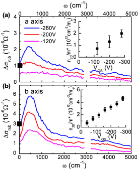
Fig. 3 displays the optical conductivity spectra of the 2D system of field-induced quasiparticles at the rubrene-parylene interface for the polarization of the E vector along the and axes. Similar to the raw T(VGS)/T(0V) data, the conductivity spectra are characterized by a finite energy peak centered at around 400 cm-1. At lower frequencies, decreases toward the DC value that was obtained independently in DC transport measurements. In the near-IR range, is negligibly small as shown in Fig.1a. In particular, no noticeable features were observed in at frequencies close to the band gap of rubrene. The anisotropy of the conductivity spectra is found throughout the IR range and extends to the DC limit. Importantly, remains finite with the temperature decreasing down to 30 K (not shown) in the entire IR range down to at least 80-90 cm-1. We therefore conclude that no sizable energy gap opens up in the IR response of the AL formed by voltage-induced holes in rubrene.
The non-monotonic form of the conductivity spectra in Fig. 3 can be qualitatively described by the localization-modified Drude model that is commonly used to account for the IR properties of organic materials and other disordered conductors in the vicinity of metal-insulator transitionsMottKaveh . This description is not unique. We therefore will focus on the overall strength of the spectra, which allows us to evaluate the optical effective mass of the field-induced quasiparticles using the model-independent oscillator strength sum ruleWooten ,
| (2) |
The cutoff frequency is chosen to be 5000 cm-1 to accommodate the entire energy region where voltage-induced changes are prominent. increases linearly with VGS for both and data (insets in Fig. 3), which is consistent with the capacitive model Eq.(1) provided that does not change within the range of applied biases. This agreement further justifies the use of Eq.(1) for extracting the charge density in the AL, which approaches cm-2 at -280 V. The slopes of (VGS) for the and measurements are different as shown in Fig. 3. This result in conjunction with Eqs. (1), (2) yields the anisotropy of the effective mass: and . The direct spectroscopic observation of the mass anisotropy elucidates the origin of the anisotropic electronic mobility observed in transport measurementsGershRMP ; GerRev04 ; VPprl04 ; VPprl05 . Indeed the magnitude of the anisotropy of is in good agreement with that of the mobility within experimental errors; this suggests that the anisotropic effective masses of mobile quasiparticles dominate the directional dependence of transport properties.
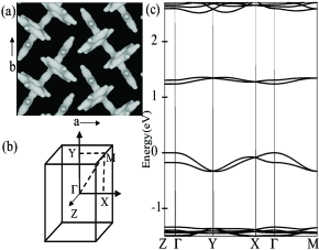
To understand the experimental data, we have carried out first-principles density functional theory (DFT) calculations of the band structure of rubrene within the generalized gradient approximation (GGA)Becke using the experimental lattice parametersKafer , as displayed in Fig. 4. The orthorhombic unit cell has two planes separated by half a unit cell in the direction, each containing two inequivalent rubrene molecules. We find however that the interactions between the planes in the unit cell are negligible. From fitting the top of the HOMO band with parabolic functions over different energy ranges along the -X and -Y directions, we obtained effective masses in the range of values 1.92.8 and 1.01.3 for hole carriers along the a and b directions, respectively. The DFT-GGA functional may also contribute to errors in the computed band masses. Nevertheless, the band mass values are overall comparable to those of the field-induced quasiparticles inferred from IR measurements. The difference between the two could be due to the errors in these quantities as discussed above. Therefore, our IR study, along with band structure calculations, reveals no significant enhancement of the effective mass of the quasiparticles in rubrene OFETs compared to the band values.
Our IR studies of charge dynamics in rubrene OFETs and band structure calculations unveil several unexpected aspects of the quasiparticles in these systems. First, no low-energy gap in the optical conductivity is observed in the whole IR range suggesting that the field-induced quasiparticles reside in a continuum of electronic states extending both above and below the Fermi energy. The states involved in quasiparticle dynamics reflect the intrinsic electronic structure of rubrene with rather distinct values of overlap integrals in the - and -directions. This conclusion is attested by the anisotropy of transport properties, IR conductivity and most importantly by the effective masses directly determined from IR data. Rather light effective masses of mobile quasiparticles once again point to the involvement of band states (within the HOMO band) in the electronic response in agreement with the band structure analysis. These findings suggest that the periodic potential of the molecular crystal lattice and the electronic band structure play a dominant role in charge dynamics even at room temperature. Because organic molecular crystals are periodic systems, the concept of energy bands in these systems at sufficiently low temperatures is not in dispute. However, in view of the weak inter-molecular van-der-Waals bonds in these crystals, the long-range order may be disrupted by the thermally-induced dynamic disorderTroisi . Nevertheless, our results show that the band dispersion evaluated in the limit of T0 provides an accurate account of transport and IR properties at room temperature. The notion of light quasiparticles in the HOMO band established through these findings is furthermore supported by recent observations of non-activated, diffusive charge transport on the surface of high-quality molecular crystalsGershRMP ; GerRev04 ; VPprl04 ; VPprl05 , also suggesting the existence of extended electronic states.
Light effective masses comparable to band values reported here have not been foreseen by theoretical models commonly postulating very strong coupling between electronic and lattice degrees of freedom in molecular solids leading to the formation of small polarons even at room temperature. Small polarons are characterized by large masses of at least several times the band mass due to the coupling with latticeCapek in stark contrast with our observations. Therefore, our work indicates that polaronic effects in rubrene OFETs are weaker at room temperature than previously thought, and the charge transport can be adequately described by quasiparticles in the HOMO band. This assertion is furthermore supported by the frequency dependence of the optical conductivity. Polarons in organic systems (including OFETs) typically give rise to broad resonances in the absorption spectra in mid-IR frequenciesLiNanoLett that are not detected in our data for rubrene-based transistors. We conclude that the polaron binding energies in rubrene must be below 26 meV, the energy that corresponds to room temperature. Future work will be aimed at establishing if polaronic effects in general, and enhancement of the effective mass in particular, may be responsible for a rapid suppression of the conductivity below 140 KVPprl04 .
Work at UCSD is supported by the NSF, DOE and PRF. Work at Rutgers University is supported by the NSF grants DMR-0405208 and ECS-0437932. The Advanced Light Source is supported by the Director, Office of Science, Office of Basic Energy Sciences, of the U.S. Department of Energy under Contract No. DE-AC02-05CH11231.
References
- (1) G. Malliaras and R.H. Friend, Phys. Today 58, 53 (2005).
- (2) S.R. Forrest, Nature 428, 911 (2004).
- (3) E.A. Silinsh and V. Capek, Organic Molecular Crystals: Interaction, Localization, and Transport Phenomena (AIP Press, New York, 1994).
- (4) M.E. Gershenson, V. Podzorov, and A.F. Morpurgo, Rev. Mod. Phys. 78, 973 (2006); C.H. Ahn et al., Rev. Mod. Phys. 78, 1185 (2006).
- (5) R.W.I. de Boer, M.E. Gershenson, A.F. Morpurgo, and V. Podzorov, Phys. Status Solidi A 201, 1302 (2004).
- (6) V. Podzorov et al., Phys. Rev. Lett. 93, 086602 (2004).
- (7) V. Podzorov, E. Menard, J. A. Rogers, and M. E. Gershenson, Phys. Rev. Lett. 95, 226601 (2005).
- (8) IR properties of rubrene OFETs were also studied in another recent work: M. Fischer et al., Appl. Phys. Lett. 89, 182103 (2006).
- (9) Z. Q. Li et al., Nano Lett. 6 , 224 (2006).
- (10) A. B. Kuzmenko, Rev. Sci. Instrum. 76, 083108 (2005); N. Sai et al., Phys. Rev. B 75, 045307 (2007).
- (11) D.C. Tsui et al., Surface Science 73, 419 (1978).
- (12) N.F. Mott and M. Kaveh, Adv. Phys. 34, 329 (1985).
- (13) F. Wooten, Optical Properties of Solids (Academic, New York/London, 1972).
- (14) A.D. Becke, Phys. Rev. A 38, 3098 (1988); C. Lee, W. Yang, and R.G. Parr, Phys. Rev. B 37, 785 (1988). We used the package for the calculations. (http://dft.sandia.gov/Socorro/mainpage.html). Common density functionals such as the GGA used in this work do not account for van der Waals forces, which determine the correct distance between molecules. However, when the bonding distances are fixed at the experimental ones, this deficiency has negligible effect on the electronic dispersion that is mainly determined by the overlap of the electronic wave functions.
- (15) D. Kafer and G. Witte, Phys. Chem. Chem. Phys. 7, 2850 (2005); E. Menard et al., Adv. Mater. 18, 1552 (2006).
- (16) A. Troisi and G. Orlandi, Phys. Rev. Lett. 96, 086601 (2006).